research
In the digitized modern life, various forms of future displays, such as wearable and rollable displays are required. More and more people are wanting to connect to the virtual world whenever and wherever with the use of their smartglasses or smartwatches. Even further, we’ve been hearing about medical diagnosis kit on a shirt and a theatre-hat. However, it is not quite here in our hands yet due to technical limitations of being unable to fit as many pixels as a limited surface area of a glasses while keeping the power consumption at the a level that a hand held battery can supply, all the while the resolution of 4K+ is needed in order to perfectly immerse the users into the augmented or virtual reality through a wireless smartglasses or whatever the device.
KAIST (President Kwang Hyung Lee) announced on the 22nd that Professor Sang Hyeon Kim's research team of the Department of Electrical and Electronic Engineering re-examined the phenomenon of efficiency degradation of micro-LEDs with pixels in a size of micrometers (μm, one millionth of a meter) and found that it was possible to fundamentally resolve the problem by the use of epitaxial structure engineering.
Epitaxy refers to the process of stacking gallium nitride crystals that are used as a light emitting body on top of an ultrapure silicon or sapphire substrate used for μLEDs as a medium.
μLED is being actively studied because it has the advantages of superior brightness, contrast ratio, and lifespan compared to OLED. In 2018, Samsung Electronics commercialized a product equipped with μLED called 'The Wall'. And there is a prospect that Apple may be launching a μLED-mounted product in 2025.
In order to manufacture μLEDs, pixels are formed by cutting the epitaxial structure grown on a wafer into a cylinder or cuboid shape through an etching process, and this etching process is accompanied by a plasma-based process. However, these plasmas generate defects on the side of the pixel during the pixel formation process.
Therefore, as the pixel size becomes smaller and the resolution increases, the ratio of the surface area to the volume of the pixel increases, and defects on the side of the device that occur during processing further reduce the device efficiency of the μLED. Accordingly, a considerable amount of research has been conducted on mitigating or removing sidewall defects, but this method has a limit to the degree of improvement as it must be done at the post-processing stage after the grown of the epitaxial structure is finished.
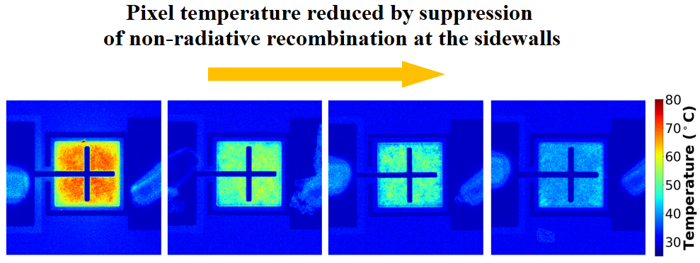
The research team identified that there is a difference in the current moving to the sidewall of the μLED depending on the epitaxial structure during μLED device operation, and based on the findings, the team built a structure that is not sensitive to sidewall defects to solve the problem of reduced efficiency due to miniaturization of μLED devices. In addition, the proposed structure reduced the self-generated heat while the device was running by about 40% compared to the existing structure, which is also of great significance in commercialization of ultrahigh-resolution μLED displays.
This study, which was led by Woo Jin Baek of Professor Sang Hyeon Kim's research team at the KAIST School of Electrical and Electronic Engineering as the first author with guidance by Professor Sang Hyeon Kim and Professor Dae-Myeong Geum of the Chungbuk National University (who was with the team as a postdoctoral researcher at the time) as corresponding authors, was published in the international journal, 'Nature Communications' on March 17th. (Title of the paper: Ultra-low-current driven InGaN blue micro light-emitting diodes for electrically efficient and self-heating relaxed microdisplay).
Professor Sang Hyeon Kim said, "This technological development has great meaning in identifying the cause of the drop in efficiency, which was an obstacle to miniaturization of μLED, and solving it with the design of the epitaxial structure.“ He added, ”We are looking forward to it being used in manufacturing of ultrahigh-resolution displays in the future."
This research was carried out with the support of the Samsung Future Technology Incubation Center.

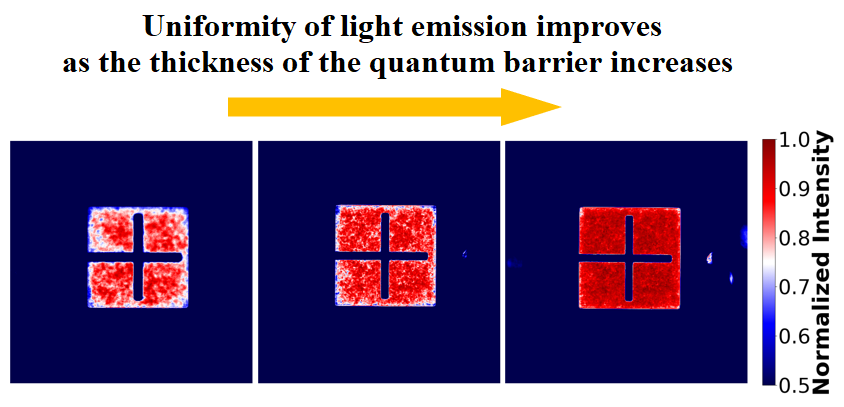
Figure 1. Image of electroluminescence distribution of μLEDs fabricated from epitaxial structures with quantum barriers of different thicknesses while the current is running

Figure 2. Thermal distribution images of devices fabricated with different epitaxial structures under the same amount of light.

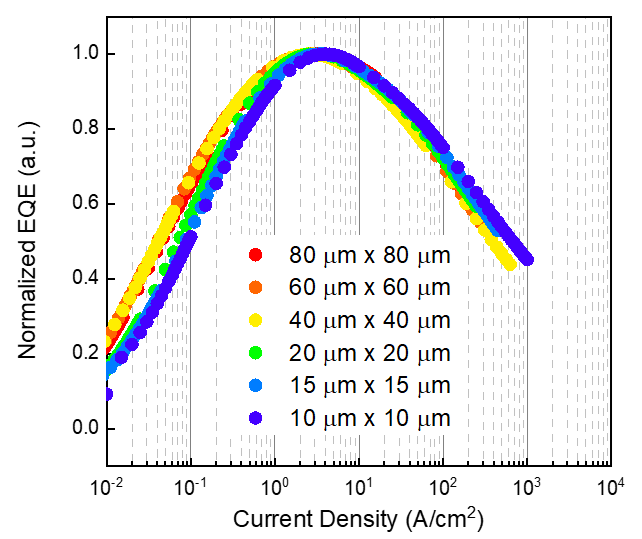
Figure 3. Normalized external quantum efficiency of the device fabricated with the optimized epitaxial structure by sizes.
-
research A KAIST Team Develops Face-Conforming LED Mask Showing 340% Improved Efficacy in Deep Skin Elasticity
- A KAIST research team led by Professor Keon Jae Lee has developed a deep skin-stimulating LED mask which has been verified in clinical trials to improve dermis elasticity by 340%. < Figure 1. Overall concept of face-fit surface-lighting micro-LEDs (FSLED) mask. a. Optical image of the FSLED mask showing uniform surface-lighting. schematic illustration of the FSLED mask. The 2D to 3D transformation procedure b. Difference in cosmetic effect on deep skin elasticity, wrinkles, and sagging
2024-10-29 -
research KAIST finds ways for Bacteria to produce PET-like materials
Among various eco-friendly polymers, polyhydroxyalkanoates (PHA) stand out for their excellent biodegradability and biocompatibility. They decompose naturally in soil and marine environments and are used in applications such as food packaging and medical products. However, natural PHA produced to date has faced challenges meeting various physical property requirements, such as durability and thermal stability, and has been limited in its commercial application due to low production concentration
2024-08-28 -
research KAIST Develops Microbial Liquid Egg Substitute
A team of researchers published a paper on developing a substitute for eggs using microorganisms, grabbing international attention. It is expected that the development of egg substitutes using non-animal raw materials will solve the problems of factory farming, which causes problems like increased emission of greenhouse gas and waste, and contribute to building a sustainable food system that allows easy protein intake. KAIST (President Kwang-Hyung Lee) announced that Research Professor Kyeong R
2024-07-05 -
research Novel High-performance and Sustainable Paper Coating Material created by KAIST-Yonsei University Research Team to reduce microplastic pollution
What if there is a biodegradable packaging material with high performance without leaving microplastics? Plastic pollution presents a global challenge that must be solved. In particular, packaging accounts for 30-50% of the total plastic consumption. While paper packaging is eco-friendly, it lacks crucial functionalities like moisture resistance and strength. Traditional coating materials exacerbate plastic pollution, prompting the need for sustainable alternatives. Polyethylene (PE) and e
2024-05-22 -
research KAIST introduces microbial food as a strategy food production of the future
The global food crisis is increasing due to rapid population growth and declining food productivity to climate change. Moreover, today's food production and supply system emit a huge amount of carbon dioxide, reaching 30% of the total amount emitted by humanity, aggravating climate change. Sustainable and nutritious microbial food is attracting attention as a key to overcoming this impasse. KAIST (President Kwang Hyung Lee) announced on April 12th that Research Professor Kyeong Rok Choi of th
2024-04-12