research

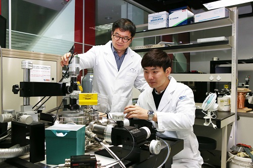
(Professor Choi and Ph.D. candidate Jang)
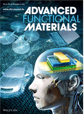
KAIST research team led by Professor Sung-Yool Choi at School of Electrical Engineering and Professor Sung Gap Im at the Department of Chemical and Biomolecular Engineering developed high-density, ultra-low power, non-volatile, flexible memory technology using 2D materials. The team used ultrathin molybdenum disulfide (MoS2) with atomic-scale thickness as the channel material and high-performance polymeric insulator film as the tunneling dielectric material. This research was published on the cover of Advanced Functional Materials on November 17. KAIST graduate Myung Hun Woo, a researcher at Samsung Electronics and Ph.D. candidate Byung Chul Jang are first authors.
The surge of new technologies such as Internet of Things (IoT), Artificial Intelligence (AI), and cloud server led to the paradigm shift from processor-centric computing to memory-centric computing in the industry, as well as the increase in demand of wearable devices. This led to an increased need for high-density, ultra-low power, non-volatile flexible memory. In particular, ultrathin MoS2 as semiconductor material has been recently regarded as post-silicon material. This is due to its ultrathin thickness of atomic-scale which suppresses short channel effect observed in conventional silicon material, leading to advantages in high- density and low-power consumption. Further, this thickness allows the material to be flexible, and thus the material is applicable to wearable devices.
However, due to the dangling-bond free surface of MoS2 semiconductor material, it is difficult to deposit the thin insulator film to be uniform and stable over a large area via the conventional atomic layer deposition process. Further, the currently used solution process makes it difficult to deposit uniformly low dielectric constant (k) polymeric insulator film with sub-10 nm thickness on a large area, thus indicating that the memory device utilizing the conventional solution-processed polymer insulator film cannot be operated at low-operating voltage and is not compatible with photolithography.
The research team tried to overcome the hurdles and develop high-density, ultra-low power, non-volatile flexible memory by employing a low-temperature, solvent-free, and all-dry vapor phase technique named initiated chemical vapor deposition (iCVD) process. Using iCVD process, tunneling polymeric insulator film with 10 nm thickness was deposited uniformly on MoS2 semiconductor material without being restricted by the dangling bond-free surface of MoS2. The team observed that the newly developed MoS2-based non-volatile memory can be operated at low-voltage (around 10V), in contrast to the conventional MoS2-based non-volatile memory that requires over 20V.
Professor Choi said, “As the basis for the Fourth Industrial revolution technologies including AI and IoT, semiconductor device technology needs to have characteristics of low-power and flexibility, in clear contrast to conventional memory devices.” He continued, “This new technology is significant in developing source technology in terms of materials, processes, and devices to contribute to achieve these characteristics.”
This research was supported by the Global Frontier Center for Advanced Soft Electronics and the Creative Materials Discovery Program by funded the National Research Foundation of Korea of Ministry of Science and ICT.

( Figure 1. Cover of Advanced Functional Materials)

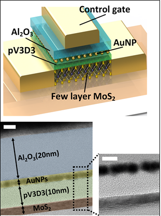
(Figure 2. Concept map for the developed non-volatile memory material and high-resolution transmission electron microscopy image for material cross-section )
-
research New Catalyst Recycles Greenhouse Gases into Fuel and Hydrogen Gas
< Professor Cafer T. Yavuz (left), PhD Candidate Youngdong Song (center), and Researcher Sreerangappa Ramesh (right) > Scientists have taken a major step toward a circular carbon economy by developing a long-lasting, economical catalyst that recycles greenhouse gases into ingredients that can be used in fuel, hydrogen gas, and other chemicals. The results could be revolutionary in the effort to reverse global warming, according to the researchers. The study was published on February 1
2020-02-17 -
research Novel Material Properties of Hybrid Perovskite Nanostructures for Next-generation Non-linear Electronic Devices
(from left: Juho Lee, Dr. Muhammad Ejaz Khan and Professor Yong-Hoon Kim) A KAIST research team reported a novel non-linear device with the founding property coming from perovskite nanowires. They showed that hybrid perovskite-derived, inorganic-framework nanowires can acquire semi-metallicity, and proposed negative differential resistance (NDR) devices with excellent NDR characteristics that resulted from a novel quantum-hybridization NDR mechanism, implying the potential of perovskite nano
2019-02-22 -
research Hierarchical Porous Titanium Nitride Synthesized by Multiscale Phase Separation for LSBs
(from left: Professor Jinwoo Lee and PhD candidate Won-Gwang Lim) A KAIST research team developed ultra-stable, high-rate lithium-sulfur batteries (LSBs) by using hierarchical porous titanium nitride as a sulfur host, and achieved superior cycle stability and high rate performance for LSBs. The control of large amounts of energy is required for use in an electric vehicle or smart grid system. In this sense, the development of next-generation secondary batteries is in high
2019-01-28 -
research Highly Scalable Process to Obtain Stable 2D Nanosheet Dispersion
(Professor Do Hyun Kim and his team) A KAIST team developed technology that allows the mass production of two-dimensional (2D) nanomaterial dispersion by utilizing the characteristic shearing force of hydraulic power. The 2D nanosheet dispersion can be directly applied to solution-based processes to manufacture devices for electronics as well as energy storage and conversion. It is expected to be used in these devices with improved performance. There have been numero
2018-12-19 -
research Characteristics of Submesoscale Geophysical Turbulence Reported
A KAIST research team has reported some of unique characteristics and driving forces behind submesoscale geophysical turbulence. Using big data analysis on ocean surface currents and chlorophyll concentrations observed using coastal radars and satellites has brought better understanding of oceanic processes in space and time scales of O(1) kilometer and O(1) hour. The outcomes of this work will lead to improved tracking of water-borne materials and performance in global and regional climate
2018-12-13