research

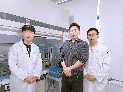
< from left: MS cadidate Jeong-Chan Lee, Professor Steve Park and PhD candidate Jin-Oh Kim >
A KAIST research team led by Professor Steve Park from the Department of Materials Science and Engineering
To overcome this issue, the research team developed an inorganic polymer micropillar-based solution shearing system to increase the crystal size of an organic semiconductor with pillar size. Using this technique, the crystallization process of organic semiconductors can be controlled precisely, and therefore large-area organic semiconductor thin film with controlled crystallinity can be fabricated.
A variety of solution-based coating techniques cannot control the fluid-flow of solutions appropriately, so the solvent evaporates randomly onto the substrate, which has difficulty in the fabrication of organic semiconductor thin film with a large crystal size.
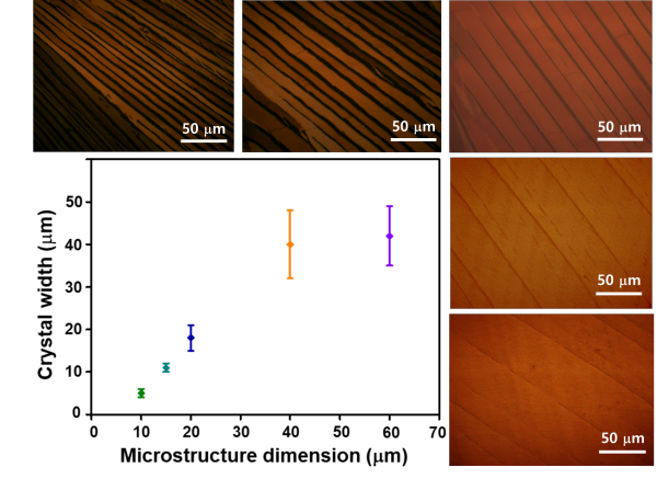
The research team integrated inorganic polymer microstructures into the solution shearing blade to solve this issue. The inorganic polymer can easily be microstructured via conventional molding techniques, has high mechanical durability, and organic solvent resistance. Using the inorganic polymer-based microstructure blade, the research team controlled the size of small molecule organic semiconductors by tuning the shape and dimensions of the microstructure. The microstructures in the blade induce the sharp curvature regions in the meniscus line that formed between the shearing blade and the substrate, and therefore nucleation and crystal growth can be regulated. Hence, the research team fabricated organic semiconductor thin-film with large crystals, which increases the field-effect mobility.
The research team also demonstrated a solution shearing process on a curved surface by using a flexible inorganic polymer-based shearing blade, which expands the applicability of solution shearing.
Professor Park said, “Our new solution shearing system can control the crystallization process precisely during solvent evaporation.” He added, “This technique adds another key parameter that can be utilized to tune the property of thin films and opens up a wide variety of new applications.
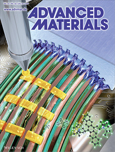
The results of this work entitled “Inorganic Polymer Micropillar-Based Solution Shearing of Large-Area Organic Semiconductor Thin Films with Pillar-Size-Dependent Crystal Size” was published in the July 2018 issue of Advanced Materials as a cover article.

< Figure 1. Cover article of the July 2018 Issue of Advanced Materials >

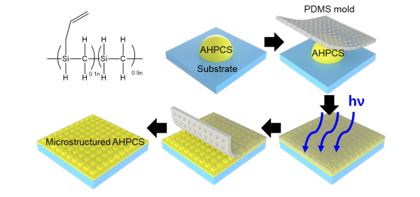
< Figure 2. Chemical structure of inorganic polymer (AHPCS) and the fabrication process of a microstructured AHPCS shearing blade. >

< Figure 3.The increasing trend of organic semiconductor crystal size with increasing the microstructure dimension. >
-
research Novel Material Properties of Hybrid Perovskite Nanostructures for Next-generation Non-linear Electronic Devices
(from left: Juho Lee, Dr. Muhammad Ejaz Khan and Professor Yong-Hoon Kim) A KAIST research team reported a novel non-linear device with the founding property coming from perovskite nanowires. They showed that hybrid perovskite-derived, inorganic-framework nanowires can acquire semi-metallicity, and proposed negative differential resistance (NDR) devices with excellent NDR characteristics that resulted from a novel quantum-hybridization NDR mechanism, implying the potential of perovskite nano
2019-02-22 -
research Hierarchical Porous Titanium Nitride Synthesized by Multiscale Phase Separation for LSBs
(from left: Professor Jinwoo Lee and PhD candidate Won-Gwang Lim) A KAIST research team developed ultra-stable, high-rate lithium-sulfur batteries (LSBs) by using hierarchical porous titanium nitride as a sulfur host, and achieved superior cycle stability and high rate performance for LSBs. The control of large amounts of energy is required for use in an electric vehicle or smart grid system. In this sense, the development of next-generation secondary batteries is in high
2019-01-28 -
research Highly Scalable Process to Obtain Stable 2D Nanosheet Dispersion
(Professor Do Hyun Kim and his team) A KAIST team developed technology that allows the mass production of two-dimensional (2D) nanomaterial dispersion by utilizing the characteristic shearing force of hydraulic power. The 2D nanosheet dispersion can be directly applied to solution-based processes to manufacture devices for electronics as well as energy storage and conversion. It is expected to be used in these devices with improved performance. There have been numero
2018-12-19 -
research Characteristics of Submesoscale Geophysical Turbulence Reported
A KAIST research team has reported some of unique characteristics and driving forces behind submesoscale geophysical turbulence. Using big data analysis on ocean surface currents and chlorophyll concentrations observed using coastal radars and satellites has brought better understanding of oceanic processes in space and time scales of O(1) kilometer and O(1) hour. The outcomes of this work will lead to improved tracking of water-borne materials and performance in global and regional climate
2018-12-13 -
research Silk Adhesive Paves the Way for Epidermal Electronics
(from left: Dr. Ji-Won Seo, Professor Hyunjoo Jenny Lee and PhD candidate, Hyojung Kim) Producing effective epidermal electronics requires a strong, biocompatible interface between a biological surface and a sensor. Here, a KAIST team employed a calcium-modified silk fibroin as a biocompatible and strong adhesive. This technology led to the development of epidermal electronics with strong adhesion for patients who need drug injections and physiological monitoring over a long
2018-11-21