research
Professor Sung-Yool Choi’s research team from KAIST's Department of Electrical Engineering has developed a technique that can produce a single-layer graphene from a metal etching. Through this, transferring a graphene layer onto a circuit board can be done as easily as stamping a seal on paper.
The research findings were published in the January 14th issue of Small as the lead article.
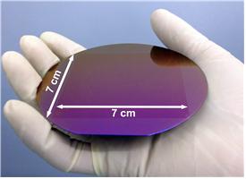
This technology will allow different types of wafer transfer methods such as transfer onto a surface of a device or a curved surface, and large surface transfer onto a 4 inch wafer. It will be applied in the field of wearable smart gadgets through commercialization of graphene electronic devices.
The traditional method used to transfer graphene onto a circuit board is a wet transfer. However, it has some drawbacks as the graphene layer can be damaged or contaminated during the transfer process from residue from the metal etching. This may affect the electrical properties of the transferred graphene.
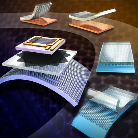
After a graphene growth substrate formed on a catalytic metal substrate is pretreated in an aqueous poly vinyl alcohol (PVA) solution, a PVA film forms on the pretreated substrate. The substrate and the graphene layers bond strongly. The graphene is lifted from the growth substrate by means of an elastomeric stamp.
The delaminated graphene layer is isolated state from the elastomeric stamp and thus can be freely transferred onto a circuit board. As the catalytic metal substrate can be reused and does not contain harmful chemical substances, such transfer method is very eco-friendly.
Professor Choi said, “As the new graphene transfer method has a wide range of applications and allows a large surface transfer, it will contribute to the commercialization of graphene electronic devices.” He added that “because this technique has a high degree of freedom in transfer process, it has a variety of usages for graphene and 2 dimensional nano-devices.”
This research was sponsored by the Ministry of Science, ICT and Future Planning, the Republic of Korea.
Figure 1. Cover photo of the journal Small which illustrates the research findings

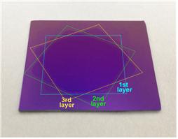
Figure 2. Above view of Graphene layer transferred through the new method

Figure 3. Large surface transfer of Graphene

-
research Highly Uniform and Low Hysteresis Pressure Sensor to Increase Practical Applicability
< Professor Steve Park (left) and the First Author Mr. Jinwon Oh (right) > Researchers have designed a flexible pressure sensor that is expected to have a much wider applicability. A KAIST research team fabricated a piezoresistive pressure sensor of high uniformity with low hysteresis by chemically grafting a conductive polymer onto a porous elastomer template. The team discovered that the uniformity of pore size and shape is directly related to the uniformity of the sensor. The
2019-08-19 -
research Novel Material Properties of Hybrid Perovskite Nanostructures for Next-generation Non-linear Electronic Devices
(from left: Juho Lee, Dr. Muhammad Ejaz Khan and Professor Yong-Hoon Kim) A KAIST research team reported a novel non-linear device with the founding property coming from perovskite nanowires. They showed that hybrid perovskite-derived, inorganic-framework nanowires can acquire semi-metallicity, and proposed negative differential resistance (NDR) devices with excellent NDR characteristics that resulted from a novel quantum-hybridization NDR mechanism, implying the potential of perovskite nano
2019-02-22 -
research Hierarchical Porous Titanium Nitride Synthesized by Multiscale Phase Separation for LSBs
(from left: Professor Jinwoo Lee and PhD candidate Won-Gwang Lim) A KAIST research team developed ultra-stable, high-rate lithium-sulfur batteries (LSBs) by using hierarchical porous titanium nitride as a sulfur host, and achieved superior cycle stability and high rate performance for LSBs. The control of large amounts of energy is required for use in an electric vehicle or smart grid system. In this sense, the development of next-generation secondary batteries is in high
2019-01-28 -
research Highly Scalable Process to Obtain Stable 2D Nanosheet Dispersion
(Professor Do Hyun Kim and his team) A KAIST team developed technology that allows the mass production of two-dimensional (2D) nanomaterial dispersion by utilizing the characteristic shearing force of hydraulic power. The 2D nanosheet dispersion can be directly applied to solution-based processes to manufacture devices for electronics as well as energy storage and conversion. It is expected to be used in these devices with improved performance. There have been numero
2018-12-19 -
research Characteristics of Submesoscale Geophysical Turbulence Reported
A KAIST research team has reported some of unique characteristics and driving forces behind submesoscale geophysical turbulence. Using big data analysis on ocean surface currents and chlorophyll concentrations observed using coastal radars and satellites has brought better understanding of oceanic processes in space and time scales of O(1) kilometer and O(1) hour. The outcomes of this work will lead to improved tracking of water-borne materials and performance in global and regional climate
2018-12-13