semiconductor+device
-
 Neuromorphic Memory Device Simulates Neurons and Synapses
Simultaneous emulation of neuronal and synaptic properties promotes the development of brain-like artificial intelligence
Researchers have reported a nano-sized neuromorphic memory device that emulates neurons and synapses simultaneously in a unit cell, another step toward completing the goal of neuromorphic computing designed to rigorously mimic the human brain with semiconductor devices.
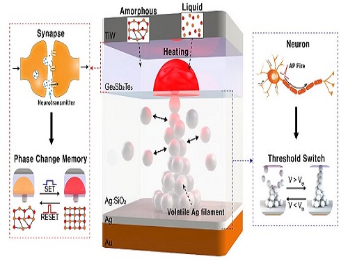
Neuromorphic computing aims to realize artificial intelligence (AI) by mimicking the mechanisms of neurons and synapses that make up the human brain. Inspired by the cognitive functions of the human brain that current computers cannot provide, neuromorphic devices have been widely investigated. However, current Complementary Metal-Oxide Semiconductor (CMOS)-based neuromorphic circuits simply connect artificial neurons and synapses without synergistic interactions, and the concomitant implementation of neurons and synapses still remains a challenge. To address these issues, a research team led by Professor Keon Jae Lee from the Department of Materials Science and Engineering implemented the biological working mechanisms of humans by introducing the neuron-synapse interactions in a single memory cell, rather than the conventional approach of electrically connecting artificial neuronal and synaptic devices.
Similar to commercial graphics cards, the artificial synaptic devices previously studied often used to accelerate parallel computations, which shows clear differences from the operational mechanisms of the human brain. The research team implemented the synergistic interactions between neurons and synapses in the neuromorphic memory device, emulating the mechanisms of the biological neural network. In addition, the developed neuromorphic device can replace complex CMOS neuron circuits with a single device, providing high scalability and cost efficiency.
The human brain consists of a complex network of 100 billion neurons and 100 trillion synapses. The functions and structures of neurons and synapses can flexibly change according to the external stimuli, adapting to the surrounding environment. The research team developed a neuromorphic device in which short-term and long-term memories coexist using volatile and non-volatile memory devices that mimic the characteristics of neurons and synapses, respectively. A threshold switch device is used as volatile memory and phase-change memory is used as a non-volatile device. Two thin-film devices are integrated without intermediate electrodes, implementing the functional adaptability of neurons and synapses in the neuromorphic memory.
Professor Keon Jae Lee explained, "Neurons and synapses interact with each other to establish cognitive functions such as memory and learning, so simulating both is an essential element for brain-inspired artificial intelligence. The developed neuromorphic memory device also mimics the retraining effect that allows quick learning of the forgotten information by implementing a positive feedback effect between neurons and synapses.”
This result entitled “Simultaneous emulation of synaptic and intrinsic plasticity using a memristive synapse” was published in the May 19, 2022 issue of Nature Communications.
-Publication:Sang Hyun Sung, Tae Jin Kim, Hyera Shin, Tae Hong Im, and Keon Jae Lee (2022) “Simultaneous emulation of synaptic and intrinsic plasticity using a memristive synapse,” Nature Communications May 19, 2022 (DOI: 10.1038/s41467-022-30432-2)
-Profile:Professor Keon Jae Leehttp://fand.kaist.ac.kr
Department of Materials Science and EngineeringKAIST
2022.05.20 View 9806
 -
 Professor Tae-Eog Lee Receives December's Scientist of the Month Award by the Korean Government
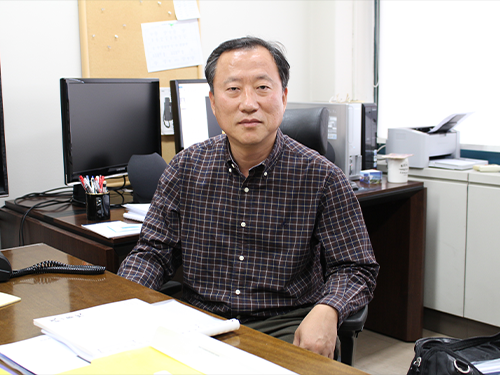
Professor Tae-Eog Lee of the Industrial and Systems Engineering at KAIST received the Scientist of the Month Award for December 2015. The award is sponsored by the Ministry of Science, ICT and Future Planning of Korea, which was hosted by the National Research Foundation of Korea.
The award recognizes Professor Lee’s efforts to advance the field of semiconductor device fabrication processing. This includes the development of the most efficient scheduling and controlling of cluster tools. He also created mathematical solutions to optimize the complicated cycle time of cluster tools in semiconductor manufacturing and the process of robot task workload.
Professor Lee contributed to the formation of various discrete event systems and automation systems based on his mathematical theories and solutions and advanced a scheduling technology for the automation of semiconductor production.
He has published 18 research papers in the past three years and has pioneered to develop Korean tool schedulers through the private sector-university cooperation.
2015.12.10 View 6343
 -
 KAIST Develops Core Technology to Synthesize a Helical Nanostructure
Professor Dong-Ki Yoon’s research team of the Graduate School of Nanoscience and Technology (GSNT) at KAIST has developed helical nanostructures using self-assembly processes. The results were published in the Proceedings of the National Academy of Sciences of the United States of America(PNAS) on the October 7th.
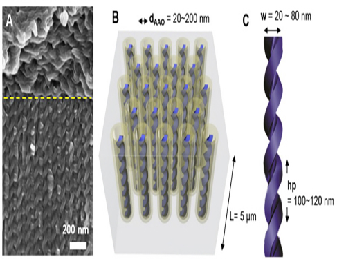
This technology enables the synthesis of various helical structures on a relatively large confined area. Its synthesis is often considered the most arduous for three dimensional structures. Formed from liquid crystal, the structure holds a regular helical structure within the confined space of 20 to 300 nanometers. Also, the distance between each pattern increased as the diameter of the nanostructure increased.
Liquid crystals have a unique property of responding sensitively to the surrounding electromagnetic field. The technology, in combination with the electromagnetic property of liquid crystal, is expected to foster the development of highly efficient optoelectronic devices.
Using this technology, it is possible to develop three dimensional patterning technology beyond the current semiconductor manufacturing technology which uses two dimensional photolithography processes. Three-dimensional semiconductor devices are expected to store hundred times more data than current devices. They will also lower costs by simplifying manufacturing processes.
The essence of this research, “self-assembly in confined space,” refers to controlling complex nanostructures, which can be synthesized from materials such as macromolecules, liquid crystal molecules, and biomolecules in relation to surrounding environments including the temperature, concentration, and pH.
The research team produced a confined space with a length of tens of nanometers by using a porous anodized aluminum membrane induced from an electrochemical reaction. They successfully synthesized independently controlled helical nanostructures by forming the helical structures from liquid crystal molecules within that space.
Professor Yoon said, “This research examines the physicochemical principle of controlling helical nanostructures.” He highlighted the significance of the research and commented, “The technology enables the control of complex nanostructures from organic molecules by using confined space and surface reforming.”
He added that, “When grafted with nanotechnology or information technology, this technology will spur new growth to liquid crystal-related industries such as the LCD.”
The research was led by two Ph.D. candidates, Hanim Kim and Sunhee Lee, under the guidance of Professor Yoon. Dr. Tae-Joo Shin of the Pohang Accelerator Laboratory, Professor Sang-Bok Lee of the University of Maryland, and Professor Noel Clark of the University of Colorado also participated.
Picture 1. Electron Microscopy Pictures and Conceptual Diagrams of Helical Nanostructures
Picture 2. Electron Microscopy Pictures of Manufactured Helical Nanostructures
2014.10.29 View 8261