research
Professors Myung-Ki Kim and Yong-Hee Lee, both of the Physics Department at KAIST, and their research teams have developed a three dimensional (3D) gap-plasmon antenna which can focus light into a space a few nanometers wide. Their research findings were published in the June 10th issue of Nano Letters.
Focusing light into a point-like space is an active research field with many applications. However, concentrating light into a smaller space than its wavelength is often hindered by diffraction. To tackle this problem, many researchers have utilized the plasmonic phenomenon of a metal where light can be confined to a greater extent by overcoming the diffraction limit.
Many researchers have focused on developing a two dimensional (2D) plasmon antenna and were able to focus a light under 5 nanometers wide. However, this 2D antenna revealed a challenge: the light disperses to the opposite end regardless of how small its beam was focused. To solve this difficulty, a 3D structure had to be employed to maximize the light's intensity.
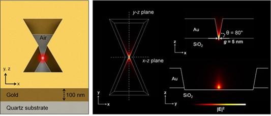
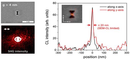
Adopting the proximal focused-ion-beam milling technology, the KAIST research team developed a 3D four nanometer wide gap-plasmon antenna. By squeezing the photons into a 3D nano space of 4 x 10 x 10 nm3 size, the researchers were able to increase the intensity of light by 400,000 times stronger than that of the incident light. Capitalizing on the enhanced intensity of light within the antenna, they intensified the second-harmonic signal and verified that the light was focused in the nano gap by scanning cathodoluminescent images.
The researchers anticipate that this technology will improve the speed of data transfer and processing up to the level of a terahertz (one trillion times per second) and to enlarge the storage volume per unit area on hard disks by 100 times. In addition, high definition images of submolecule size can be taken with actual light, instead of with an electron microscope, while improving the semiconductor process to a smaller size of few nanometers.
Professor Kim said, “A simple yet ingenious idea has shifted the research paradigm from 2D gap-plasmon antennas to 3D antennas. This technology will see numerous applications including in the field of information technology, data storage, imaging medical science, and semiconductor processes.”
The research was sponsored by the National Research Foundation of Korea.
Figure 1: 3D Gap-Plasmon Antenna Structure and Simulation Results

Figure 2 – Constructed 3D Gap-Plasmon Antenna Structure

Figure 3 – Amplified Second Harmonic Signal Generation and Light Focused in the Nano Gap

-
event KAIST ISSS Research Session Captivates 150↑ International Scholars, Achieve Major Success
< Photo. Scholars gatheres for NRF Information Session at Chung Keun Mo Hall > KAIST’s International Office, headed by Vice President Soyoung Kim, successfully organized the ‘NRF Information Session for International Scholars’ on September 11, 2024, in collaboration with the National Research Foundation of Korea (NRF). The event was held at KAIST’s main campus to enourage the international scholar’s active participation in research projects and suppor
2024-09-13 -
research KAIST Research Team Proves How a Neurotransmitter may be the Key in Controlling Alzheimer’s Toxicity
With nearly 50 million dementia patients worldwide, and Alzheimers’s disease is the most common neurodegenerative disease. Its main symptom is the impairment of general cognitive abilities, including the ability to speak or to remember. The importance of finding a cure is widely understood with increasingly aging population and the life expectancy being ever-extended. However, even the cause of the grim disease is yet to be given a clear definition. A KAIST research team in the Departme
2022-07-29 -
people Professor Byungha Shin Named Scientist of the Month
Professor Byungha Shin from the Department of Materials Science and Engineering won the Scientist of the Month Award presented by the Ministry of Science and ICT (MSIT) and the National Research Foundation of Korea (NRF) on May 4. Professor Shin was recognized for his research in the field of next-generation perovskite solar cells and received 10 million won in prize money. To achieve ‘carbon neutrality,’ which many countries across the globe including Korea hope to realize, the
2021-05-07 -
people Professor Bumjoon Kim Named Scientist of the Month
Professor Bumjoon Kim from the Department of Chemical and Biomolecular Engineering won January’s Scientist of the Month Award presented by the Ministry of Science and ICT (MSIT) and the National Research Foundation of Korea (NRF) on January 6. Professor Kim also received 10 million won in prize money. Professor Kim was recognized for his research in the field of fuel cells. Since the first paper on fuel cells was published in 1839 by the German chemist Friedrich Schonbein, there has bee
2021-01-22 -
people Scientist of October: Professor Jungwon Kim
Professor Jungwon Kim from the Department of Mechanical Engineering was selected as the ‘Scientist of the Month’ for October 2020 by the Ministry of Science and ICT and the National Research Foundation of Korea. Professor Kim was recognized for his contributions to expanding the horizons of the basics of precision engineering through his research on multifunctional ultrahigh-speed, high-resolution sensors. He received 10 million KRW in prize money. Professor Kim was selected as th
2020-10-15