research
In recent years, there has been a rise in demand for large amounts of data to train AI models and, thus, data size has become increasingly important over time. Accordingly, solid state drives (SSDs, storage devices that use a semiconductor memory unit), which are core storage devices for data centers and cloud services, have also seen an increase in demand. However, the internal components of higher performing SSDs have become more tightly coupled, and this tightly-coupled structure limits SSD from maximized performance.
On June 15, a KAIST research team led by Professor Dongjun Kim (John Kim) from the School of Electrical Engineering (EE) announced the development of the first SSD system semiconductor structure that can increase the reading/writing performance of next generation SSDs and extend their lifespan through high-performance modular SSD systems.
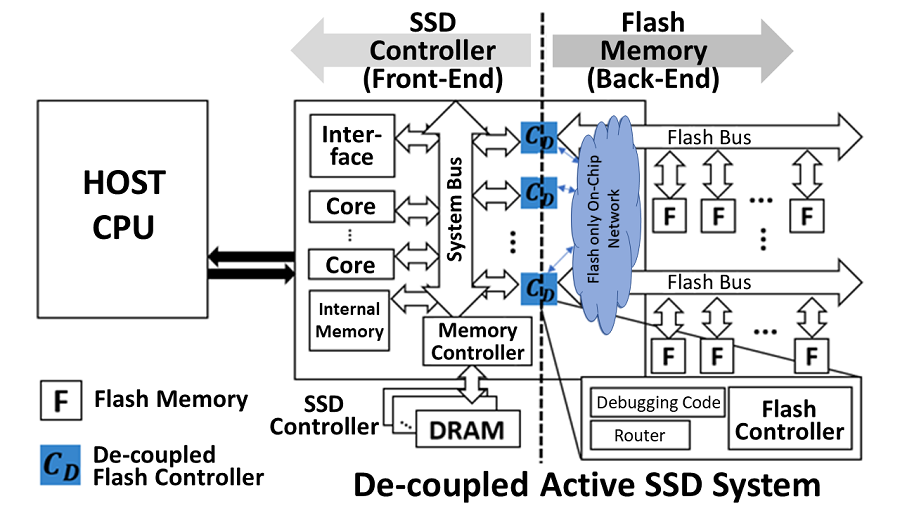
Professor Kim’s team identified the limitations of the tightly-coupled structures in existing SSD designs and proposed a de-coupled structure that can maximize SSD performance by configuring an internal on-chip network specialized for flash memory. This technique utilizes on-chip network technology, which can freely send packet-based data within the chip and is often used to design non-memory system semiconductors like CPUs and GPUs. Through this, the team developed a ‘modular SSD’, which shows reduced interdependence between front-end and back-end designs, and allows their independent design and assembly.
*on-chip network: a packet-based connection structure for the internal components of system semiconductors like CPUs/GPUs. On-chip networks are one of the most critical design components for high-performing system semiconductors, and their importance grows with the size of the semiconductor chip.
Professor Kim’s team refers to the components nearer to the CPU as the front-end and the parts closer to the flash memory as back-end. They newly constructed an on-chip network specific to flash memory in order to allow data transmission between the back-end’s flash controller, proposing a de-coupled structure that can minimize performance drop.
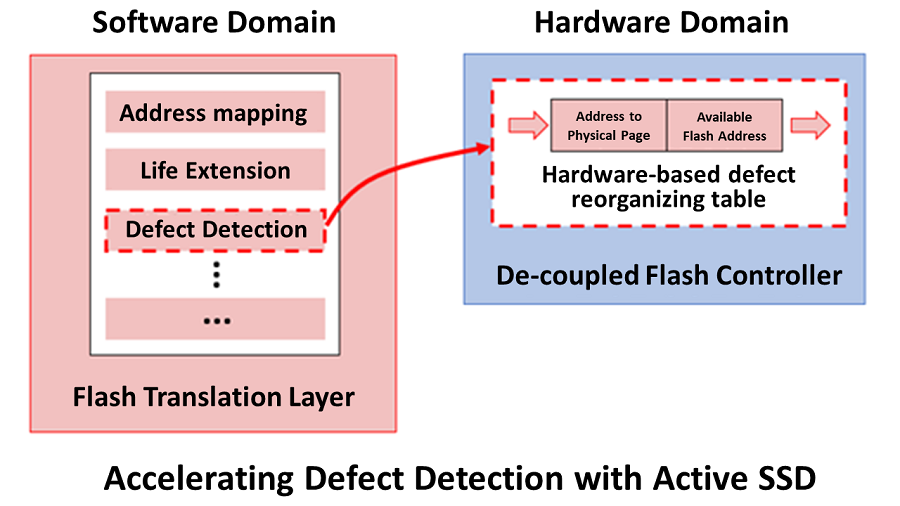
The SSD can accelerate some functions of the flash translation layer, a critical element to drive the SSD, in order to allow flash memory to actively overcome its limitations. Another advantage of the de-coupled, modular structure is that the flash translation layer is not limited to the characteristics of specific flash memories. Instead, their front-end and back-end designs can be carried out independently. Through this, the team could produce 21-times faster response times compared to existing systems and extend SSD lifespan by 23% by also applying the DDS defect detection technique.

< Figure 1. Schematic diagram of the structure of a high-performance modular SSD system developed by Professor Dong-Jun Kim's team >
This research, conducted by first author and Ph.D. candidate Jiho Kim from the KAIST School of EE and co-author Professor Myoungsoo Jung, was presented on the 19th of June at the 50th IEEE/ACM International Symposium on Computer Architecture, the most prestigious academic conference in the field of computer architecture, held in Orlando, Florida. (Paper Title: Decoupled SSD: Rethinking SSD Architecture through Network-based Flash Controllers)

< Figure 2. Conceptual diagram of hardware acceleration through high-performance modular SSD system >
Professor Dongjun Kim, who led the research, said, “This research is significant in that it identified the structural limitations of existing SSDs, and showed that on-chip network technology based on system memory semiconductors like CPUs can drive the hardware to actively carry out the necessary actions. We expect this to contribute greatly to the next-generation high-performance SSD market.” He added, “The de-coupled architecture is a structure that can actively operate to extend devices’ lifespan. In other words, its significance is not limited to the level of performance and can, therefore, be used for various applications.”
KAIST commented that this research is also meaningful in that the results were reaped through a collaborative study between two world-renowned researchers: Professor Myeongsoo Jung, recognized in the field of computer system storage devices, and Professor Dongjun Kim, a leading researcher in computer architecture and interconnection networks.
This research was funded by the National Research Foundation of Korea, Samsung Electronics, the IC Design Education Center, and Next Generation Semiconductor Technology and Development granted by the Institute of Information & Communications Technology, Planning & Evaluation.
- No Data