research

Professor Park Hyun Gyu’s research team from the Department of Chemical and Biomolecular Engineering at KAIST has successfully implemented all logic gates using DNA, a feat that led the research to be published as the cover paper for the international nanotechnology paper "Small".
Even with the latest technology, it was impossible to create a silicon based semiconductor smaller than 10nm, but because DNA has a thickness of only 2nm, this could lead to the creation of semiconductors with groundbreaking degrees of integration.
A 2 nm semiconductor will be able to store 10,000 HD movies within a size of a postage stamp, at least 100 times more than the current 20nm semiconductors.
DNAs are comprised of 4 bases which are continually connected: Adenine (A) with Thymine (T), and Guanine (G) with Cytosine (C).
For this research, the team used the specific binding properties of DNA, which forms its helix-shape, and a circular molecular beacon that has fluorescent signaling properties under structural changes.
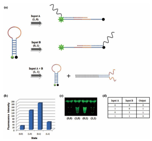
The research team used input signals to open and close the circular DNA, the same principle that is applied to logic gates in digital circuits.
The output signal was measured using the increase and decrease of the fluorescent signal from the molecular beacon due to the opening and closing of the circular DNA respectively.
The team overcame the limited system problems of the existing logic gates and managed to implement all 8 logic gates (AND, OR, XOR, INHIBIT, NAND, NOR, XNOR, IMPlCATION). A multilevel circuit that connects different logic gates was also tested to show its regenerative properties.
Professor Park said that “cheap bio-electric devices with high degrees of integration will be made possible by this research” and that “there will be a large difference in the field of molecular level electronic research”
Mr. Park Gi Su, a doctoral candidate and the 1st author of this research, said that “a DNA sequence of 10 bases is only 3.4nm long and 2nm thick, which can be used to effectively increase the degree of integration of electronic devices” and that “a bio computer could materialize in the near future through DNA semiconductors with accurate logic gates”.
XOR Gate: The output signal 1 comes through the open circular DNA when either input DNA A or input DNA B is present. When both inputs are not present, the flourescent signal does not come through

-
research Highly Uniform and Low Hysteresis Pressure Sensor to Increase Practical Applicability
< Professor Steve Park (left) and the First Author Mr. Jinwon Oh (right) > Researchers have designed a flexible pressure sensor that is expected to have a much wider applicability. A KAIST research team fabricated a piezoresistive pressure sensor of high uniformity with low hysteresis by chemically grafting a conductive polymer onto a porous elastomer template. The team discovered that the uniformity of pore size and shape is directly related to the uniformity of the sensor. The
2019-08-19 -
research A High-Performance and Cost Effective Hydrogen Sensor
(Research team of Professor Park, Professor Jung, and research fellow Gao Min) A KAIST research team reported a high-performance and cost effective hydrogen sensor using novel fabrication process based on the combination of polystyrene nanosphere lithography and semiconductor microfabrication processes. The research team, led by Professor Inkyu Park in the Department of Mechanical Engineering and Professor Yeon Sik Jung in the Department of Materials Science and Engineering, fabricat
2018-05-21 -
people Samsung Electronics' Chairman Kwon Becomes the First Alumnus Honorary Doctorate
(Samsung Electronics' Chairman & CEO Kwon,left, and President Shin) The semiconductor has bred innovation in Korea, as one of the staples of economic growth. Without the success of the semiconductor industry of Korea, it is hard to imagine the high tech dominance in the global market enjoyed by Korean companies. It is said that one in every four Ph.D.s working in the semiconductor industry of Korea graduated from KAIST. Among them, Chairman and CEO Oh-Hyun Kwon of Samsung Electronics
2018-02-26 -
people Professor Lee's Research Selected as Top 100 National R&D Projects
A research project, led by Research Professor Ju Yong Lee from the KAIST Institute for IT Convergence, was selected as one of the Top 100 National Research and Development Projects 2017. This research project, titled LTE-A-based Single RF Small Base Station supporting Multiple Streams, developed 300Mbps low power, low complexity and broadband small base station technology that supports 4x4 MIMO (Multiple Input and Multiple Output) by proposing a new antenna structure and a new RF (Radio Frequ
2017-11-08 -
research KAIST Develops a Method to Transfer Graphene by Stamping
Professor Sung-Yool Choi’s research team from KAIST's Department of Electrical Engineering has developed a technique that can produce a single-layer graphene from a metal etching. Through this, transferring a graphene layer onto a circuit board can be done as easily as stamping a seal on paper. The research findings were published in the January 14th issue of Small as the lead article. This technology will allow different types of wafer transfer methods such as transfer onto a surf
2015-01-23