research
- The first images of mid-infrared optical waves compressed 1,000 times captured using a highly sensitive scattering-type scanning near-field optical microscope. -

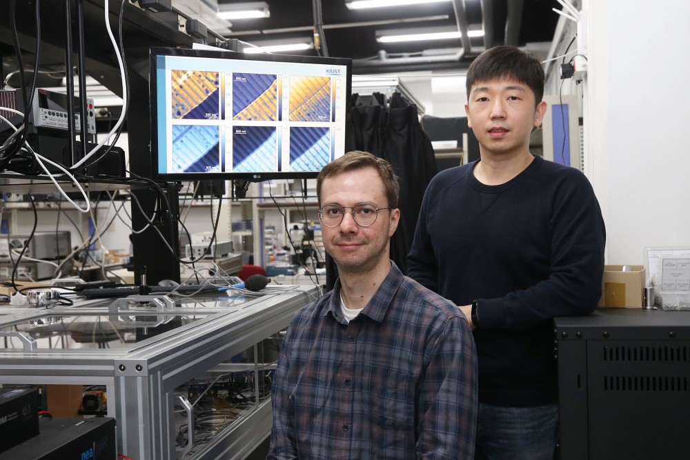
< Post-doc Researcher Sergey G. Menabde (Left) and Professor Min Seok Jang (Right) >
KAIST researchers and their collaborators at home and abroad have successfully demonstrated a new methodology for direct near-field optical imaging of acoustic graphene plasmon fields. This strategy will provide a breakthrough for the practical applications of acoustic graphene plasmon platforms in next-generation, high-performance, graphene-based optoelectronic devices with enhanced light-matter interactions and lower propagation loss.
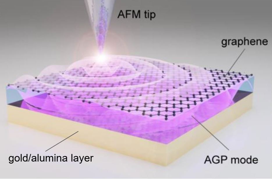
It was recently demonstrated that ‘graphene plasmons’ – collective oscillations of free electrons in graphene coupled to electromagnetic waves of light – can be used to trap and compress optical waves inside a very thin dielectric layer separating graphene from a metallic sheet. In such a configuration, graphene’s conduction electrons are “reflected” in the metal, so when the light waves “push” the electrons in graphene, their image charges in metal also start to oscillate. This new type of collective electronic oscillation mode is called ‘acoustic graphene plasmon (AGP)’.
The existence of AGP could previously be observed only via indirect methods such as far-field infrared spectroscopy and photocurrent mapping. This indirect observation was the price that researchers had to pay for the strong compression of optical waves inside nanometer-thin structures. It was believed that the intensity of electromagnetic fields outside the device was insufficient for direct near-field optical imaging of AGP.
Challenged by these limitations, three research groups combined their efforts to bring together a unique experimental technique using advanced nanofabrication methods. Their findings were published in Nature Communications on February 19.
A KAIST research team led by Professor Min Seok Jang from the School of Electrical Engineering used a highly sensitive scattering-type scanning near-field optical microscope (s-SNOM) to directly measure the optical fields of the AGP waves propagating in a nanometer-thin waveguide, visualizing thousand-fold compression of mid-infrared light for the first time.
Professor Jang and a post-doc researcher in his group, Sergey G. Menabde, successfully obtained direct images of AGP waves by taking advantage of their rapidly decaying yet always present electric field above graphene. They showed that AGPs are detectable even when most of their energy is flowing inside the dielectric below the graphene.
This became possible due to the ultra-smooth surfaces inside the nano-waveguides where plasmonic waves can propagate at longer distances. The AGP mode probed by the researchers was up to 2.3 times more confined and exhibited a 1.4 times higher figure of merit in terms of the normalized propagation length compared to the graphene surface plasmon under similar conditions.
These ultra-smooth nanostructures of the waveguides used in the experiment were created using a template-stripping method by Professor Sang-Hyun Oh and a post-doc researcher, In-Ho Lee, from the Department of Electrical and Computer Engineering at the University of Minnesota.
Professor Young Hee Lee and his researchers at the Center for Integrated Nanostructure Physics (CINAP) of the Institute of Basic Science (IBS) at Sungkyunkwan University synthesized the graphene with a monocrystalline structure, and this high-quality, large-area graphene enabled low-loss plasmonic propagation.
The chemical and physical properties of many important organic molecules can be detected and evaluated by their absorption signatures in the mid-infrared spectrum. However, conventional detection methods require a large number of molecules for successful detection, whereas the ultra-compressed AGP fields can provide strong light-matter interactions at the microscopic level, thus significantly improving the detection sensitivity down to a single molecule.
Furthermore, the study conducted by Professor Jang and the team demonstrated that the mid-infrared AGPs are inherently less sensitive to losses in graphene due to their fields being mostly confined within the dielectric. The research team’s reported results suggest that AGPs could become a promising platform for electrically tunable graphene-based optoelectronic devices that typically suffer from higher absorption rates in graphene such as metasurfaces, optical switches, photovoltaics, and other optoelectronic applications operating at infrared frequencies.
Professor Jang said, “Our research revealed that the ultra-compressed electromagnetic fields of acoustic graphene plasmons can be directly accessed through near-field optical microscopy methods. I hope this realization will motivate other researchers to apply AGPs to various problems where strong light-matter interactions and lower propagation loss are needed.”
This research was primarily funded by the Samsung Research Funding & Incubation Center of Samsung Electronics. The National Research Foundation of Korea (NRF), the U.S. National Science Foundation (NSF), Samsung Global Research Outreach (GRO) Program, and Institute for Basic Science of Korea (IBS) also supported the work.

< Figure. Laser-illuminated nano-tip excites the acoustic graphene plasmon in the layer between the graphene and the gold/alumina. >
Publication:
Menabde, S. G., et al. (2021) Real-space imaging of acoustic plasmons in large-area graphene grown by chemical vapor deposition. Nature Communications 12, Article No. 938. Available online at https://doi.org/10.1038/s41467-021-21193-5
Profile:
Min Seok Jang, MS, PhD
Associate Professor
jang.minseok@kaist.ac.kr
http://jlab.kaist.ac.kr/
Min Seok Jang Research Group
School of Electrical Engineering
http://kaist.ac.kr/en/
Korea Advanced Institute of Science and Technology (KAIST)
Daejeon, Republic of Korea
(END)
-
research KAIST Develops a Fire-risk Free Self-Powered Hydrogen Production System
KAIST researchers have developed a new hydrogen production system that overcomes the current limitations of green hydrogen production. By using a water-splitting system with an aqueous electrolyte, this system is expected to block fire risks and enable stable hydrogen production. KAIST (represented by President Kwang Hyung Lee) announced on the 22nd of October that a research team led by Professor Jeung Ku Kang from the Department of Materials Science and Engineering developed a self-powered hy
2024-10-22 -
research KAIST Develops Stretchable Displays Featuring 25% Expansion Without Image Distortion
Stretchable displays, praised for their spatial efficiency, design flexibility, and human-like flexibility, are seen as the next generation of display technology. A team of Korean researchers has developed a stretchable display that can expand by 25% while maintaining clear image quality without distortion. It can also stretch and contract up to 5,000 times at 15% expansion without any performance degradation, making it the first deformation-free stretchable display with a negative Poisson's rat
2024-09-20 -
research KAIST Research Team Breaks Down Musical Instincts with AI
Music, often referred to as the universal language, is known to be a common component in all cultures. Then, could ‘musical instinct’ be something that is shared to some degree despite the extensive environmental differences amongst cultures? On January 16, a KAIST research team led by Professor Hawoong Jung from the Department of Physics announced to have identified the principle by which musical instincts emerge from the human brain without special learning using an artificial neu
2024-01-23 -
research North Korea and Beyond: AI-Powered Satellite Analysis Reveals the Unseen Economic Landscape of Underdeveloped Nations
- A joint research team in computer science, economics, and geography has developed an artificial intelligence (AI) technology to measure grid-level economic development within six-square-kilometer regions. - This AI technology is applicable in regions with limited statistical data (e.g., North Korea), supporting international efforts to propose policies for economic growth and poverty reduction in underdeveloped countries. - The research team plans to make this technology freely available f
2023-12-07 -
research KAIST builds a high-resolution 3D holographic sensor using a single mask
Holographic cameras can provide more realistic images than ordinary cameras thanks to their ability to acquire 3D information about objects. However, existing holographic cameras use interferometers that measure the wavelength and refraction of light through the interference of light waves, which makes them complex and sensitive to their surrounding environment. On August 23, a KAIST research team led by Professor YongKeun Park from the Department of Physics announced a new leap forward in 3D
2023-09-05