Graduate+School+of+Nanoscience+and+Technology
-
 Observation of the Phase Transition of Liquid Crystal Defects
KAIST researchers observed the phase transition of topological defects formed by liquid crystal (LC) materials for the first time.
The phase transition of topological defects, which was also the theme of the Nobel Prize for Physics in 2016, can be difficult to understand for a layperson but it needs to be studied to understand the mysteries of the universe or the underlying physics of skyrmions, which have intrinsic topological defects.
If the galaxy is taken as an example in the universe, it is difficult to observe the topological defects because the system is too large to observe some changes over a limited period of time. In the case of defect structures formed by LC molecules, they are not only a suitable size to observe with an optical microscope, but also the time period in which the phase transition of a defect occurring can be directly observed over a few seconds, which can be extended to a few minutes. The defect structures formed by LC material have radial, circular, or spiral shapes centering on a singularity (defect core), like the singularity that was already introduced in the famous movie "Interstellar,” which is the center point of black hole.
In general, LC materials are mainly used in liquid crystal displays (LCDs) and optical sensors because it is easy to control their specific orientation and they have fast response characteristics and huge anisotropic optical properties. It is advantageous in terms of the performance of LCDs that the defects of the LC materials are minimized. The research team led by Professor Dong Ki Yoon in the Graduate School of Nanoscience and Technology did not simply minimize such defects but actively tried to use the LC defects as building blocks to make micro- and nanostructures for the patterning applications. During these efforts, they found the way to directly study the phase transition of topological defects under in-situ conditions.
Considering the LC material from the viewpoint of a device like a LCD, robustness is important. Therefore, the LC material is injected through the capillary phenomenon between a rigid two-glass plate and the orientation of the LCs can be followed by the surface anchoring condition of the glass substrate. However, in this conventional case, it is difficult to observe the phase transition of the LC defect due to this strong surface anchoring force induced by the solid substrate.
In order to solve this problem, the research team designed a platform, in which the movement of the LC molecules was not restricted, by forming a thin film of LC material on water, which is like oil floating on water. For this, a droplet of LC material was dripped onto water and spread to form a thin film. The topological defects formed under this circumstance could show the thermal phase transition when the temperature was changed. In addition, this approach can trace back the morphology of the original defect structure from the sequential changes during the temperature changes, which can give hints to the study of the formation of topological defects in the cosmos or skyrmions.
Prof. Yoon said, “The study of LC crystal defects itself has been extensively studied by physicists and mathematicians for about 100 years. However, this is the first time that we have observed the phase transition of LC defects directly.” He also added, "Korea is leading in the LCD industry, but our basic research on LCs is not at the world's research level."
The first author of this study is Dr. Min-Jun Gimand supported by a grant from the National Research Foundation (NRF) and funded by the Korean Government (MSIP). The research result was published on May 30, 2017 in Nature Communications.
Figure 1. The phase transition of the LC topological defect on cooling.
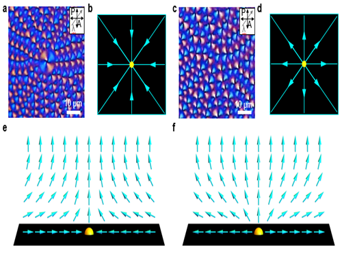
Figure 2. Polarizing optical microscopy images of topological defects depending on the strength of the director field. (a,b,e) Convergent director field arrangements of LC molecules and corresponding schematic images; (c,d,f) Divergent director field arrangements of LC molecules and corresponding schematic images.
2017.06.02 View 8686
 -
 Scholarship in Memory of Professor Shin Endowed by His Family
Professor Joong-Hoon Shin of the Graduate School of Nanoscience and Technology was touted as a genius young scientist who would take the lead in nanoscience technology. After earning degrees from Harvard and the Caltech, he was appointed at KAIST at age 27. He was the youngest professor ever appointed in Korea.
Professor Shin’s outstanding research in the field of semiconductor nano-optics led him to be named as the ‘Scientist of the Year’ for three consecutive years from 2004 by the most prestigious scientist and technology organizations including the Korean Academy Science and Technology, the National Research Foundation of Korea, and the Korean government. However, a fatal car accident last September on the way home from a seminar in Gangwon Province took his life and a promising scholar’s research was left unfinished. He was 47 years old.
Mrs. Young-Eun Hong, the widow of the late Professor Shin, made a 100 million KRW gift to KAIST to establish the ‘Joong-Hoon Shin Scholarship’ on April 7. The scholarship will provide financial assistance to outstanding students of physics and nanoscience.
At the donation ceremony attended by President Sung-Chul Shin, Professor Shin’s colleagues and students, and family members, Mrs. Hong said, “My family would like to help young students achieve their dreams on behalf of my husband. I hope students will remember my husband’s passion and dedication toward his studies for a long time. He was a very hard worker.”
Working at KAIST, Professor Shin made significant achievements in field of semiconductor nano-optics, specializing in silicon photonics and silicon nanocrystal structures. In particular, his research team gained attention reproducing the structure of ‘Morpho butterfly’ wings, which produce the same colors from various angles, using external light as a light source without extra power. Their research led to the creation of original technology dubbed the biomimetics reflective display and was published in Nature in 2012.
Professor Shin’s legacy still endures. In February, a research team under Professor Shin-Hyun Kim of the Department of Chemical and Biomolecular Engineering includingthe late Professor Shin’s doctoral student Seung Yeol Lee, posthumously dedicated their research published on Advanced Materials to Professor Shin. ( click )
KAIST President Sung-Chul Shin, who is also a physicist, said “His passing is a great loss to the whole scientific and technology community, at home and abroad. But Joong-Hoon Shin scholarship will enable the growth and ensure the strength of nanoscience and its education at KAIST. We will uphold Professor Shin’s legacy by doing our best to make KAIST a world-leading university which can create global value.”
Mrs. Hong said she will continue her husband’s academic legacy at his alma maters, Harvard and the Caltech, where he earned his BS in physics and his Ph.D. in applied physics respectively. She said she will start fundraising to establish the Joong-Hoon Shin Scholarship at Harvard and Caltech from July.
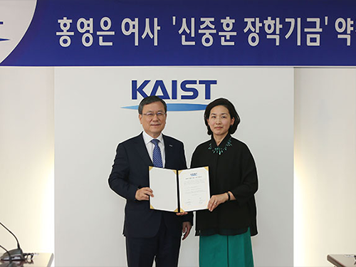
(Mrs. Hong poses with President Sung-Chul Shin after donating 100 million KRW for establishing 'Joong-Hoon Shin Scholarship' in memory of her husband on April 7.)
2017.04.10 View 6831
 -
 Controlling DNA Orientation Using a Brush
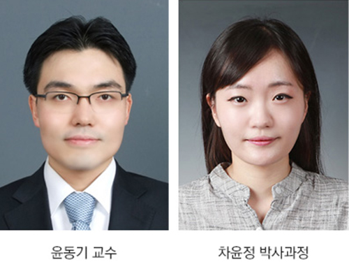
Professor Dong Ki Yoon’s research team in the Graduate School of Nanoscience and Technology has developed a technique for producing periodic DNA zigzag structures using a common make-up brush.
The results of the research, first-authored by Ph.D. student Yun Jeong Cha and published in Advanced Materials (online, November 15, 2016), has been highlighted in the hot topics of “Liquid Crystals.”
There exist various methods for synthesizing DNA-based nanostructures, but they commonly involved complex design processes and required expensive DNA samples with regulated base sequences.
Using DNA materials extracted from salmon, the research team was able to produce a nanostructure with a well-aligned zigzag pattern at one-thousandth of the usual cost.
The team used a commercial make-up brush bought at a cosmetics store, and with it, applied the salmon DNA in one direction onto a plate, in the same way paint is brushed onto paper. Using a brush with a width of several centimeters, the team aligned DNA molecules of 2 nanometers in diameter along the direction of the brush strokes.
As the thin and dense film of DNA came into contact with air, it lost moisture. An expansive force was created between the dried film and the plate. This force interacted with the elastic force of DNA and caused undulations in the uni-directionally aligned DNA molecules, which resulted in a regular zigzag pattern.
The zigzag DNA’s base sequences could not be controlled because it was extracted from biological sources. However, it has the advantage of being cheap and readily available without compromising its structural integrity and provides a very regular and intricate structure.
This kind of well-ordered DNA structure can be used as template because it can guide or control versatile guest functional materials that are applied to its surface. For example, it can align liquid crystals used in displays, as well as metallic particles and semi-conductors. It is expected that this capacity can be extended to optoelectric devices in the future.
Professor Yoon remarked that “these findings have special implications, as they have demonstrated that various materials in nature aside from DNA, such as proteins, muscle cells, and components of bones can be applied to optoelectric devices.”
This research has been carried out with the support of the Korea National Research Foundation’s Nanomaterials Fundamental Technology Development Program and the Pioneer Research Center under the High-tech Convergence Technology Development Program.
Source: "Control of Periodic Zigzag Structures of DNA by a Simple Shearing Method" by Yun Jeong Cha and Dong Ki Yoon (Advanced Materials, November 15, 2016, DOI: 10.1002/adma.201604247)
Figure 1. Diagram showing the well-ordered zigzag structure of DNA, and the internal molecular orientation
Figure 2. (Left) Unaligned DNA (Right) Aligned DNA after being brushed and dried
Figure 3. Control of the periodicity of the DNA zigzag patterns using micro-channel plates
Figure 4. Diagram representing the control of orientation of liquid crystal materials applied on a zigzag DNA template, and a polarized optical microscope image
2017.01.10 View 6466
 -
 Hierarchically-Porous Polymers with Fast Absorption
KAIST's Professor Myungeun Seo and his research team from the Graduate School of Nanoscience and Technology has developed a method to form micropores of less than 2 nanometers within porous polymers where 10 nanometers long mesopores connect like a net. The advantage of the porous polymers is fast absorption of molecules.
Porous polymers with micropores of less than 2 nanometers, like a zeolite, have a large surface area. They are used as a means to store hydrogen-based molecules or as a catalytic support that can be used as a surface to convert a material into a desired form. However, because the size of the pores in its path was too small for the molecules, it took a long time to spread into the pores and reach the surface.
To reach the surface efficiently, a lung cell or the vein of a leaf has a structure wherein the pores are subdivided into different sizes so that the molecule can spread throughout the organ. A technology that can create not only micropores but also bigger pores was necessary in order to create such structure.
The research team solved the issue by implementing a "self-assembly" of block polymers to easily form a net-like nanostructure from mesopores of 10 nanometers.
The team created hierarchically-porous polymers consisting of two different types of pores by using a hypercrosslinking reaction along with the "self-assembly" method. The reaction creates micropores within the chain after the polymer chain is confined by a chemical bond.
This porous polymer has micropores that are smaller than 2 nanometers on the walls of mesopores while 10 nanometers long mesopores forming 3-dimensional net structures. Because of the "self-assembly" method, the size of mesopores can be adjusted within the range of 6 to 15 nanometers.
This is the first case where a porous polymer has both well-defined mesopores and micropores. The research team verified the effect of hierarchically-porous structures on absorption of molecules by confirming that the porous polymer had faster absorption speeds than a polymer consisting only of micropores.
Professor Seo said, “The study has found a simple way to create different sizes of pores within a polymer.” He expected that the hierarchically-porous polymers can be used as a catalytic support in which fast diffusion of molecules is essential, or for molecule collection.
The research was sponsored by National Research Foundation of Korea and published online in the Journal of the American Chemical Society.
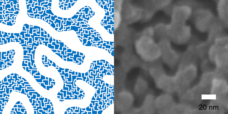
Figure 1 – Net-like Structure of Hierarchically-Porous Polymers with Mesopores and Micropores on the walls of Mesopores.
Figure 2 - Hierarchically-Porous Polymers
Figure 3 – Comparison of Porous-Polymers consisting of Mesopores only (left), and Mesopores and Micropores (right)
2015.01.13 View 8063
 -
 KAIST Develops Core Technology to Synthesize a Helical Nanostructure
Professor Dong-Ki Yoon’s research team of the Graduate School of Nanoscience and Technology (GSNT) at KAIST has developed helical nanostructures using self-assembly processes. The results were published in the Proceedings of the National Academy of Sciences of the United States of America(PNAS) on the October 7th.
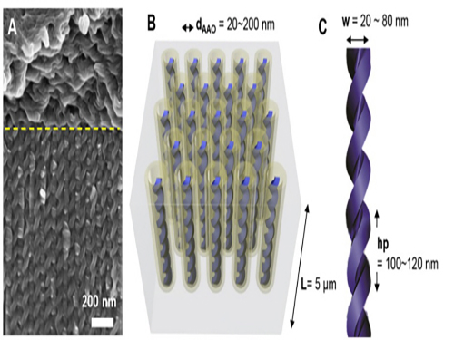
This technology enables the synthesis of various helical structures on a relatively large confined area. Its synthesis is often considered the most arduous for three dimensional structures. Formed from liquid crystal, the structure holds a regular helical structure within the confined space of 20 to 300 nanometers. Also, the distance between each pattern increased as the diameter of the nanostructure increased.
Liquid crystals have a unique property of responding sensitively to the surrounding electromagnetic field. The technology, in combination with the electromagnetic property of liquid crystal, is expected to foster the development of highly efficient optoelectronic devices.
Using this technology, it is possible to develop three dimensional patterning technology beyond the current semiconductor manufacturing technology which uses two dimensional photolithography processes. Three-dimensional semiconductor devices are expected to store hundred times more data than current devices. They will also lower costs by simplifying manufacturing processes.
The essence of this research, “self-assembly in confined space,” refers to controlling complex nanostructures, which can be synthesized from materials such as macromolecules, liquid crystal molecules, and biomolecules in relation to surrounding environments including the temperature, concentration, and pH.
The research team produced a confined space with a length of tens of nanometers by using a porous anodized aluminum membrane induced from an electrochemical reaction. They successfully synthesized independently controlled helical nanostructures by forming the helical structures from liquid crystal molecules within that space.
Professor Yoon said, “This research examines the physicochemical principle of controlling helical nanostructures.” He highlighted the significance of the research and commented, “The technology enables the control of complex nanostructures from organic molecules by using confined space and surface reforming.”
He added that, “When grafted with nanotechnology or information technology, this technology will spur new growth to liquid crystal-related industries such as the LCD.”
The research was led by two Ph.D. candidates, Hanim Kim and Sunhee Lee, under the guidance of Professor Yoon. Dr. Tae-Joo Shin of the Pohang Accelerator Laboratory, Professor Sang-Bok Lee of the University of Maryland, and Professor Noel Clark of the University of Colorado also participated.
Picture 1. Electron Microscopy Pictures and Conceptual Diagrams of Helical Nanostructures
Picture 2. Electron Microscopy Pictures of Manufactured Helical Nanostructures
2014.10.29 View 8274
 -
 First Instance of Negative Effects from Terahertz-Range Electromagnetic Waves
Professor Philhan Kim
Electromagnetic waves (EM-wave) in the terahertz range were widely regarded as the “dream wavelength” due to its perceived neutrality. Its application was also wider than X-rays. However, KAIST scientists have discovered negative effects from terahertz EM-waves.
Professor Philhan Kim of KAIST’s Graduate School of Nanoscience and Technology and Dr. Young-wook Jeong of the Korea Atomic Energy Research Institute (KAERI) observed inflammation of animal skin tissue when exposed to terahertz EM-waves.
The results were published in the online edition of Optics Express (May 19, 20104).
Terahertz waves range from 0.1 to 10 terahertz and have a longer wavelength than visible or infrared light. Commonly used to see through objects like the X-ray, it was believed that the low energy of terahertz waves did not inflict any harm on the human body.
Despite being applied for security checks, next-generation wireless communications, and medical imaging technology, little research has been conducted in proving its safety and impact. Conventional research failed to predict the exact impact of terahertz waves on organic tissues as only artificially cultured cells were used.
The research team at KAERI developed a high power terahertz EM-wave generator that can be used on live organisms. A high power generator was necessary in applications such as biosensors and required up to 10 times greater power than currently used telecommunications EM-wave. Simultaneously, a KAIST research team developed a high speed, high resolution video-laser microscope that can distinguish cells within the organism.
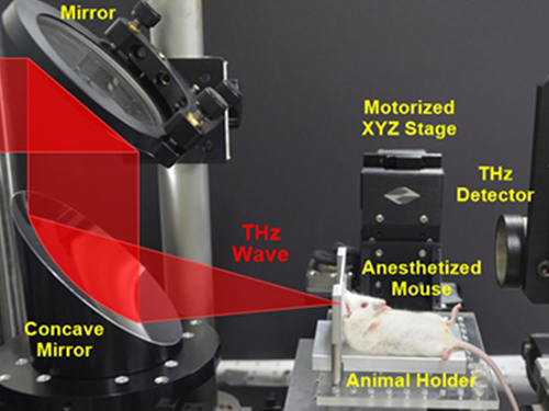
The experiment exposed 30 minutes of terahertz EM-wave on genetically modified mice and found six times the normal number of inflammation cells in the skin tissue after six hours. It was the first instance where negative side effects of terahertz EM-wave were observed.
Professor Kim commented that “the research has set a standard for how we can use the terahertz EM-wave safely” and that “we will use this research to analyze and understand the effects of other EM-waves on organisms.”
2014.06.20 View 8764