Nanowires
-
 Transfering Nanowires onto a Flexible Substrate
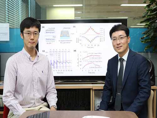
(from left: PhD Min-Ho Seo and Professor Jun-Bo Yoon)
Boasting excellent physical and chemical properties, nanowires (NWs) are suitable for fabricating flexible electronics; therefore, technology to transfer well-aligned wires plays a crucial role in enhancing performance of the devices. A KAIST research team succeeded in developing NW-transfer technology that is expected to enhance the existing chemical reaction-based NW fabrication technology that has this far showed low performance in applicability and productivity.
NWs, one of the most well-known nanomaterials, have the structural advantage of being small and lightweight. Hence, NW-transfer technology has drawn attention because it can fabricate high-performance, flexible nanodevices with high simplicity and throughput.
A conventional nanowire-fabrication method generally has an irregularity issue since it mixes chemically synthesized nanowires in a solution and randomly distributes the NWs onto flexible substrates. Hence, numerous nanofabrication processes have emerged, and one of them is master-mold-based, which enables the fabrication of highly ordered NW arrays embedded onto substrates in a simple and cost-effective manner, but its employment is limited to only some materials because of its chemistry-based NW-transfer mechanism, which is complex and time consuming. For the successful transfer, it requires that adequate chemicals controlling the chemical interfacial adhesion between the master mold, NWs, and flexible substrate be present.
Here, Professor Jun-Bo Yoon and his team from the School of Electrical Engineering introduced a material-independent mechanical-interlocking-based nanowire-transfer (MINT) method to fabricate ultralong and fully aligned NWs on a large flexible substrate in a highly robust manner.
This method involves sequentially forming a nanosacrificial layer and NWs on a nanograting substrate that becomes the master mold for the transfer, then weakening the structure of the nanosacrificial layer through a dry etching process. The nanosacrificial layer very weakly holds the nanowires on the master mold. Therefore, when using a flexible substrate material, the nanowires are very easily transferred from the master mold to the substrate, just like a piece of tape lifting dust off a carpet.
This technology uses common physical vapor deposition and does not rely on NW materials, making it easy to fabricate NWs onto the flexible substrates.
Using this technology, the team was able to fabricate a variety of metal and metal-oxide NWs, including gold, platinum, and copper – all perfectly aligned on a flexible substrate. They also confirmed that it can be applied to creating stable and applicable devices in everyday life by successfully applying it to flexible heaters and gas sensors.
PhD Min-Ho Seo who led this research said, “We have successfully aligned various metals and semiconductor NWs with excellent physical properties onto flexible substrates and applied them to fabricated devices. As a platform-technology, it will contribute to developing high-performing and stable electronic devices.”
This research was published in ACS Nano on May 24.
Figure 1. Photograph of the fabricated wafer-scale fully aligned and ultralong Au nanowire array on a flexible substrate
2018.09.17 View 6811
 -
 Improving Silver Nanowires for FTCEs with Flash Light Interactions
Flexible transparent conducting electrodes (FTCEs) are an essential element of flexible optoelectronics for next-generation wearable displays, augmented reality (AR), and the Internet of Things (IoTs). Silver nanowires (Ag NWs) have received a great deal of attention as future FTCEs due to their great flexibility, material stability, and large-scale productivity. Despite these advantages, Ag NWs have drawbacks such as high wire-to-wire contact resistance and poor adhesion to substrates, resulting in severe power consumption and the delamination of FTCEs.
A research team led by Professor Keon Jae Lee of the Materials Science and Engineering Department at KAIST and Dr. Hong-Jin Park from BSP Inc., has developed high-performance Ag NWs (sheet resistance ~ 5 Ω/sq, transmittance 90 % at λ = 550 nm) with strong adhesion on plastic (interfacial energy of 30.7 J∙m-2) using flash light-material interactions.
The broad ultraviolet (UV) spectrum of a flash light enables the localized heating at the junctions of nanowires (NWs), which results in the fast and complete welding of Ag NWs. Consequently, the Ag NWs demonstrate six times higher conductivity than that of the pristine NWs. In addition, the near-infrared (NIR) of the flash lamp melted the interface between the Ag NWs and a polyethylene terephthalate (PET) substrate, dramatically enhancing the adhesion force of the Ag NWs to the PET by 310 %.
Professor Lee said, “Light interaction with nanomaterials is an important field for future flexible electronics since it can overcome thermal limit of plastics, and we are currently expanding our research into light-inorganic interactions.”
Meanwhile, BSP Inc., a laser manufacturing company and a collaborator of this work, has launched new flash lamp equipment for flexible applications based on the Professor Lee’s research.
The results of this work entitled “Flash-Induced Self-Limited Plasmonic Welding of Ag NW Network for Transparent Flexible Energy Harvester (DOI: 10.1002/adma.201603473)” were published in the February 2, 2017 issue of Advanced Materials as the cover article.
Professor Lee also contributed an invited review in the same journal of the April 3, 2017 online issue, “Laser-Material Interactions for Flexible Applications (DOI:10.1002/adma.201606586),” overviewing the recent advances in light interactions with flexible nanomaterials.
References
[1] Advanced Materials, February 2, 2017, Flash-Induced Self-Limited Plasmonic Welding of Ag NW network for Transparent Flexible Energy Harvester http://onlinelibrary.wiley.com/doi/10.1002/adma.201603473/epdf
[2] Advanced Materials, April 3, 2017, Laser-Material Interactions for Flexible Applications
http://onlinelibrary.wiley.com/doi/10.1002/adma.201606586/abstract
For further inquiries on research:
keonlee@kaist.ac.kr (Keon Jae Lee), hjpark@bsptech.co.kr (Hong-Jin Park)
Picture 1: Artistic Rendtition of Light Interaction with Nanomaterials
(This image shows flash-induced plasmonic interactions with nanowires to improve silver nanowires (Ag NWs).)
Picture 2: Ag NW/PET Film
(This picture shows the Ag NWs on a polyethylene terephthalate (PET) film after the flash-induced plasmonic thermal process.)
2017.04.05 View 11700