ANG
-
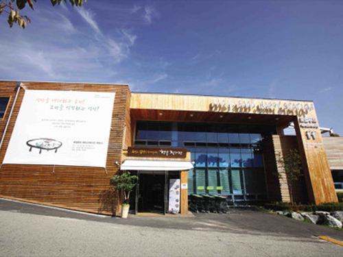 KAIST Develops IoT Platform for Food Safety
A research team led by the KAIST Auto-ID Labs developed a GS1 international standard-based IoTs infrastructure platform dubbed Oliot (Open Language of Internet of Things). This platform will be applied to Wanju Local Food, the nation’s largest cooperative, and will be in operation from April 5.
A total of eleven organizations participated in the development of Oliot, with KAIST as the center. This consortium is based on the GS1 international standard-based Oliot platform, which allows collecting and sharing data along the entire process of agrifood from production to processing, distribution, and consumption. It aims at increasing farm incomes and establishing a global ecosystem of domestic agriculture and stockbreeding that provides safe food.
Wanju Local Food is now the world’s first local food co-op with a traceability system from the initial stage of production planning to end sales based on GS1 international standards, which will ensure food safety.
KAIST has been sharing Oliot data in order to apply it to industries around the world. As of April 2018, approximately 900 enterprises and developers from more than 100 countries have downloaded it.
Professor Daeyoung Kim from the School of Computing, who is also Research Director of Auto-ID Labs said, “We are planning to disseminate Oliot to local food cooperatives throughout the nation. We will also cooperate with other countries, like China, Holland, and Hong Kong to create a better ecosystem for the global food industry.
“We are currently collaborating with related business to converge Oliot with AI or blockchain technology that can be applied to various services, such as healthcare and smart factories. Its tangible outcome will be revealed soon,” he added.
Auto-ID Labs are a global research consortium of six academic institutions that research and develop new technologies for advancing global commerce, partnering with GS1 (Global Standard 1), a non-profit organization that established standards for global commerce such as introducing barcodes to the retail industry. The Auto-ID Labs include MIT, University of Cambridge, Keio University, Fudan University, ETH Zurich/University of St. Gallen, and KAIST.
The consortium was supported by the Ministry of Science and ICT as well as the Institute for Information and Communications Technology Promotion for three years from 2015.
The launching of Oliot at Wanju Local Food will be held on April 5.
2018.04.03 View 9086
 -
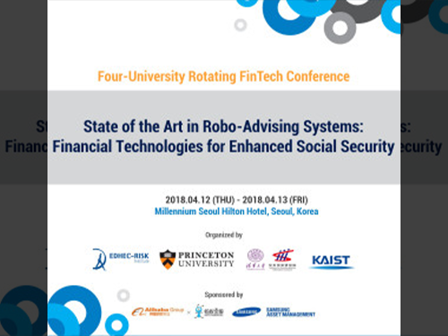 KAIST to Host FinTech Conference 2018
KAIST will be hosting a FinTech Conference with Princeton University (USA), Tsinghua University (China), and EDHEC Business School (France) in Seoul from April 12 to 13 titled State of the Art in Robo-Advising Systems: Financial Technologies for Enhanced Social Security.
The Bendhein Center for Finance and Department of Operations Research and Financial Engineering from Princeton University, Fintech Lab from Tsinghua University, and the Risk Institute from EDHEC will participate as co-hosting organizations in this conference organized by the Department of Industrial & Systems Engineering and the KAIST Center for Wealth Management Technologies.
The conference will discuss issues required for providing customized asset management to the public in terms of theory, technology, and industry.
During the conference, KAIST President Sung-Chul Shin and Chairman and CEO of the National Pension Service Sung Joo Kim will deliver welcoming addresses.
Professor John Mulvey from Princeton University, Professor Michael Dempster from Cambridge University, Professors Wei Xu and Changle Lin from Tsinghua University, Professor Lionel Martellini from EDHEC, and Professor Woo Chang Kim from KAIST are some of the invited speakers at the event.
Moreover, renowned experts in related fields will also participate in the conference, including Founder of Vanguard Group John Bogle, Jin Lee from Ant Financial, Youngsuh Cho from Shinhan Financial Group, Jung-Hwan Lee from Samsung Asset Management, and Hye Young Sung from the National Pension Service Research Institute.
Professor Kim said, “Only a small number of wealthy people can receive life-cycle customized asset management services due to the high cost structure; however, new technology derived from the Fourth Industrial Revolution can reduce the service price in an innovative manner, ultimately leading it to be popularized.”
“In an era with the poverty rate of older people reaching almost 50%.Fintech can enable individuals to manage their assets in an active manner, reinforcing social security without additional social costs in the period,” he added.
These four universities have been hosting the FinTech Conference since 2017. China will host the conference this fall, followed by France next year.
Samsung Asset Management, Alibaba Group, and Ant Financial will sponsor the conference. Anyone interested in this event can find more details at http://wmt.kaist.ac.kr/conference.html.
2018.04.02 View 8099
 -
 Open Online Course in Science and Technology, STAR-MOOC
Four universities specializing in science and technology, along with POSTECH and UST, teamed up to establish programs for innovation in education programs, responding to the Fourth Industrial Revolution.
KAIST held an opening ceremony for the Science & Technology Advanced Research - Massive Open Online Course (STAR-MOOC) and signed an MoU with GIST, DGIST, UNIST, POSTECH, and UST.
STAR-MOOC was launched on February 26 to provide educational service to the public. It is a joint platform where people can take courses featuring lectures from professors from universities specializing in science and technology as well as national research universities.
It offers 15 courses covering basics, majors, and electives related to science and technology developed by the STAR-MOOC committee. Students can take a variety of courses.
At the opening ceremony, KAIST President Sung-Chul Shin, DGIST President Sang Hyuk Son, UST President Kil Choo Moon, POSTECH Vice President Wankyun Chung, UNIST Vice President Jae Sung Lee, GIST Vice President of Public Affairs Pil-hwan Park came to sign the MoU for provising educational services for the public.
During the ceremony, there was also time to introduce a technical agreement with a non-profit organization founded by NAVER, the CONNECT Foundation, for its courses and platform.
Universities participating in STAR-MOOC will put effort into capacity building in response to changes driven by the Fourth Industrial Revolution.
President Shin said, “STAR-MOOC is a platform that provides science and technology courses from basics to electives and major courses. It will become a leading educational platform.”
Students can register and choose courses from the website (http://starmooc.kr).
2018.03.19 View 8476
 -
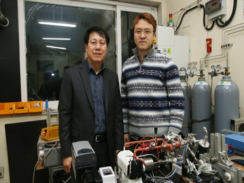 KAIST Finds the Principle of Electric Wind in Plasma
(From left: Professor Wonho Choe and PhD Sanghoo Park)
A KAIST team identified the basic principle of electric wind in plasma. This finding will contribute to developing technology in various applications of plasma, including fluid control technology.
Professor Wonho Choe from the Department of Physics and his team identified the main principle of neutral gas flow in plasma, known as ‘electric wind’, in collaboration with Professor Se Youn Moon’s team at Chonbuk National University.
Electric wind in plasma is a well-known consequence of interactions arising from collisions between charged particles (electrons or ions) and neutral particles. It refers to the flow of neutral gas that occurs when charged particles accelerate and collide with a neutral gas.
This is a way to create air movement without mechanical movement, such as fan wings, and it is gaining interest as a next-generation technology to replace existing fans. However, there was no experimental evidence of the cause.
To identify the cause, the team used atmospheric pressure plasma. As a result, the team succeeded in identifying streamer propagation and space charge drift from electrohydrodynamic (EHD) force in a qualitative manner.
According to the team, streamer propagation has very little effect on electric wind, but space charge drift that follows streamer propagation and collapse was the main cause of electric wind.
The team also identified that electrons, instead of negatively charged ions, were key components of electric wind generation in certain plasmas.
Furthermore, electric wind with the highest speed of 4 m/s was created in a helium jet plasma, which is one fourth the speed of a typhoon. These results indicate that the study could provide basic principles to effectively control the speed of electric wind.
Professor Choe said, “These findings set a significant foundation to understand the interactions between electrons or ions and neutral particles that occur in weakly ionized plasmas, such as atmospheric pressure plasmas. This can play an important role in expanding the field of fluid-control applications using plasmas which becomes economically and commercially interest.”
This research, led by PhD Sanghoo Park, was published online in Nature Communications on January 25.
Figure 1. Plasma jet image
Figure 2. The differences in electric wind speeds and voltage pulse
2018.03.02 View 7619
 -
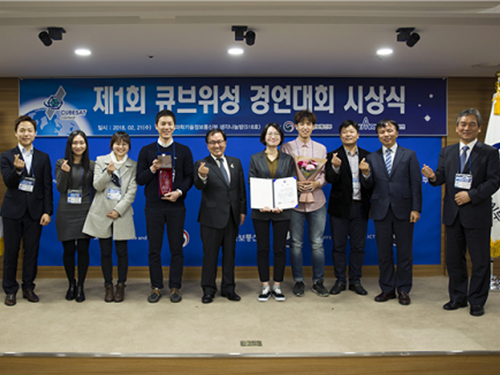 KAIST, First to Win the Cube Satellite Competition
Professor Hyochoong Bang from the Department of Aerospace Engineering and his team received the Minister of Science and ICT Award at the 1st Cube Satellite Competition.
The team actually participated in the competition in 2012, but it took several years for the awarding ceremony since it took years for the satellites to be designed, produced, and launched.
The KAIST team successfully developed a cube satellite, named ‘Little Intelligent Nanosatellite of KAIST (LINK)’ and completed its launch in April 2017.
LINK (size: 20cmx10cmx10cm, weight: 2kg) mounted mass spectrometry and Langmuir probe for Earth observation. The Langmuir probe was developed by Professor Kyoung Wook Min from the Department of Physics, KAIST.
Yeerang Lim, a PhD student from the Department of Aerospace Engineering said, “I still remember the feeling that I had on the day when LINK launched into orbit and sent back signals. I hope that space exploration is not something far away but attainable for us in near future.”
2018.02.22 View 10999
 -
 First Female Grand Prize Awardee of Samsung Humantech
Yeunhee Huh, PhD candidate (Professor Gyu-Hyeong Cho) from the School of Electrical Engineering received the grand prize of the 24th Humantech Paper Award. She is the first female recipient of this prize since its establishment in 1994. The Humantech Paper Award is hosted by Samsung Electronics and sponsored by the Ministry of Science and ICT with JoongAng Daily Newspaper. Her paper is titled, ‘A Hybrid Structure Dual-Path Step-Down Converter with 96.2% Peak Efficiency using 250mΩ Large-DCR Inductor’. Electronic devices require numerous chips and have a power converter to supply energy adequately. She proposed a new structure to enhance energy efficiency by combining inductors and capacitors. Enhancing energy efficiency can reduce energy loss, which prolongs battery hours and solves overheating of devices; for instance, energy loss leads to the overheating issue affecting phone chargers. This technology can be applied to various electronic devices, such as cell phones, laptops, and drones. Huh said, “Power has to go up in order to meet customers’ needs; however the overheating problem emerges during this process. This problem affects surrounding circuits and causes other issues, such as malfunctions of electronic devices. This technology may vary according to the conditions, but it can enhance energy efficiency up to 4%.”During the ceremony, about eight hundred million KRW worth cash prizes was conferred to 119 papers. KAIST (44 papers) and Gyeonggi Science High School (6 papers) received special awards given to the schools.
2018.02.12 View 9058
 -
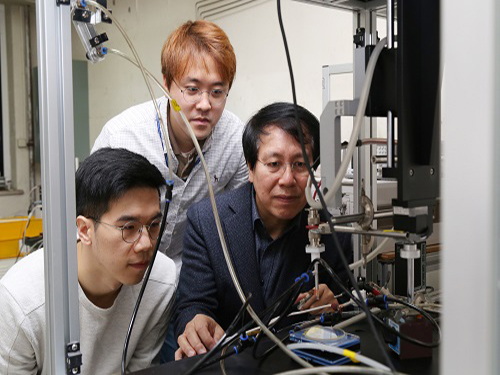 Plasma, an Excellent Sterilizer to Remove Harmful Bacteria
(PhD candidate Joo Young Park, Professor Wonho Choe and PhD researcher Sanghoo Park)
KAIST researchers are using plasma to remove bacteria that are stuck to surfaces of plastic bottles and food. This novel technology will contribute to disinfection in medical settings as well as food and agricultural industries.
Professor Wonho Choe and his team from the Department of Physics developed a technology that removes biofilm, which is comprised of microorganisms, by using plasma as a non-thermal sterilization method.
Plasma contains multiple bactericidal agents, including reactive species. In particular, the chemicals formed in aqueous solution during plasma exposure have the potential for high antibacterial activity against various bacterial infections.
The team treated water with plasma to see how effectively bactericidal agents in the plasma water can remove biofilm comprised of harmful microorganism such as Escherichia coli, Salmonella, and Listeria.
The team identified that reactive species, including hydroxyl radical, hydrogen peroxide, ozone, nitrite, and superoxide produced during plasma treatment, showed considerable ability to remove the biofilm. Hydrogen peroxide showed the strongest effect removing the biofilm; however, the hydroxyl radical also played a significant role in removing biofilm. Despite having a concentration 100 to 10,000 times lower than other reactive species, the hydroxyl radical showed a high biofilm removal efficacy owing to its strong oxidative power.
These findings reveal that plasma can be used as a no-residual and safe sterilization process alternative to conventional methods. With these outcomes, the team is planning to develop and commercialize a technology that can produce hydroxyl radicals with plasma.
Professor Choe has registered a patent for flexible packaging materials that facilitate plasma and completed the technology transfer to the startup company, named ‘Plasmapp’, which focuses on commercializing bactericidal technology.
“This research outcome will be the foundation for understanding plasma control technology and physicochemical interactions between plasma and microorganisms. It will also become an accelerator for utilizing plasma technology in the medical, food, and agricultural fields,” said Professor Choe.
This research, led by PhD candidate Joo Young Park and PhD researcher Sanghoo Park in collaboration with Professor Cheorun Jo’s team from Seoul National University, was published in ACS Applied Materials and Interfaces on December 20, 2017.
Figure 1. Flexible packaging materials that facilitate plasma
Figure 2. Schematic diagram of biofilm treatment with plasma
Figure 3. Concept of plasma application and evaluation result of reactive species' efficacy
Figure 4. STERPACK, the product launched by Plasmapp
2018.01.25 View 9610
 -
 Three Professors Named KAST Fellows
(Professor Dan Keun Sung at the center)
(Professor Y.H. Cho at the center)
(Professor K.H. Cho at the center)
The Korean Academy of Science and Technology (KAST) inducted three KAIST professors as fellows at the New Year’s ceremony held at KAST on January 12. They were among the 24 newly elected fellows of the most distinguished academy in Korea. The new fellows are Professor Dan Keun Sung of the School of Electrical Engineering, Professor Kwang-Hyun Cho of the Department of Bio and Brain Engineering, and Professor Yong-Hoon Cho of the Department of Physics.
Professor Sung was recognized for his lifetime academic achievements in fields related with network protocols and energy ICT. He also played a crucial role in launching the Korean satellites KITSAT-1,2,3 and the establishment of the Satellite Technology Research Center at KAIST.
Professor Y.H.Cho has been a pioneer in the field of low-dimensional semiconductor-powered quantum photonics that enables quantum optical research in solid state. He has been recognized as a renowned scholar in this field internationally.
Professor K.H.Cho has conducted original research that combines IT and BT in systems biology and has applied novel technologies of electronic modeling and computer simulation analysis for investigating complex life sciences. Professor Cho, who is in his 40s, is the youngest fellow among the newly inducted fellows.
2018.01.16 View 13809
 -
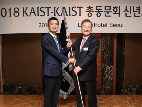 Harnessing the Strength of KAIST Alumni: New Head of KAA Inaugurated
KAIST alumni gathered in Seoul on January 13 to celebrate the New Year and the newly-elected leadership of the KAIST Alumni Association (KAA). More than 300 alumni, including President Sung-Chul Shin who is also an alumnus of KAIST, joined the gala event held at the Lotte Hotel.
Photo: Ki-Chul Cha(left) and Jung Sik Koh(right)
The KAA inaugurated its new president, Ki-Chul Cha, who was preceded by Jung Sik Koh, the former CEO at the Korea Resources Corporation. His term starts from January 2018 to December 2020.
Cha is the CEO of Inbody Co Ltd., a global company specializing in developing and selling medical instruments, such as a body composition analyzers, and medical solutions. He is also an adjunct professor in the Department of Mechanical Engineering at Yonsei University. Cha obtained a master’s degree in Mechanical Engineering at KAIST in 1980, and a Ph.D. in Bioengineering at the University of Utah, before finishing his post-doc fellowship at Harvard Medical School.
Cha plans to explore the idea that alumni engagement, saying, “KAIST stays as a home in the memories of 60,000 alumni. I will dedicate myself to stimulating the alumni association to make KAISTians proud.”
At the gala event, the KAA awarded the Alumni of the Year honor to six alumni who distinguished themselves in the areas of professional achievement, humanitarianism, and public service. They are the Director of Startup KAIST Professor Byoung Yoon Kim; President of LG Chem Ltd and Head of Battery Research and Development Myung Hwan Kim; Director of INNOX Advanced Materials Co., Ltd Kyung Ho Chang; Vice President of the Korea International Trade Association Jung-Kwan Kim; CEO of Samsung Electro-Mechanics Yun-Tae Lee; and CEO of ENF Technology Jinbae Jung.
Photo: President Shin(far right) poses with six awardees of the Distinguished Alumni Award and the former President of KAA, Koh(far left)
2018.01.16 View 10460
 -
 Distinguished Alumni Awards 2017 by KAIST Alumni Association
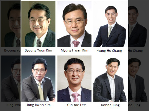
The KAIST Alumni Association announced six Distinguished Alumni Awardees for the year 2017.
Every year, the association selects alumni who have brought honor and distinction to the university through significant contributions to industry, academic achievements, or community service. Since 1992, a total of 95 alumni have been chosen for the distinguished alumni awards.
The recipients are playing major roles in society, and this year is no exception. The award will be given to the alumni during the KAIST New Year Ceremony on January 13 in Seoul.
Here are the six distinguished alumni of the year 2017.
The Director of Startup KAIST, Byoung Yoon Kim (M.S. in Physics) is one of the faculty who has brought entrepreneurship to KAIST. Before founding companies, he held the position of assistant professor at Stanford University. In 1995, he founded FiberProf Inc, commercializing research results from KAIST lab for their applications to test and measurement equipment for lab and production lines. He launched Novera Optics, Inc in 1999 which produced broadband access network equipment (WDM-PON) for FTFH application. Since 2014, he has been holding the position of director of KAIST Startup and inspiring entrepreneurship. He is being recognized for playing a crucial role in defining a successful model for technology startup ecosystems.
The President of LG Chem Ltd., and Head of Battery Research and Development, Myung Hwan Kim (M.S. in Chemical and Biomolecular Engineering) succeeded in developing and producing the first lithium ion batteries in Korea. His work contributed to Korea becoming the second most powerful nation in batteries. In particular, he obtained more orders from global automobile companies by successfully commercializing batteries for electronic vehicles, which led elevating national competitiveness. Recently, his company is leading the battery market for automobiles and power storage by developing novel materials and supplying optimal batteries to match each field.
The Director of INNOX Advanced Materials Co., Ltd., Kyung Ho Chang (M.S. in Chemistry and Ph.D. in Materials Science and Engineering) challenged himself in the Flexible Printed Circuit Board (FPCB) industry, which was mostly dominated by Japanese companies in 2001; however, he succeeded in localizing the materials. Now, his company is the number one for FPCB materials in Korea. FPCBs are a component used in most electronic devices, including smartphones and tablet PCs. Localizing the materials has brought about an import substitution effect as well as establishing a foundation for national competitiveness in FPCBs.
The Vice President of the Korea International Trade Association (KITA), Jung-kwan Kim (M.S. in Business) began his career from deputy director in Ministry of Trade, Industry and Energy. Throughout his career at MOTIE, he served as Director for Energy Development, Director General for Energy Industry Policy, Head Officer of Energy and Resources, and finally Vice Minister for MOTIE. Since joining KITA as the vice president in 2015, he has contributed to supporting overseas expansion of new industries and reinforcing trade competitiveness through opening new markets and providing customized consulting.
The CEO of Samsung Electro-Mechanics, Yun-tae Lee (M.S. and Ph.D. in Electrical Engineering) is an expert in designing semiconductors. While serving as Head of System LSI and Head of LCD in Samsung Electronics, he made significant contributions to projects involving semiconductors and displays, which are the company’s engine of growth. Moreover, by utilizing his insights from the component business and making bold decisions, he is leading the future of Samsung Electro-Mechanics.
The CEO of ENF Technology, Jinbae Jung (Ph.D. in Chemical and Biomolecular Engineering) reinforced national industrial competitiveness by developing high-performance chemicals that are used mostly in the production of semiconductors and displays. Especially, he succeeded in applying regeneration technology of thinners and developing various stripping liquidsHe also localized color pastes, which were heavily dependent on Japan, and improved the quality of color accuracy for LCD panels.
Notable Recipient of Distinguished Alumni Award
2018.01.05 View 8367
 -
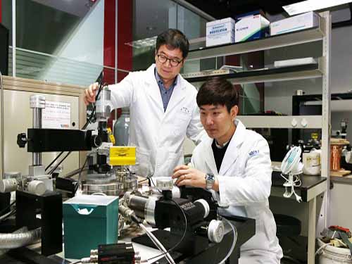 Ultra-Low Power Flexible Memory Using 2D Materials
(Professor Choi and Ph.D. candidate Jang)
KAIST research team led by Professor Sung-Yool Choi at School of Electrical Engineering and Professor Sung Gap Im at the Department of Chemical and Biomolecular Engineering developed high-density, ultra-low power, non-volatile, flexible memory technology using 2D materials. The team used ultrathin molybdenum disulfide (MoS2) with atomic-scale thickness as the channel material and high-performance polymeric insulator film as the tunneling dielectric material. This research was published on the cover of Advanced Functional Materials on November 17. KAIST graduate Myung Hun Woo, a researcher at Samsung Electronics and Ph.D. candidate Byung Chul Jang are first authors.
The surge of new technologies such as Internet of Things (IoT), Artificial Intelligence (AI), and cloud server led to the paradigm shift from processor-centric computing to memory-centric computing in the industry, as well as the increase in demand of wearable devices. This led to an increased need for high-density, ultra-low power, non-volatile flexible memory. In particular, ultrathin MoS2 as semiconductor material has been recently regarded as post-silicon material. This is due to its ultrathin thickness of atomic-scale which suppresses short channel effect observed in conventional silicon material, leading to advantages in high- density and low-power consumption. Further, this thickness allows the material to be flexible, and thus the material is applicable to wearable devices.
However, due to the dangling-bond free surface of MoS2 semiconductor material, it is difficult to deposit the thin insulator film to be uniform and stable over a large area via the conventional atomic layer deposition process. Further, the currently used solution process makes it difficult to deposit uniformly low dielectric constant (k) polymeric insulator film with sub-10 nm thickness on a large area, thus indicating that the memory device utilizing the conventional solution-processed polymer insulator film cannot be operated at low-operating voltage and is not compatible with photolithography.
The research team tried to overcome the hurdles and develop high-density, ultra-low power, non-volatile flexible memory by employing a low-temperature, solvent-free, and all-dry vapor phase technique named initiated chemical vapor deposition (iCVD) process. Using iCVD process, tunneling polymeric insulator film with 10 nm thickness was deposited uniformly on MoS2 semiconductor material without being restricted by the dangling bond-free surface of MoS2. The team observed that the newly developed MoS2-based non-volatile memory can be operated at low-voltage (around 10V), in contrast to the conventional MoS2-based non-volatile memory that requires over 20V.
Professor Choi said, “As the basis for the Fourth Industrial revolution technologies including AI and IoT, semiconductor device technology needs to have characteristics of low-power and flexibility, in clear contrast to conventional memory devices.” He continued, “This new technology is significant in developing source technology in terms of materials, processes, and devices to contribute to achieve these characteristics.”
This research was supported by the Global Frontier Center for Advanced Soft Electronics and the Creative Materials Discovery Program by funded the National Research Foundation of Korea of Ministry of Science and ICT.
( Figure 1. Cover of Advanced Functional Materials)
(Figure 2. Concept map for the developed non-volatile memory material and high-resolution transmission electron microscopy image for material cross-section )
2018.01.02 View 9100
 -
 Non-Adiabatic Reaction Mechanism Identified at Conical Intersection
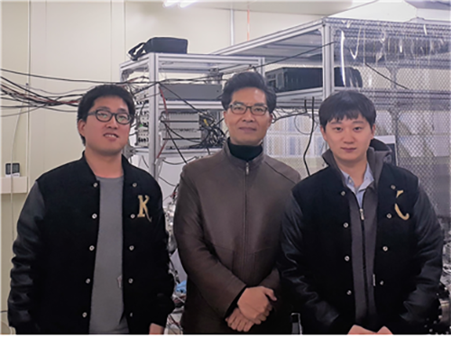
(Professor Kim(center) and Ph.D. candidates Kyung Chul Woo (left) and Kang Do Hyung)
Research team led by Professor Sang Kyu Kim at KAIST Department of Chemistry observed two distinct reaction pathways that occur at conical intersection where two different adiabatic potential energy surfaces cross at the same nuclear configuration.
Professor Kim previously identified the existence and molecular structure of conical intersection in 2010. In this following study, the team accurately measured reaction rates of two totally different reaction pathways activated only at conical intersection where the seminal Born-Oppenheimer approximation breaks down.
This study led by Kyung Chul Woo (1st author) and Do Hyung Kang, both Ph.D. candidates at KAIST, was published in Journal of the American Chemical Society in November 7th, 2017.
Chemical reaction induced by light occurs in excited electronic states where the reaction outcome is often destined by coupling among different electronic states mediated by nuclear motions during chemical reaction. Such a coupling is most critical and important at the conical intersection as nonadiabtic surface-hopping is most probable at situation where the Born-Oppenheimer approximation fails.
Professor Kim used spectroscopic methods in 2010 to experimentally observe conical intersection of polyatomic molecule. And yet, it was not possible to disentangle complex dynamic processes with frequency-domain study only.
The research team used pico-second time-resolution kinetic energy resolved mass spectrometry to identify two possible distinct reaction pathways in both energy and time domains.,.
The research team demonstrated that the reactive flux prepared at the conical intersection is bifurcated into adiabatic or non-adiabatic reaction pathways. These two pathways are quite distinct in terms of reaction rates, energy releases, and product branching ratios.
This is the first study to capture the moment of bifurcation dynamics at the conical intersection for complex polyatomic molecular system. The study could contribute to conceptual improvement in understanding complicated nonadiabatic dynamics in general.
Professor Kim said, “Basic science research is essential in understanding and wisely using the nature. New technological advances cannot be made without the advancement in basic science.” He continued, “I hope this study could lead to growth in many young academic talents in basic sciences.”
(Figure 1. Reaction graph starting from reaction intersection that divides into adiabatic reaction pathway (red) and non-adiabatic pathway (blue))
2017.12.19 View 6226