AT
-
 Highly-Efficient Photoelectrochemical CO2 Reduction
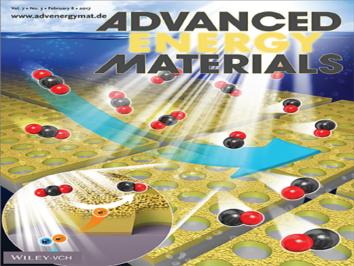
Direct CO2 conversion has continuously attracted a great deal of attention as a technology to produce fuels and chemical building blocks from renewable energy resources. Specifically, substances such as carbon feedstocks and fuels can be produced by utilizing sunlight, water, and CO2 as semiconductors and a water interface through photoelectrochemical CO2 reduction.
A KAIST research team demonstrated a novel photoelectrode structure for highly-selective and efficient photoelectrochemical CO2 reduction reactions. The research team led by Professor Jihun Oh of the Graduate School of EEWS (Energy, Environment, Water and Sustainability) presented a Si photoelectrode with a nanoporous Au thin film that is capable of reducing CO2 to CO with 90 percent selectivity in aqueous solution. The research team’s technology will provide a basic framework for designing the semiconductor photoelectrode structure necessary for photoelectrochemical conversion.
In order to achieve steady conversion of CO2, it is necessary to use a high-performance catalyst to lower overpotential. Among the metal catalysts, Au is known to be an electrocatalyst that converts CO2 to CO.
Conventionally, bare Au, as a catalyst, produces a lot of hydrogen gas due to its low CO selectivity. In addition, the high cost of Au remains a challenge in using the catalyst. Professor Oh’s research team addressed the issue by creating a nanoporous Au thin film formed by the electrochemical reduction of an anodized Au thin film.
As a result, the team could demonstrate an efficient, selective photoelectrochemical reduction reaction of CO2 to CO using electrochemically-treated Au thin films on a Si photoelectrode. The electrochemical reduction on anodized Au thin films forms a nanoporous thin layer exhibiting many grain boundaries of nanoparticles on the Au surface. This dramatically improves the selectivity of the reduction reaction with a maximum CO faradaic efficiency of over 90% at low overpotential and durability.
The research team also used an Au thin film of about 200 nanometers, 50,000 times thinner than previously reported nanostructured Au catalysts, resulting in a cost-effective catalyst. When depositing the catalyst on the semiconductor surface in the type of nanoparticles, the substrate of the thin film will be affected in the course of electrochemical reduction.
Thus, the research team designed a new Si photoelectrode with mesh-type co-catalysts that are independently wired at the front and back of the photoelectrode without influencing the photoelectrode, and made it possible for electrochemical reduction.
Due to the superior CO2 reduction reaction activity of the nanoporous Au mesh and high photovoltage from Si, the Si photoelectrode with the nanoporous Au thin film mesh shows conversion of CO2 to CO with 91% Faradaic efficiency at positive potential than CO equilibrium potential.
Professor Oh explained, “This technology will serve as a platform for diverse semiconductors and catalysts. Researchers can further improve the solar-to-CO2 conversion efficiency using this technology.
Dr. Jun Tae Song, the first author continued, “This new approach made it possible to develop a simple but very important type of electrode structure. It is the first time to achieve CO2 conversion at the potential lower than equilibrium potential. We believe that our research will contribute to efficient CO2 conversion.”
This research was published in the inside front cover of Advanced Energy Materials on February 8, 2017. The research was funded and supported by the Korea Carbon Capture & Sequestration R&D Center. Professor Sung-Yoon Chung of the EEWS also participated in this research.
(Figure: Schematic diagram of a Si photoelectrode that patterns with mesh-type nanoporous Au)
2017.03.08 View 9877
Highly-Efficient Photoelectrochemical CO2 Reduction
Direct CO2 conversion has continuously attracted a great deal of attention as a technology to produce fuels and chemical building blocks from renewable energy resources. Specifically, substances such as carbon feedstocks and fuels can be produced by utilizing sunlight, water, and CO2 as semiconductors and a water interface through photoelectrochemical CO2 reduction.
A KAIST research team demonstrated a novel photoelectrode structure for highly-selective and efficient photoelectrochemical CO2 reduction reactions. The research team led by Professor Jihun Oh of the Graduate School of EEWS (Energy, Environment, Water and Sustainability) presented a Si photoelectrode with a nanoporous Au thin film that is capable of reducing CO2 to CO with 90 percent selectivity in aqueous solution. The research team’s technology will provide a basic framework for designing the semiconductor photoelectrode structure necessary for photoelectrochemical conversion.
In order to achieve steady conversion of CO2, it is necessary to use a high-performance catalyst to lower overpotential. Among the metal catalysts, Au is known to be an electrocatalyst that converts CO2 to CO.
Conventionally, bare Au, as a catalyst, produces a lot of hydrogen gas due to its low CO selectivity. In addition, the high cost of Au remains a challenge in using the catalyst. Professor Oh’s research team addressed the issue by creating a nanoporous Au thin film formed by the electrochemical reduction of an anodized Au thin film.
As a result, the team could demonstrate an efficient, selective photoelectrochemical reduction reaction of CO2 to CO using electrochemically-treated Au thin films on a Si photoelectrode. The electrochemical reduction on anodized Au thin films forms a nanoporous thin layer exhibiting many grain boundaries of nanoparticles on the Au surface. This dramatically improves the selectivity of the reduction reaction with a maximum CO faradaic efficiency of over 90% at low overpotential and durability.
The research team also used an Au thin film of about 200 nanometers, 50,000 times thinner than previously reported nanostructured Au catalysts, resulting in a cost-effective catalyst. When depositing the catalyst on the semiconductor surface in the type of nanoparticles, the substrate of the thin film will be affected in the course of electrochemical reduction.
Thus, the research team designed a new Si photoelectrode with mesh-type co-catalysts that are independently wired at the front and back of the photoelectrode without influencing the photoelectrode, and made it possible for electrochemical reduction.
Due to the superior CO2 reduction reaction activity of the nanoporous Au mesh and high photovoltage from Si, the Si photoelectrode with the nanoporous Au thin film mesh shows conversion of CO2 to CO with 91% Faradaic efficiency at positive potential than CO equilibrium potential.
Professor Oh explained, “This technology will serve as a platform for diverse semiconductors and catalysts. Researchers can further improve the solar-to-CO2 conversion efficiency using this technology.
Dr. Jun Tae Song, the first author continued, “This new approach made it possible to develop a simple but very important type of electrode structure. It is the first time to achieve CO2 conversion at the potential lower than equilibrium potential. We believe that our research will contribute to efficient CO2 conversion.”
This research was published in the inside front cover of Advanced Energy Materials on February 8, 2017. The research was funded and supported by the Korea Carbon Capture & Sequestration R&D Center. Professor Sung-Yoon Chung of the EEWS also participated in this research.
(Figure: Schematic diagram of a Si photoelectrode that patterns with mesh-type nanoporous Au)
2017.03.08 View 9877 -
 13 KAIST Faculty Named as Inaugural Members of Y-KAST
The Korean Academy of Science and Technology (KAST) launched the Young Korean Academy of Science and Technology (Y-KAST) and selected 73 scientists as its inaugural members on February 24. Among them, 13 KAIST faculty were recognized as the inaugural members of Y-KAST.
Y-KAIST, made up of distinguished mid-career scientists under the age of 45, will take the leading role in international collaboration as well as innovative agenda-making in science and technology.
The inaugural members include Professor Hyotcherl Ihee of the Department of Chemistry and Dr. Sung-Jin Oh of the Center for Mathematical Challenges at the Korea Institute for Advanced Study (KIAS), affiliated with KAIST. Professor Ihee is gaining wide acclaim in the fields of physics and chemistry, and in 2016, Dr. Oh was the youngest ever awardee of the Presidential Award of Young Scientist.
The other Y-KAIST members are as follows: Professors Haeshin Lee of the Department of Chemistry; Mi Young Kim, Byung-Kwan Cho, and Ji-Joon Song of the Department of Biological Sciences; Song-Yong Kim of the Department of Mechanical Engineering; Sang-il Oum of the Department of Mathematical Sciences; Jung Kyoon Choi of the Department of Bio and Brain Engineering; Seokwoo Jeon, Sang Ouk Kim, and Il-Doo Kim of the Department of Materials Science and Engineering; Jang Wook Choi of the Graduate School of EEWS (Energy, Environment, Water and Sustainability); and Jeong Ho Lee of the Graduate School of Medical Science and Engineering.
The leading countries of the Academy of Science, which include Germany, Sweden, Belgium, Canada, and Japan, have established the Young Academy of Science since 2010 in order to encourage the research activities of their young scientists and to establish a global platform for collaborative research projects through their active networking at home and abroad.
President Myung-Chul Lee of KAST said, “We will spare no effort to connect these outstanding mid-career researchers for their future collaboration. Their networking will make significant impacts toward their own research activities as well as the global stature of Korea’s science and technology R&D.
(Photo caption: Members of Y-KAST pose at the inaugural ceremony of Y-KAST on February 24.)
2017.03.02 View 17678
13 KAIST Faculty Named as Inaugural Members of Y-KAST
The Korean Academy of Science and Technology (KAST) launched the Young Korean Academy of Science and Technology (Y-KAST) and selected 73 scientists as its inaugural members on February 24. Among them, 13 KAIST faculty were recognized as the inaugural members of Y-KAST.
Y-KAIST, made up of distinguished mid-career scientists under the age of 45, will take the leading role in international collaboration as well as innovative agenda-making in science and technology.
The inaugural members include Professor Hyotcherl Ihee of the Department of Chemistry and Dr. Sung-Jin Oh of the Center for Mathematical Challenges at the Korea Institute for Advanced Study (KIAS), affiliated with KAIST. Professor Ihee is gaining wide acclaim in the fields of physics and chemistry, and in 2016, Dr. Oh was the youngest ever awardee of the Presidential Award of Young Scientist.
The other Y-KAIST members are as follows: Professors Haeshin Lee of the Department of Chemistry; Mi Young Kim, Byung-Kwan Cho, and Ji-Joon Song of the Department of Biological Sciences; Song-Yong Kim of the Department of Mechanical Engineering; Sang-il Oum of the Department of Mathematical Sciences; Jung Kyoon Choi of the Department of Bio and Brain Engineering; Seokwoo Jeon, Sang Ouk Kim, and Il-Doo Kim of the Department of Materials Science and Engineering; Jang Wook Choi of the Graduate School of EEWS (Energy, Environment, Water and Sustainability); and Jeong Ho Lee of the Graduate School of Medical Science and Engineering.
The leading countries of the Academy of Science, which include Germany, Sweden, Belgium, Canada, and Japan, have established the Young Academy of Science since 2010 in order to encourage the research activities of their young scientists and to establish a global platform for collaborative research projects through their active networking at home and abroad.
President Myung-Chul Lee of KAST said, “We will spare no effort to connect these outstanding mid-career researchers for their future collaboration. Their networking will make significant impacts toward their own research activities as well as the global stature of Korea’s science and technology R&D.
(Photo caption: Members of Y-KAST pose at the inaugural ceremony of Y-KAST on February 24.)
2017.03.02 View 17678 -
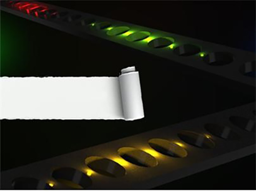 Semiconductor Photonic Nanocavities on Paper Substrates
Professor Yong-Hoon Cho of the Department of Physics and his team at KAIST have developed a semiconductor photonic nanocavity laser that can operate on a paper substrate.
The researchers hope that this novel method, which involves transferring nano-sized photonic crystal particles onto a paper substrate with high absorptiveness, will enable the diagnoses of various diseases by using high-tech semiconductor sensors at low cost.
The results of this research were published in the November 17th, 2016, issue of Advanced Materials.
Photonic crystals, which utilize light as a medium to provide high bandwidths, can transfer large amounts of information. Compared with their electronic counterparts, photonic crystals also consume less energy to operate.
Normally, semiconductor photonic particles require substrates, which play only a passive role in the assembly and endurance of individual, functional photonic components. These substrates, however, are bulky and environmentally hazardous as they are made up of non-biodegradable materials.
The research team overcame these two shortcomings by replacing a semiconductor substrate with standard paper. The substrate’s mass was reduced considerably, and because paper is made from trees, it degrades. Paper can be easily and cheaply acquired from our surroundings, which drastically reduces the unit cost of semiconductors.
In addition, paper possesses superior mechanical characteristics. It is flexible and can be repeatedly folded and unfolded without being torn. These are traits that have long been sought by researchers for existing flexible substrates.
The research team used a micro-sized stamp to detach photonic crystal nanobeam cavities selectively from their original substrate and transfer them onto a new paper substrate. Using this technique, the team removed nanophotonic crystals that had been patterned (using a process of selectively etching circuits onto a substrate) onto a semiconductor substrate with a high degree of integration, and realigned them as desired on a paper substrate.
The nanophotonic crystals that the team combined with paper in this research were 0.5 micrometers in width, 6 micrometers in length, and 0.3 micrometers in height—about one-hundredth of the width of a single hair (0.1 millimeter).
The team also transferred their photonic crystals onto paper with a fluid channel, which proved that it could be used as a refractive index sensor. As can be seen in current commercial pregnancy diagnosis kits, paper has high absorptiveness. Since photonic crystal particles have high sensitivity, they are highly suitable for applications such as sensors.
Professor Cho stated that “by using paper substrates, this technology can greatly contribute to the rising field of producing environmentally-friendly photonic particles” and “by combining inexpensive paper and high-performance photonic crystal sensors, we can obtain low prices as well as designing appropriate technologies with high performance.”
Dr. Sejeong Kim of the Department of Physics participated in this study as the first author, and Professor Kwanwoo Shin of Sogang University and Professor Yong-Hee Lee of KAIST also took part in this research. The research was supported by the National Research Foundation’s Mid-Career Researcher Program, and the Climate Change Research Hub of KAIST.
Figure 1. Illustration of photonic crystal lasers on paper substrates
Figure 2. Photonic crystal resonator laser and refractive index sensor operating on paper substrates
2017.03.01 View 7593
Semiconductor Photonic Nanocavities on Paper Substrates
Professor Yong-Hoon Cho of the Department of Physics and his team at KAIST have developed a semiconductor photonic nanocavity laser that can operate on a paper substrate.
The researchers hope that this novel method, which involves transferring nano-sized photonic crystal particles onto a paper substrate with high absorptiveness, will enable the diagnoses of various diseases by using high-tech semiconductor sensors at low cost.
The results of this research were published in the November 17th, 2016, issue of Advanced Materials.
Photonic crystals, which utilize light as a medium to provide high bandwidths, can transfer large amounts of information. Compared with their electronic counterparts, photonic crystals also consume less energy to operate.
Normally, semiconductor photonic particles require substrates, which play only a passive role in the assembly and endurance of individual, functional photonic components. These substrates, however, are bulky and environmentally hazardous as they are made up of non-biodegradable materials.
The research team overcame these two shortcomings by replacing a semiconductor substrate with standard paper. The substrate’s mass was reduced considerably, and because paper is made from trees, it degrades. Paper can be easily and cheaply acquired from our surroundings, which drastically reduces the unit cost of semiconductors.
In addition, paper possesses superior mechanical characteristics. It is flexible and can be repeatedly folded and unfolded without being torn. These are traits that have long been sought by researchers for existing flexible substrates.
The research team used a micro-sized stamp to detach photonic crystal nanobeam cavities selectively from their original substrate and transfer them onto a new paper substrate. Using this technique, the team removed nanophotonic crystals that had been patterned (using a process of selectively etching circuits onto a substrate) onto a semiconductor substrate with a high degree of integration, and realigned them as desired on a paper substrate.
The nanophotonic crystals that the team combined with paper in this research were 0.5 micrometers in width, 6 micrometers in length, and 0.3 micrometers in height—about one-hundredth of the width of a single hair (0.1 millimeter).
The team also transferred their photonic crystals onto paper with a fluid channel, which proved that it could be used as a refractive index sensor. As can be seen in current commercial pregnancy diagnosis kits, paper has high absorptiveness. Since photonic crystal particles have high sensitivity, they are highly suitable for applications such as sensors.
Professor Cho stated that “by using paper substrates, this technology can greatly contribute to the rising field of producing environmentally-friendly photonic particles” and “by combining inexpensive paper and high-performance photonic crystal sensors, we can obtain low prices as well as designing appropriate technologies with high performance.”
Dr. Sejeong Kim of the Department of Physics participated in this study as the first author, and Professor Kwanwoo Shin of Sogang University and Professor Yong-Hee Lee of KAIST also took part in this research. The research was supported by the National Research Foundation’s Mid-Career Researcher Program, and the Climate Change Research Hub of KAIST.
Figure 1. Illustration of photonic crystal lasers on paper substrates
Figure 2. Photonic crystal resonator laser and refractive index sensor operating on paper substrates
2017.03.01 View 7593 -
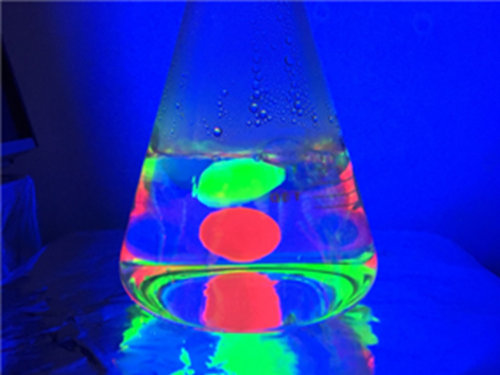 Quantum Dot Film Can Withstand High Temperatures and Humidity
The joint KAIST research team of Professor Byeong-Soo Bae of the Department of Materials Science and Engineering and Professor Doh Chang Lee of the Department of Chemical and Biomolecular Engineering was able to fabricate a siloxane-encapsulated quantum dot film, which exhibits stable emission intensity over one month even at high temperatures and humidity.
The results of this study were published in the Journal of the American Chemical Society (JACS) on November 29, 2016. The research article is entitled “Quantum Dot/Siloxane Composite Film Exceptionally Stable against Oxidation under Heat and Moisture.” (DOI: 10.1021/jacs.6b10681)
Quantum dots (QDs), light-emitting diodes (LEDs) for next-generation displays, are tiny particles or nanocrystals of semiconducting materials. Their emission wavelength can easily be adjusted by changing their sizes, which are just a few nanometers. A wide spectrum of their colors can also achieve ultra-high definition displays.
Due to these characteristics, QDs are coated on a film as a polymer resin in dispersed form, or they are spread on an LED light source. They are thus considered to be crucial for next generation displays.
Despite their exceptional optical properties, however, QDs are easily oxidized in a high temperature and high humidity environment, and, as a result, this greatly deteriorates their luminescence quality (quantum efficiency). Therefore, they are encapsulated in an extra thin layer to block oxygen and moisture.
QD displays in the current market have a film inserted to separate them from LEDs, which create heat. The high unit cost of this protective layer, however, increases the overall cost of displays, lowering their price competitiveness in the market.
For a solution, the research team applied the sol-gel condensation reaction of silane precursors with QDs. This technology uses the reactions of chemical substances to synthesize ceramics or glass at a low temperature.
The team applied QDs in a heat resistant siloxane polymer by employing this technology. The siloxane resin acted as a cup holding the QDs and also blocked heat and moisture. Thus, their performance can be maintained without an extra protective film.
QDs are evenly dispersed into the resin from a chemical process to fabricate a QD embedded film and retained the high quality luminescence not only at a high temperature of 85°C and in a high humidity of 85%, but also in a high acid and high base environment. Remarkably though, the luminescence actually increased in the high humidity environment.
If this technology is used, the overall price of displays will decrease by producing a stable QD film without an extra protective barrier. In the future, the QD film can be directly applied to a blue LED light source. As a result, it will be possible to develop a QD display that can reduce the amount of QDs needed and improve its performance.
Professor Bae said, “We have proposed a way to make quantum dots overcome their limitations and have wide applications as they are being developed for next-generation displays. Our technology will make significant contributions to the display industry in the country.”
He also added, “In the future, we plan to cooperate with companies both in and out of the country to improve the performance of quantum dots and concentrate on their commercialization.”
The research team is currently applying for related patents both in and out of the country. The team is also plan ning to transfer the patents to Sol Ip Technology Inc., a company founded at KAIST, to start the commercialization.
Picture 1:
Siloxane-encapsulated quantum dot (QD) films showing performance stability in boiling water
Picture 2 and 3:
So-gel condensation reaction in silane precursors between Methacryloxypropyltrimethoxysilane (MPTS) and diphenylsilanediol (DPSD). The inset shows photographs of a QD-oligosiloxane resin under room light (left) and a UV lamp (λ = 365 nm) (right).
Free radical addition reactions among carbon double bonds of methacryl functional groups and oleic acids. The inset shows photographs of a QD-silox film under room light (left) and a UV lamp (λ = 365 nm) (right).
2017.02.24 View 10348
Quantum Dot Film Can Withstand High Temperatures and Humidity
The joint KAIST research team of Professor Byeong-Soo Bae of the Department of Materials Science and Engineering and Professor Doh Chang Lee of the Department of Chemical and Biomolecular Engineering was able to fabricate a siloxane-encapsulated quantum dot film, which exhibits stable emission intensity over one month even at high temperatures and humidity.
The results of this study were published in the Journal of the American Chemical Society (JACS) on November 29, 2016. The research article is entitled “Quantum Dot/Siloxane Composite Film Exceptionally Stable against Oxidation under Heat and Moisture.” (DOI: 10.1021/jacs.6b10681)
Quantum dots (QDs), light-emitting diodes (LEDs) for next-generation displays, are tiny particles or nanocrystals of semiconducting materials. Their emission wavelength can easily be adjusted by changing their sizes, which are just a few nanometers. A wide spectrum of their colors can also achieve ultra-high definition displays.
Due to these characteristics, QDs are coated on a film as a polymer resin in dispersed form, or they are spread on an LED light source. They are thus considered to be crucial for next generation displays.
Despite their exceptional optical properties, however, QDs are easily oxidized in a high temperature and high humidity environment, and, as a result, this greatly deteriorates their luminescence quality (quantum efficiency). Therefore, they are encapsulated in an extra thin layer to block oxygen and moisture.
QD displays in the current market have a film inserted to separate them from LEDs, which create heat. The high unit cost of this protective layer, however, increases the overall cost of displays, lowering their price competitiveness in the market.
For a solution, the research team applied the sol-gel condensation reaction of silane precursors with QDs. This technology uses the reactions of chemical substances to synthesize ceramics or glass at a low temperature.
The team applied QDs in a heat resistant siloxane polymer by employing this technology. The siloxane resin acted as a cup holding the QDs and also blocked heat and moisture. Thus, their performance can be maintained without an extra protective film.
QDs are evenly dispersed into the resin from a chemical process to fabricate a QD embedded film and retained the high quality luminescence not only at a high temperature of 85°C and in a high humidity of 85%, but also in a high acid and high base environment. Remarkably though, the luminescence actually increased in the high humidity environment.
If this technology is used, the overall price of displays will decrease by producing a stable QD film without an extra protective barrier. In the future, the QD film can be directly applied to a blue LED light source. As a result, it will be possible to develop a QD display that can reduce the amount of QDs needed and improve its performance.
Professor Bae said, “We have proposed a way to make quantum dots overcome their limitations and have wide applications as they are being developed for next-generation displays. Our technology will make significant contributions to the display industry in the country.”
He also added, “In the future, we plan to cooperate with companies both in and out of the country to improve the performance of quantum dots and concentrate on their commercialization.”
The research team is currently applying for related patents both in and out of the country. The team is also plan ning to transfer the patents to Sol Ip Technology Inc., a company founded at KAIST, to start the commercialization.
Picture 1:
Siloxane-encapsulated quantum dot (QD) films showing performance stability in boiling water
Picture 2 and 3:
So-gel condensation reaction in silane precursors between Methacryloxypropyltrimethoxysilane (MPTS) and diphenylsilanediol (DPSD). The inset shows photographs of a QD-oligosiloxane resin under room light (left) and a UV lamp (λ = 365 nm) (right).
Free radical addition reactions among carbon double bonds of methacryl functional groups and oleic acids. The inset shows photographs of a QD-silox film under room light (left) and a UV lamp (λ = 365 nm) (right).
2017.02.24 View 10348 -
 Prof. Woo Chang Kim Is Appointed as Managing Editor of Quantitative Finance
Professor Woo Chang Kim of the Industrial and Systems Engineering Department has been elected as the Managing Editor of Quantitative Finance.
Founded in 2001, Quantitative Finance has been an internationally-acclaimed peer-reviewed journal in the field of financial engineering, along with Mathematical Finance.
This is the first time for a Korean researcher to be named for the editorial board, which consists of eminent scholars from around the world, including four Nobel laureates.
Professor Kim’s expertise lies in financial optimization, portfolio management, and asset liability management. In recent years, he has focused his research on robo-advisors in the area of FinTech, and for this contribution, he was appointed as managing editor.
Professor Kim also served as an editor, deputy editor, and a member of the editorial boards for various journals, including the Journal of Portfolio Management and Optimization and Engineering. Currently, he serves as a member of the Korean National Pension Fund’s Electoral Commission, an adviser to Samsung Asset Management Co., Ltd., and the director of the KAIST Asset Management for Future Technology Research Center that was opened in October 2016.
2017.02.23 View 8227
Prof. Woo Chang Kim Is Appointed as Managing Editor of Quantitative Finance
Professor Woo Chang Kim of the Industrial and Systems Engineering Department has been elected as the Managing Editor of Quantitative Finance.
Founded in 2001, Quantitative Finance has been an internationally-acclaimed peer-reviewed journal in the field of financial engineering, along with Mathematical Finance.
This is the first time for a Korean researcher to be named for the editorial board, which consists of eminent scholars from around the world, including four Nobel laureates.
Professor Kim’s expertise lies in financial optimization, portfolio management, and asset liability management. In recent years, he has focused his research on robo-advisors in the area of FinTech, and for this contribution, he was appointed as managing editor.
Professor Kim also served as an editor, deputy editor, and a member of the editorial boards for various journals, including the Journal of Portfolio Management and Optimization and Engineering. Currently, he serves as a member of the Korean National Pension Fund’s Electoral Commission, an adviser to Samsung Asset Management Co., Ltd., and the director of the KAIST Asset Management for Future Technology Research Center that was opened in October 2016.
2017.02.23 View 8227 -
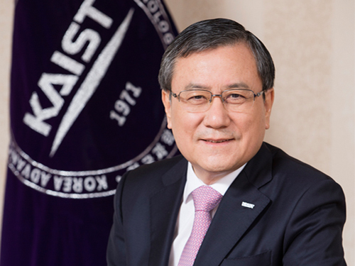 Dr. Sung-Chul Shin Selected 16th President of KAIST
(President Sung-Chul Shin)
The KAIST Board of Trustees elected Professor Sung-Chul Shin of the Department of Physics the 16th president of KAIST on February 21. Professor Shin succeeds President Sung-Mo Kang whose four-year term will end on February 23. He is the first KAIST alumnus to serve as its president.
The Board of Trustees announced, “We believe that Professor Shin’s scientific achievement, outstanding leadership, and clear vision will serve KAIST faculty, students, and staff very well. He will be the best person to help KAIST leap forward in the four years ahead.”
The newly-elected president said, “I am humbled and honored to have been elected to lead such a prestigious institute of Korea. Aiming to be one of the top ten global universities, KAIST will continue to innovate its systems.” Previously, Dr. Shin led the Daegu Gyeongbuk Institute of Science and Technology (DGIST) for six years as president since 2011.
Professor Shin joined the KAIST faculty in 1989. He graduated from Seoul National University and then earned his MS degree in condensed matter physics at KAIST in 1977. After earning his Ph.D. in material physics at Northwestern University in 1984, he worked at Eastman Kodak Research Labs as a senior research scientist for five years.
Before heading to DGIST, President Shin held key administrative positions at KAIST from the early 1990s including dean of planning, dean of the international office, and vice-dean of student affairs. During President Robert Laughlin’s tenure, the first foreign president at KAIST, he served as vice-president for two years from 2004. He also served on the Presidential Advisory Council on Science and Technology of the Korean government as vice chairperson from 2015 to 2016.
A renowned scholar in the field of nanoscience, President Shin’s research focuses on the artificial synthesis and characterization of nonmagnetic materials, magnetic anisotropy, and magneto-optical phenomena. He leads the Laboratory for Nanospinics of Spintronic Materials at KAIST and has published in 290 journals while holding 37 patents.
A fellow in the American Physical Society (APS) since 2008, he was the president of the Korean Physical Society from 2011 to 2012. He has been on the editorial board of J. Magnetism and Magnetic Materials from 2009 and was the first Korean recipient of the Asian Union of Magnetics Societies (AUMS) Award, which recognizes outstanding scientists in the field of magnetics.
President Shin envisions making KAIST’s research and education more competitive through continuing innovation. His innovation efforts will extend to the five key areas of education, research, technology commercialization, globalization, and future planning.
Among his priorities, he emphasizes multidisciplinary studies and leadership training for students. He plans to focus on undeclared major courses for undergraduates to help them expand their experience and exposure to diverse disciplines. This approach will help create well-rounded engineers, scientists, and entrepreneurs by enabling them to develop skills while leveraging a strong connection to the arts, humanities, and social sciences.
To better respond to Industry 4.0, which calls for convergence studies and collaborative work, he proposed establishing a ‘Convergence Innovation System’ by strategically selecting 10 flagship convergence research groups. In order to accelerate the technology commercialization and ecosystem of start-ups, he will strengthen entrepreneurship education, making it a prerequisite requirement for students. President Shin said he will spare no effort to incubate and spin-off ventures in which KAIST technology is being transferred. For globalization efforts, he plans to increase the ratio of foreign faculty from 9 percent to 15 percent, while doubling the current foreign student enrollment ratio of 5 percent. For future strategic innovation, he will implement a long-term innovation strategic plan dubbed ‘Vision 2031.’
2017.02.22 View 11238
Dr. Sung-Chul Shin Selected 16th President of KAIST
(President Sung-Chul Shin)
The KAIST Board of Trustees elected Professor Sung-Chul Shin of the Department of Physics the 16th president of KAIST on February 21. Professor Shin succeeds President Sung-Mo Kang whose four-year term will end on February 23. He is the first KAIST alumnus to serve as its president.
The Board of Trustees announced, “We believe that Professor Shin’s scientific achievement, outstanding leadership, and clear vision will serve KAIST faculty, students, and staff very well. He will be the best person to help KAIST leap forward in the four years ahead.”
The newly-elected president said, “I am humbled and honored to have been elected to lead such a prestigious institute of Korea. Aiming to be one of the top ten global universities, KAIST will continue to innovate its systems.” Previously, Dr. Shin led the Daegu Gyeongbuk Institute of Science and Technology (DGIST) for six years as president since 2011.
Professor Shin joined the KAIST faculty in 1989. He graduated from Seoul National University and then earned his MS degree in condensed matter physics at KAIST in 1977. After earning his Ph.D. in material physics at Northwestern University in 1984, he worked at Eastman Kodak Research Labs as a senior research scientist for five years.
Before heading to DGIST, President Shin held key administrative positions at KAIST from the early 1990s including dean of planning, dean of the international office, and vice-dean of student affairs. During President Robert Laughlin’s tenure, the first foreign president at KAIST, he served as vice-president for two years from 2004. He also served on the Presidential Advisory Council on Science and Technology of the Korean government as vice chairperson from 2015 to 2016.
A renowned scholar in the field of nanoscience, President Shin’s research focuses on the artificial synthesis and characterization of nonmagnetic materials, magnetic anisotropy, and magneto-optical phenomena. He leads the Laboratory for Nanospinics of Spintronic Materials at KAIST and has published in 290 journals while holding 37 patents.
A fellow in the American Physical Society (APS) since 2008, he was the president of the Korean Physical Society from 2011 to 2012. He has been on the editorial board of J. Magnetism and Magnetic Materials from 2009 and was the first Korean recipient of the Asian Union of Magnetics Societies (AUMS) Award, which recognizes outstanding scientists in the field of magnetics.
President Shin envisions making KAIST’s research and education more competitive through continuing innovation. His innovation efforts will extend to the five key areas of education, research, technology commercialization, globalization, and future planning.
Among his priorities, he emphasizes multidisciplinary studies and leadership training for students. He plans to focus on undeclared major courses for undergraduates to help them expand their experience and exposure to diverse disciplines. This approach will help create well-rounded engineers, scientists, and entrepreneurs by enabling them to develop skills while leveraging a strong connection to the arts, humanities, and social sciences.
To better respond to Industry 4.0, which calls for convergence studies and collaborative work, he proposed establishing a ‘Convergence Innovation System’ by strategically selecting 10 flagship convergence research groups. In order to accelerate the technology commercialization and ecosystem of start-ups, he will strengthen entrepreneurship education, making it a prerequisite requirement for students. President Shin said he will spare no effort to incubate and spin-off ventures in which KAIST technology is being transferred. For globalization efforts, he plans to increase the ratio of foreign faculty from 9 percent to 15 percent, while doubling the current foreign student enrollment ratio of 5 percent. For future strategic innovation, he will implement a long-term innovation strategic plan dubbed ‘Vision 2031.’
2017.02.22 View 11238 -
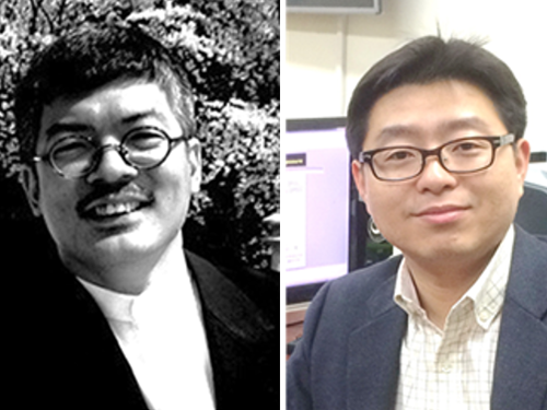 Professor Shin Honored Posthumously for Iridescent Microparticles
(The Late Professor Joong-Hoon Shin (left) and Professor Shin-Hyun Kim)
A research team co-led by Professor Shin-Hyun Kim from the Department of Chemical and Biomolecular Engineering and Professor Jong-Ryul Jeong from the Department of Materials Science and Engineering at Chungnam National University developed iridescent microparticles with a structural color gradient. The research team posthumously dedicated their research to a renowned professor in the field of nanophotonics, the late Professor Joong-Hoon Shin of the Graduate School of Nanoscience and Technology at KAIST. He passed away suddenly in a car accident last September.
The iridescent microparticles, which allow on-demand control over structural color, will be key components for next-generation reflection-mode displays with clear color realization even in direct sunlight.
Materials such as opals, Morpho butterfly wings, and peacock feathers all display beautiful colors without pigment, using regularly-spaced nanostructures. Regularly-spaced nanostructures render color, by selectively reflecting the light of a particular wave through light interference. As such, materials that possess periodic modulation of refractive index at subwavelength scale are referred to as photonic crystals.
In general, photonic crystals are only able to display a single color, so limitations exist when attempting to apply them to reflection-mode displays which call for multiple structural colors. The research team addressed the issue using inspiration from snowflakes stacking in the winter. When snow falls on the surface of a round-shaped structure, the thickness of the snow stacking differs depending on the orientation. Based on this observation, the research team created photonic microparticles with a structural color gradient by depositing two different materials on spherical microparticles.
When some material is deposited on the surface of a sphere, the material on the top is thickest and becomes thinner on the sides. The team alternately deposited titania and silica on the spherical microparticles to form periodic modulation of the refractive index. The thickness of the alternating photonic layers is reduced along the angle from the top, which yields a structural color gradient.
Consequently, the microparticles reflect long-wavelength red light from the top of the sphere and short-wavelength blue light from the side of the sphere. Any color of the visible spectrum can be selected in between the top and side depending on the orientation of the microparticles.
The research team used an external magnetic field as a way to control the orientation of the photonic microparticles and the structural colors. As magnetic iron layer was deposited underneath the alternating photonic layer, it was possible to freely control the orientation of the microparticles using a magnet, thereby allowing control of the color seen by the users.
KAIST doctoral candidate Seung Yeol Lee of the Department of Chemical and Biomolecular Engineering is the first author of this research, with support from the Midcareer Researcher Program of the National Research Foundation and funded by the Ministry of Science, ICT, and Future Planning (MSIP). This research was published in the online edition of Advanced Materials on February 6, 2017.
Figure1: Sets of an OM image of photonic Janus microspheres and an SEM image showing a cross-section of the photonic layers.
Figure 2: A series of schematics and OM images showing the color change depending on the orientation angle of the photonic Janus microsphere.
2017.02.17 View 8811
Professor Shin Honored Posthumously for Iridescent Microparticles
(The Late Professor Joong-Hoon Shin (left) and Professor Shin-Hyun Kim)
A research team co-led by Professor Shin-Hyun Kim from the Department of Chemical and Biomolecular Engineering and Professor Jong-Ryul Jeong from the Department of Materials Science and Engineering at Chungnam National University developed iridescent microparticles with a structural color gradient. The research team posthumously dedicated their research to a renowned professor in the field of nanophotonics, the late Professor Joong-Hoon Shin of the Graduate School of Nanoscience and Technology at KAIST. He passed away suddenly in a car accident last September.
The iridescent microparticles, which allow on-demand control over structural color, will be key components for next-generation reflection-mode displays with clear color realization even in direct sunlight.
Materials such as opals, Morpho butterfly wings, and peacock feathers all display beautiful colors without pigment, using regularly-spaced nanostructures. Regularly-spaced nanostructures render color, by selectively reflecting the light of a particular wave through light interference. As such, materials that possess periodic modulation of refractive index at subwavelength scale are referred to as photonic crystals.
In general, photonic crystals are only able to display a single color, so limitations exist when attempting to apply them to reflection-mode displays which call for multiple structural colors. The research team addressed the issue using inspiration from snowflakes stacking in the winter. When snow falls on the surface of a round-shaped structure, the thickness of the snow stacking differs depending on the orientation. Based on this observation, the research team created photonic microparticles with a structural color gradient by depositing two different materials on spherical microparticles.
When some material is deposited on the surface of a sphere, the material on the top is thickest and becomes thinner on the sides. The team alternately deposited titania and silica on the spherical microparticles to form periodic modulation of the refractive index. The thickness of the alternating photonic layers is reduced along the angle from the top, which yields a structural color gradient.
Consequently, the microparticles reflect long-wavelength red light from the top of the sphere and short-wavelength blue light from the side of the sphere. Any color of the visible spectrum can be selected in between the top and side depending on the orientation of the microparticles.
The research team used an external magnetic field as a way to control the orientation of the photonic microparticles and the structural colors. As magnetic iron layer was deposited underneath the alternating photonic layer, it was possible to freely control the orientation of the microparticles using a magnet, thereby allowing control of the color seen by the users.
KAIST doctoral candidate Seung Yeol Lee of the Department of Chemical and Biomolecular Engineering is the first author of this research, with support from the Midcareer Researcher Program of the National Research Foundation and funded by the Ministry of Science, ICT, and Future Planning (MSIP). This research was published in the online edition of Advanced Materials on February 6, 2017.
Figure1: Sets of an OM image of photonic Janus microspheres and an SEM image showing a cross-section of the photonic layers.
Figure 2: A series of schematics and OM images showing the color change depending on the orientation angle of the photonic Janus microsphere.
2017.02.17 View 8811 -
 An Improved Carbon Nanotube Semiconductor
Professor Yang-Kyu Choi and his research team of the School of Electrical Engineering at KAIST collaborated with Professor Sung-Jin Choi of Kookmin University to develop a large-scale carbon nanotube semiconductor by using a 3-D fin-gate structure with carbon nanotubes on its top.
Dong Il Lee, a postdoctoral researcher at KAIST’s Electrical Engineering School, participated in this study as the first author. It was published in ACS Nano on November 10, 2016, and was entitled “Three-Dimensional Fin-Structured Semiconducting Carbon Nanotube Network Transistor.”
A semiconductor made with carbon nanotubes operates faster than a silicon semiconductor and requires less energy, yielding higher performance.
Most electronic equipment and devices, however, use silicon semiconductors because it is difficult to fabricate highly purified and densely packed semiconductors with carbon nanotubes (CNTs).
To date, the performance of CNTs was limited due to their low density. Their purity was also low, so it was impossible to make products that had a constant yield on a large-surface wafer or substrate. These characteristics made the mass production of semiconducting CNTs difficult.
To solve these difficulties, the research team used a 3-D fin-gate to vapor-deposit carbon nanotubes on its top. They developed a semiconductor that had a high current density with a width less than 50 nm.
The three-dimensional fin structure was able to vapor-deposit 600 carbon nanotubes per micrometer. This structure could have 20 times more nanotubes than the two dimensional structure, which could only vapor-deposit thirty in the same 1 micrometer width.
In addition, the research team used semi-conductive carbon nanotubes having a purity rating higher than 99.9% from a previous study to obtain a high yield semiconductor.
The semiconductor from the research group has a high current density even with a width less than 50 μm. The new semiconductor is expected to be five times faster than a silicon-based semiconductor and will require five times less electricity during operation.
Furthermore, the new semiconductor can be made by or will be compatible with the equipment for producing silicon-based semiconductors, so there will be no additional costs.
Researcher Lee said, “As a next generation semiconductor, the carbon nanotube semiconductor will have better performance, and its effectiveness will be higher.” He also added, “Hopefully, the new semiconductor will replace the silicon-based semiconductors in ten years.”
This study received support from the Center for Integrated Smart Sensors funded by the Ministry of Science, ICT & Future Planning of Korea as the Global Frontier Project, and from the CMOS (Complementary Metal-Oxide-Semiconductor) THz Technology Convergence Center of the Pioneer Research Center Program sponsored by the National Research Foundation of Korea.
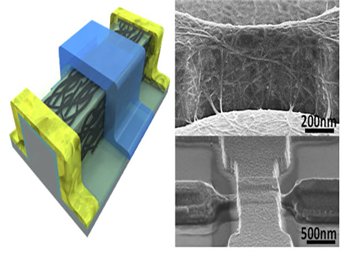
Picture 1: 3D Diagram of the Carbon Nanotube Electronic Device and Its Scanning Electron Microscope (SEM) Image
Picture 2: 3D Transistor Device on an 8-inch Base and the SEM Image of Its Cross Section
2017.02.16 View 10939
An Improved Carbon Nanotube Semiconductor
Professor Yang-Kyu Choi and his research team of the School of Electrical Engineering at KAIST collaborated with Professor Sung-Jin Choi of Kookmin University to develop a large-scale carbon nanotube semiconductor by using a 3-D fin-gate structure with carbon nanotubes on its top.
Dong Il Lee, a postdoctoral researcher at KAIST’s Electrical Engineering School, participated in this study as the first author. It was published in ACS Nano on November 10, 2016, and was entitled “Three-Dimensional Fin-Structured Semiconducting Carbon Nanotube Network Transistor.”
A semiconductor made with carbon nanotubes operates faster than a silicon semiconductor and requires less energy, yielding higher performance.
Most electronic equipment and devices, however, use silicon semiconductors because it is difficult to fabricate highly purified and densely packed semiconductors with carbon nanotubes (CNTs).
To date, the performance of CNTs was limited due to their low density. Their purity was also low, so it was impossible to make products that had a constant yield on a large-surface wafer or substrate. These characteristics made the mass production of semiconducting CNTs difficult.
To solve these difficulties, the research team used a 3-D fin-gate to vapor-deposit carbon nanotubes on its top. They developed a semiconductor that had a high current density with a width less than 50 nm.
The three-dimensional fin structure was able to vapor-deposit 600 carbon nanotubes per micrometer. This structure could have 20 times more nanotubes than the two dimensional structure, which could only vapor-deposit thirty in the same 1 micrometer width.
In addition, the research team used semi-conductive carbon nanotubes having a purity rating higher than 99.9% from a previous study to obtain a high yield semiconductor.
The semiconductor from the research group has a high current density even with a width less than 50 μm. The new semiconductor is expected to be five times faster than a silicon-based semiconductor and will require five times less electricity during operation.
Furthermore, the new semiconductor can be made by or will be compatible with the equipment for producing silicon-based semiconductors, so there will be no additional costs.
Researcher Lee said, “As a next generation semiconductor, the carbon nanotube semiconductor will have better performance, and its effectiveness will be higher.” He also added, “Hopefully, the new semiconductor will replace the silicon-based semiconductors in ten years.”
This study received support from the Center for Integrated Smart Sensors funded by the Ministry of Science, ICT & Future Planning of Korea as the Global Frontier Project, and from the CMOS (Complementary Metal-Oxide-Semiconductor) THz Technology Convergence Center of the Pioneer Research Center Program sponsored by the National Research Foundation of Korea.
Picture 1: 3D Diagram of the Carbon Nanotube Electronic Device and Its Scanning Electron Microscope (SEM) Image
Picture 2: 3D Transistor Device on an 8-inch Base and the SEM Image of Its Cross Section
2017.02.16 View 10939 -
 A New Approach to 3D Holographic Displays Greatly Improves the Image Quality
With the addition of holographic diffusers or frosted glasses to wavefront modulators, KAIST researchers offer a simple and practical solution to significantly enhance the performance of 3D dynamic holographic displays by 2,600 times.
The potential applications of three-dimensional (3D) digital holograms are enormous. In addition to arts and entertainment, various fields including biomedical imaging, scientific visualization, engineering design, and displays could benefit from this technology. For example, creating full-sized organs for 3D analysis by doctors could be helpful, but it remained a challenge owing to the limitation of hologram-generation techniques.
A research team led by Professor YongKeun Park of the Physics Department at KAIST has come up with a solution and developed a 3D holographic display that performs more than 2,600 times better than existing 3D holographic displays. This study is expected to improve the limited size and viewing angle of 3D images, which were a major problem of the current holographic displays. The study was published online in Nature Photonics on January 23, 2017.
3D holograms, which often appear in science fiction films, are a familiar technology to the public, but holograms in movies are created with computer graphic effects. Methods for creating true 3D holograms are still being studied in the laboratory. For example, due to the difficulty of generating real 3D images, recent virtual reality (VR) and augmented reality (AR) devices project two different two-dimensional (2D) images onto a viewer to induce optical illusions.
To create a 3D hologram that can be viewed without special equipment such as 3D glasses, the wavefront of light must be controlled using wavefront modulators such as spatial light modulators (SLMs) and deformable mirrors (DMs). A wavefront modulator is an optical manipulation device that can control the direction of light propagation.
However, the biggest limitation to using these modulators as 3D displays is the number of pixels. The large number of pixels that are packed into high-resolution displays developed in recent years are suitable for a 2D image, and the amount of information contained in those pixels cannot produce a 3D image. For this reason, a 3D image that can be made with existing wavefront modulator technology is 1 cm in size with a narrow viewing angle of 3 degrees, which is far from practicable.
As an alternative, KAIST researchers used a DM and added two successive holographic diffusers to scatter light. By scattering light in many directions, this allows for a wider viewing angle and larger image, but results in volume speckle fields, which are caused by the interference of multiple scattered light. Random volume speckle fields cannot be used to display 3D images.
To fix the problem, the researchers employed a wavefront-shaping technique to control the fields. As a result, they succeeded in producing an enhanced 3D holographic image with a viewing angle of 35 degrees in a volume of 2 cm in length, width, and height. This yielded a performance that was about 2,600 times stronger than the original image definition generated when they used a DM without a diffuser.
Professor Park said, “Scattering light has previously been believed to interfere with the recognition of objects, but we have demonstrated that current 3D displays can be improved significantly with an increased viewing angle and image size by properly controlling the scattered light.”
Hyeonseung Yu, who is the lead author of this research article and a doctoral candidate in the Department of Physics, KAIST, noted that this technology signals a good start to develop a practical model for dynamic 3D hologram displays that can be enjoyed without the need for special eyeglasses. “This approach can also be applied to AR and VR technology to enhance the image resolution and viewing angles,” added Yu.
The research paper is entitled “Ultrahigh-definition Dynamic 3D Holographic Display by Active Control of Volume Speckle Fields.”
Figure 1. Concept of Scattering Display
The size and viewing angle of 3D images can be simultaneously increased when a scattering medium (diffuser) is introduced. By controlling the wavefront impinging on the scattering medium, the desired 3D hologram is generated.
Figure 2. Experimental Setup
The optical set-up consists of a deformable mirror and the scattering medium with two successive holographic diffusers. A high-numerical-aperture imaging unit mounted on a three-axis motorized translational system is utilized for wavefront optimization and imaging.
Figure 3. 3D Images Projected
This picture shows 3D images in a volume of 2 cm × 2 cm × 2 cm with a viewing angle of 35 degrees using one of the wavefront modulators, a digital micromirror device (DMD).
Figure 4. Artist’s Rendition of the Proposed Concept
A dynamic 3D hologram of a face is displayed.
2017.02.01 View 13653
A New Approach to 3D Holographic Displays Greatly Improves the Image Quality
With the addition of holographic diffusers or frosted glasses to wavefront modulators, KAIST researchers offer a simple and practical solution to significantly enhance the performance of 3D dynamic holographic displays by 2,600 times.
The potential applications of three-dimensional (3D) digital holograms are enormous. In addition to arts and entertainment, various fields including biomedical imaging, scientific visualization, engineering design, and displays could benefit from this technology. For example, creating full-sized organs for 3D analysis by doctors could be helpful, but it remained a challenge owing to the limitation of hologram-generation techniques.
A research team led by Professor YongKeun Park of the Physics Department at KAIST has come up with a solution and developed a 3D holographic display that performs more than 2,600 times better than existing 3D holographic displays. This study is expected to improve the limited size and viewing angle of 3D images, which were a major problem of the current holographic displays. The study was published online in Nature Photonics on January 23, 2017.
3D holograms, which often appear in science fiction films, are a familiar technology to the public, but holograms in movies are created with computer graphic effects. Methods for creating true 3D holograms are still being studied in the laboratory. For example, due to the difficulty of generating real 3D images, recent virtual reality (VR) and augmented reality (AR) devices project two different two-dimensional (2D) images onto a viewer to induce optical illusions.
To create a 3D hologram that can be viewed without special equipment such as 3D glasses, the wavefront of light must be controlled using wavefront modulators such as spatial light modulators (SLMs) and deformable mirrors (DMs). A wavefront modulator is an optical manipulation device that can control the direction of light propagation.
However, the biggest limitation to using these modulators as 3D displays is the number of pixels. The large number of pixels that are packed into high-resolution displays developed in recent years are suitable for a 2D image, and the amount of information contained in those pixels cannot produce a 3D image. For this reason, a 3D image that can be made with existing wavefront modulator technology is 1 cm in size with a narrow viewing angle of 3 degrees, which is far from practicable.
As an alternative, KAIST researchers used a DM and added two successive holographic diffusers to scatter light. By scattering light in many directions, this allows for a wider viewing angle and larger image, but results in volume speckle fields, which are caused by the interference of multiple scattered light. Random volume speckle fields cannot be used to display 3D images.
To fix the problem, the researchers employed a wavefront-shaping technique to control the fields. As a result, they succeeded in producing an enhanced 3D holographic image with a viewing angle of 35 degrees in a volume of 2 cm in length, width, and height. This yielded a performance that was about 2,600 times stronger than the original image definition generated when they used a DM without a diffuser.
Professor Park said, “Scattering light has previously been believed to interfere with the recognition of objects, but we have demonstrated that current 3D displays can be improved significantly with an increased viewing angle and image size by properly controlling the scattered light.”
Hyeonseung Yu, who is the lead author of this research article and a doctoral candidate in the Department of Physics, KAIST, noted that this technology signals a good start to develop a practical model for dynamic 3D hologram displays that can be enjoyed without the need for special eyeglasses. “This approach can also be applied to AR and VR technology to enhance the image resolution and viewing angles,” added Yu.
The research paper is entitled “Ultrahigh-definition Dynamic 3D Holographic Display by Active Control of Volume Speckle Fields.”
Figure 1. Concept of Scattering Display
The size and viewing angle of 3D images can be simultaneously increased when a scattering medium (diffuser) is introduced. By controlling the wavefront impinging on the scattering medium, the desired 3D hologram is generated.
Figure 2. Experimental Setup
The optical set-up consists of a deformable mirror and the scattering medium with two successive holographic diffusers. A high-numerical-aperture imaging unit mounted on a three-axis motorized translational system is utilized for wavefront optimization and imaging.
Figure 3. 3D Images Projected
This picture shows 3D images in a volume of 2 cm × 2 cm × 2 cm with a viewing angle of 35 degrees using one of the wavefront modulators, a digital micromirror device (DMD).
Figure 4. Artist’s Rendition of the Proposed Concept
A dynamic 3D hologram of a face is displayed.
2017.02.01 View 13653 -
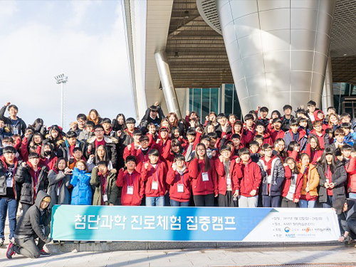 KAIST Intensive Science Camp for Middle-High School Students
The KAIST Global Institute of Talented Education (Director: Dong-Soo Kwon) invited around 90 middle and high school students for an advanced science intensive camp from January 22 to 24.
This camp targeted middle and high school students in community centers or child-care institutions. It aims to increase students’ interest in science and engineering, and assist them with their career paths through programs such as special lectures on science, advanced science projects, and career mentoring.
Participating students were divided into groups of seven or eight with a KAIST student as a mentor to conduct advanced science projects such as VR controller production and robot arm programming. The camp included exploring future career options and science and engineering college admission counselling.
Jiyoung Ryu, Research Professor for the KAIST Global Institute of Talented Education, said, “KAIST started the science and engineering career experience program in 2016 with the Ministry of Education and Korea Research Institute for Vocational Education and Training (KRIVET). So far, 6000 middle and high school students from around the country have participated. The camp is more meaningful since it educates students in social responsibility, in addition to the fields of science and engineering, both of which are missions and goals that KAIST strives for.” She continued to say, “We plan to continue to expand the program in the future.”
The KAIST Global Institute of Talented Education is actively conducting research and projects on national education for talented youth such as policy research concerning gifted education, science and engineering career education, advanced science camps, training for gifted education teachers, and cyber gifted education programs.
2017.02.01 View 8257
KAIST Intensive Science Camp for Middle-High School Students
The KAIST Global Institute of Talented Education (Director: Dong-Soo Kwon) invited around 90 middle and high school students for an advanced science intensive camp from January 22 to 24.
This camp targeted middle and high school students in community centers or child-care institutions. It aims to increase students’ interest in science and engineering, and assist them with their career paths through programs such as special lectures on science, advanced science projects, and career mentoring.
Participating students were divided into groups of seven or eight with a KAIST student as a mentor to conduct advanced science projects such as VR controller production and robot arm programming. The camp included exploring future career options and science and engineering college admission counselling.
Jiyoung Ryu, Research Professor for the KAIST Global Institute of Talented Education, said, “KAIST started the science and engineering career experience program in 2016 with the Ministry of Education and Korea Research Institute for Vocational Education and Training (KRIVET). So far, 6000 middle and high school students from around the country have participated. The camp is more meaningful since it educates students in social responsibility, in addition to the fields of science and engineering, both of which are missions and goals that KAIST strives for.” She continued to say, “We plan to continue to expand the program in the future.”
The KAIST Global Institute of Talented Education is actively conducting research and projects on national education for talented youth such as policy research concerning gifted education, science and engineering career education, advanced science camps, training for gifted education teachers, and cyber gifted education programs.
2017.02.01 View 8257 -
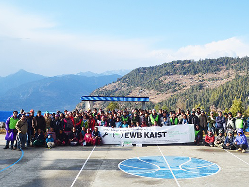 EWB-KAIST Wraps up Five-Year Project in Nepal
‘Engineers Without Borders-KAIST (EWB-KAIST)’ led by Professor Tae-ho Song from the Department of Mechanical Engineering returned to Korea on January 10 after a two-week project in Nangi, Nepal.
EWB-KAIST was established in 2012 by KAIST students and professors. Since then, the team visited Nangi, in the Annapurna region of Nepal, to engage in Appropriate Technology (AT) development projects. The projects included building passive houses and small hydroelectric power, and teaching science education. In particular, passive houses that use straw as an insulator received great a reception from the locals.
This was their last visit to Nepal, since the five-year project has now come to an end. Future projects in Mongolia will be led by Professor Buhm Soon Park from the Graduate School of Science and Technology Policy.
Professor Song commented, “I am glad that the Nepal project was successfully conducted over the last five years. To make sure the support does not end here, I will personally continue to visit the Himalayas to assist the villagers.”
EWB-KAIST is a non-profit organization that conducts activities with the aim of AT development and providing support for less-developed countries in need of the benefits of technology.
( Passive house made of straws by EWB-KAIST team in Nangi, Nepal.)
2017.02.01 View 7357
EWB-KAIST Wraps up Five-Year Project in Nepal
‘Engineers Without Borders-KAIST (EWB-KAIST)’ led by Professor Tae-ho Song from the Department of Mechanical Engineering returned to Korea on January 10 after a two-week project in Nangi, Nepal.
EWB-KAIST was established in 2012 by KAIST students and professors. Since then, the team visited Nangi, in the Annapurna region of Nepal, to engage in Appropriate Technology (AT) development projects. The projects included building passive houses and small hydroelectric power, and teaching science education. In particular, passive houses that use straw as an insulator received great a reception from the locals.
This was their last visit to Nepal, since the five-year project has now come to an end. Future projects in Mongolia will be led by Professor Buhm Soon Park from the Graduate School of Science and Technology Policy.
Professor Song commented, “I am glad that the Nepal project was successfully conducted over the last five years. To make sure the support does not end here, I will personally continue to visit the Himalayas to assist the villagers.”
EWB-KAIST is a non-profit organization that conducts activities with the aim of AT development and providing support for less-developed countries in need of the benefits of technology.
( Passive house made of straws by EWB-KAIST team in Nangi, Nepal.)
2017.02.01 View 7357 -
 Educating for Sustainability: KAIST's Graduate Schools of EEWS and Green Growth
At the World Economic Forum’s (WEF) Annual Meeting (Davos Forum) January 17-20, 2017 in Davos, Switzerland, the International Sustainable Campus Network (ISCN) and the Global University Leaders Forum (GULF) shared exemplary case studies for teaching “sustainability” on campuses, which were implemented by 30 leading universities around the world.
KAIST President Sung-Mo Kang participated in the meeting and introduced two of the university’s graduate schools and their main activities in 2016: The Graduate School of EEWS (energy, environment, water and sustainability) and The Graduate School of Green Growth.
President Kang explained that the EEWS Graduate School, created in 2009, represents KAIST’s commitment to interdisciplinary education and research, addressing key issues of today’s global challenges including energy, environment, and water for a sustainable society. The graduate school hosted its first international forum last October, “The EEWS 2016: Progress and Perspective of Energy Science and Technology.” Over 200 participants from Korea and across the world discussed and learned about recent advances, challenges, and future opportunities in energy science and technology, such as the development of sustainable energy harvesting and storage, catalytic energy conversion technology, green chemical materials, and photocatalytic systems for sustainable water treatment.
He also presented the Green Growth Graduate School as KAIST’s initiative to a build global alliance for sustainable growth. Established in 2013 in the College of Business, the graduate school provides world-class education and research on green business, finance, and policy. Among many international conferences and workshops it hosts, the school has held the Seoul Climate Energy Conference annually since 2014. Last year alone, over 400 international participants including climate and energy policy makers and scholars gathered at the conference and strengthened partnerships with the global community. The school has been an active member of international organizations that advocate for green economies and sustainable development, the Global Green Growth Institute and the United Nations Environment Programme, for example.
President Kang noted that KAIST has been at the forefront of formulating and implementing holistic and cross-disciplinary approaches to foster learning and research environments in which university members can take on global issues, which are critical to humanity and our ecosystem, and work toward a more sustainable future.
Founded in 2007, the ISCN is a non-profit association of globally-leading colleges and universities representing over 30 countries and working together to holistically integrate sustainability into campus operations, research, and teaching.
Created in 2006, the GULF is one of the WEF’s expert communities, which consists of top leaders from 26 global universities, including the University of Cambridge, Peking University, Stanford University, and the Swiss Federal Institute of Technology in Zurich. The GULF offers in-depth discussions and exchange of ideas on the future of higher education and the role of science in society. Since 2012, KAIST has been a member of GULF, the only university from Korea.
The ISCN and GULF have held a meeting each year at the Davos Forum since 2011 to share information, insights, and best practices for achieving sustainable campus operations and integrating sustainability into research and teaching.
To see the full report on the 2017 WEF ISCN-GULF case studies, please go to
http://www.international-sustainable-campus-network.org/downloads/general/462-educating-for-sustainability/file.
2017.01.25 View 9531
Educating for Sustainability: KAIST's Graduate Schools of EEWS and Green Growth
At the World Economic Forum’s (WEF) Annual Meeting (Davos Forum) January 17-20, 2017 in Davos, Switzerland, the International Sustainable Campus Network (ISCN) and the Global University Leaders Forum (GULF) shared exemplary case studies for teaching “sustainability” on campuses, which were implemented by 30 leading universities around the world.
KAIST President Sung-Mo Kang participated in the meeting and introduced two of the university’s graduate schools and their main activities in 2016: The Graduate School of EEWS (energy, environment, water and sustainability) and The Graduate School of Green Growth.
President Kang explained that the EEWS Graduate School, created in 2009, represents KAIST’s commitment to interdisciplinary education and research, addressing key issues of today’s global challenges including energy, environment, and water for a sustainable society. The graduate school hosted its first international forum last October, “The EEWS 2016: Progress and Perspective of Energy Science and Technology.” Over 200 participants from Korea and across the world discussed and learned about recent advances, challenges, and future opportunities in energy science and technology, such as the development of sustainable energy harvesting and storage, catalytic energy conversion technology, green chemical materials, and photocatalytic systems for sustainable water treatment.
He also presented the Green Growth Graduate School as KAIST’s initiative to a build global alliance for sustainable growth. Established in 2013 in the College of Business, the graduate school provides world-class education and research on green business, finance, and policy. Among many international conferences and workshops it hosts, the school has held the Seoul Climate Energy Conference annually since 2014. Last year alone, over 400 international participants including climate and energy policy makers and scholars gathered at the conference and strengthened partnerships with the global community. The school has been an active member of international organizations that advocate for green economies and sustainable development, the Global Green Growth Institute and the United Nations Environment Programme, for example.
President Kang noted that KAIST has been at the forefront of formulating and implementing holistic and cross-disciplinary approaches to foster learning and research environments in which university members can take on global issues, which are critical to humanity and our ecosystem, and work toward a more sustainable future.
Founded in 2007, the ISCN is a non-profit association of globally-leading colleges and universities representing over 30 countries and working together to holistically integrate sustainability into campus operations, research, and teaching.
Created in 2006, the GULF is one of the WEF’s expert communities, which consists of top leaders from 26 global universities, including the University of Cambridge, Peking University, Stanford University, and the Swiss Federal Institute of Technology in Zurich. The GULF offers in-depth discussions and exchange of ideas on the future of higher education and the role of science in society. Since 2012, KAIST has been a member of GULF, the only university from Korea.
The ISCN and GULF have held a meeting each year at the Davos Forum since 2011 to share information, insights, and best practices for achieving sustainable campus operations and integrating sustainability into research and teaching.
To see the full report on the 2017 WEF ISCN-GULF case studies, please go to
http://www.international-sustainable-campus-network.org/downloads/general/462-educating-for-sustainability/file.
2017.01.25 View 9531