AT
-
 Observation of the Phase Transition of Liquid Crystal Defects
KAIST researchers observed the phase transition of topological defects formed by liquid crystal (LC) materials for the first time.
The phase transition of topological defects, which was also the theme of the Nobel Prize for Physics in 2016, can be difficult to understand for a layperson but it needs to be studied to understand the mysteries of the universe or the underlying physics of skyrmions, which have intrinsic topological defects.
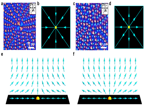
If the galaxy is taken as an example in the universe, it is difficult to observe the topological defects because the system is too large to observe some changes over a limited period of time. In the case of defect structures formed by LC molecules, they are not only a suitable size to observe with an optical microscope, but also the time period in which the phase transition of a defect occurring can be directly observed over a few seconds, which can be extended to a few minutes. The defect structures formed by LC material have radial, circular, or spiral shapes centering on a singularity (defect core), like the singularity that was already introduced in the famous movie "Interstellar,” which is the center point of black hole.
In general, LC materials are mainly used in liquid crystal displays (LCDs) and optical sensors because it is easy to control their specific orientation and they have fast response characteristics and huge anisotropic optical properties. It is advantageous in terms of the performance of LCDs that the defects of the LC materials are minimized. The research team led by Professor Dong Ki Yoon in the Graduate School of Nanoscience and Technology did not simply minimize such defects but actively tried to use the LC defects as building blocks to make micro- and nanostructures for the patterning applications. During these efforts, they found the way to directly study the phase transition of topological defects under in-situ conditions.
Considering the LC material from the viewpoint of a device like a LCD, robustness is important. Therefore, the LC material is injected through the capillary phenomenon between a rigid two-glass plate and the orientation of the LCs can be followed by the surface anchoring condition of the glass substrate. However, in this conventional case, it is difficult to observe the phase transition of the LC defect due to this strong surface anchoring force induced by the solid substrate.
In order to solve this problem, the research team designed a platform, in which the movement of the LC molecules was not restricted, by forming a thin film of LC material on water, which is like oil floating on water. For this, a droplet of LC material was dripped onto water and spread to form a thin film. The topological defects formed under this circumstance could show the thermal phase transition when the temperature was changed. In addition, this approach can trace back the morphology of the original defect structure from the sequential changes during the temperature changes, which can give hints to the study of the formation of topological defects in the cosmos or skyrmions.
Prof. Yoon said, “The study of LC crystal defects itself has been extensively studied by physicists and mathematicians for about 100 years. However, this is the first time that we have observed the phase transition of LC defects directly.” He also added, "Korea is leading in the LCD industry, but our basic research on LCs is not at the world's research level."
The first author of this study is Dr. Min-Jun Gimand supported by a grant from the National Research Foundation (NRF) and funded by the Korean Government (MSIP). The research result was published on May 30, 2017 in Nature Communications.
Figure 1. The phase transition of the LC topological defect on cooling.
Figure 2. Polarizing optical microscopy images of topological defects depending on the strength of the director field. (a,b,e) Convergent director field arrangements of LC molecules and corresponding schematic images; (c,d,f) Divergent director field arrangements of LC molecules and corresponding schematic images.
2017.06.02 View 9936
 -
 Augmented Reality Application for Smart Tour
‘K-Culture Time Machine,’ an augmented and virtual reality application will create a new way to take a tour. Prof. Woon-taek Woo's research team of Graduate School of Culture Technology of KAIST developed AR/VR application for smart tourism.
The 'K-Culture Time Machine' application (iOS App Store app name: KCTM) was launched on iOS App Store in Korea on May 22 as a pilot service that is targetting the Changdeokgung Palace of Seoul.
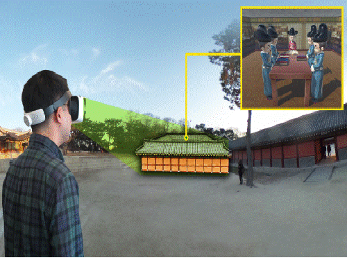
The application provides remote experience over time and space for cultural heritage or relics thorough wearable 360-degree video. Users can remotely experience cultural heritage sites with 360-degree video provided by installing a smartphone in a smartphone HMD device, and can search information on historical figures, places, and events related to cultural heritage. Also, 3D reconstruction of lost cultural heritage can be experienced.
Without using wearable HMD devices, mobile-based cultural heritage guides can be provided based on the vision-based recognition on the cultural heritages. Through the embedded camera in smartphone, the application can identify the heritages and provide related information and contents of the hertages. For example, in Changdeokgung Palace, a user can move inside the Changdeokgung Palace from Donhwa-Gate (the main gate of the Changdeokgung Palace), Injeong-Jeon(main hall), Injeong-Moon (Main gate of Injeong-Jeon), and to Huijeongdang (rest place for the king). Through the 360 degree panoramic image or video, the user can experience the virtual scene of heritages.
The virtual 3D reconstruction of the seungjeongwon (Royal Secretariat) which does not exist at present can be shown of the east side of the Injeong-Jeon The functions can be experienced on a smartphone without a wearable device, and it would be a commercial application that can be utilized in the field once the augmented reality function which is under development is completed.
Professor Woo and his research team constructed and applied standardized metadata of cultural heritage database and AR/VR contents. Through this standardized metadata, unlike existing applications which are temporarily consumed after development, reusable and interoperable contents can be made.Professor Woo said, "By enhancing the interoperability and reusability of AR contents, we will be able to preoccupy new markets in the field of smart tourism."
The research was conducted through the joint work with Post Media (CEO Hong Seung-mo) in the CT R&D project of the Ministry of Culture, Sports and Tourism of Korea. The results of the research will be announced through the HCI International 2017 conference in Canada this July.
Figure 1. 360 degree panorama image / video function screen of 'K-Culture Time Machine'. Smartphone HMD allows users to freely experience various cultural sites remotely.
Figure 2. 'K-Culture Time Machine' mobile augmented reality function screen. By analyzing the location of the user and the screen viewed through the camera, information related to the cultural heritage are provided to enhance the user experience.
Figure 3. The concept of 360-degree panoramic video-based VR service of "K-Culture Time Machine", a wearable application supporting smart tour of the historical sites. Through the smartphone HMD, a user can remotely experience cultural heritage sites and 3D reconstruction of cultural heritage that does not currently exist.
2017.05.30 View 11708
 -
 The 2017 International Food Festival
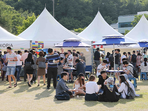
The savory smell of exotic dishes filled the main plaza of the KAIST campus on May 26. Exotic music reverberated throughout the campus. The KAIST community took a break together on a breezy early summer Friday afternoon sharing food with their friends and family. KAIST international student body, KISA (KAIST International Students Association), installed white food tents and prepared their country’s favorite dishes at their 13th annual International Food Festival.
The festival was co-organized with Chungnam National University and the University of Science & Technology (UST). At the festival, students from 18 nations cooked about 60 dishes and sold them to the public. Foreign students’ performances of traditional dance and music on the stage livened the atmosphere.
KISA President Sanzhar Kerimbek of the Department of Chemical and Biomolecular Engineering said, “We are so glad to show the diversity of KAIST and its rich culture. This is a big opportunity to get together with neighboring universities, CNU and UST and say thank you for their participation and support." Valentin Porcellini, an exchange students from France in the School of Computing, said, “We are so excited to have people taste our crepes, ratatouille, and other dishes.”
Associate Vice President of the International Office Jay Hyung Lee also said he was glad to see so many people joining this festival. While congratulating the students on the success of the festival, he said the festival will serve as an opportunity to better understand each other by sharing the food and culture.
(Photo caption: Paricipants stop by the Indonesian booth to purchase the food at the International Food Festival on May 26.)
2017.05.29 View 5890
 -
 Extreme Materials for Fusion with Metal Cocktail
The research team under Professor Ryu Ho-jin of the Department of Nuclear and Quantum Engineering has developed a new material for facing fusion plasma environments using metal powder mixing technology. This technology is expected to extend the range of materials that can be designed for use in extreme environments such as in fusion power generators.
The durability of the tokamak vessel, which holds high-temperature plasma, is very important to create fusion power reactors, which are expected to be a future energy source. Currently, high-melting-point metals, such as tungsten, are considered plasma-facing materials to protect the tokamak vessel. However, high-energy thermal shocks, plasma ions, and neutrons are fatal to the plasma-facing material during high temperature fusion plasma operation. Therefore, it is necessary to develop new high-performance materials.
The ITER project, in which seven countries including the United States, the EU, and Korea participate jointly, is constructing a nuclear fusion experimental reactor in France with the goal of achieving the first plasma in 2025 and deuterium-tritium fusion operation in 2035. In Korea, the KSTAR tokamak at the National Fusion Research Institute has succeeded in maintaining high-performance plasma for 70 seconds.
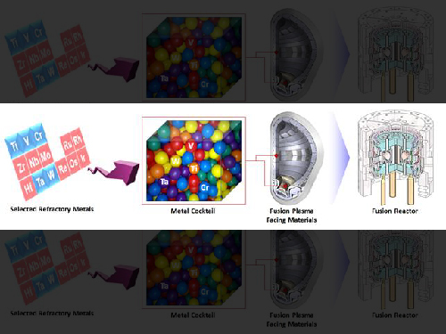
Researchers in Europe, the United States, and China, who are leading the research on fusion plasma-facing materials, are studying the improvement of physical properties by adding a small amount of metal elements to tungsten. However, Professor Ryu’s team reported that by mixing various metals’ powders, including tungsten, they have succeeded in producing a new material that has twice the hardness and strength of tungsten. The difference in the atomic sizes of the well-mixed elements in the alloy is very significant because it makes it difficult to deform the alloy.
The team will continue its research to find alloying compositions that optimize mechanical properties as well as thermal conductivity, plasma interactions, neutron irradiation embrittlement, tritium absorption, and high-temperature oxidation properties.
Professor Ryu said, "Fusion plasma-facing materials are exposed to extreme environments and no metal is capable of withstanding thermal shock, plasma, and neutron damage simultaneously. As a result of this research, attempts to develop complex metallic materials for nuclear fusion and nuclear power are expected to become more active around the world. "
Ph.D. candidate Owais Ahmed Waseem is the first author of this project. The research is supported by the Ministry of Science, ICT and Future Planning, the Korea Research Foundation's Fusion Basic Research project, and the Engineering Research Center. The results were published in 'Scientific Report' on May 16.
Figure 1. Tungsten-based high strengh alloy sample
Figure 2. Fusion plasma facing material development by powder processing of refractory elements
2017.05.26 View 9605
 -
 Controlling 3D Behavior of Biological Cells Using Laser Holographic Techniques
A research team led by Professor YongKeun Park of the Physics Department at KAIST has developed an optical manipulation technique that can freely control the position, orientation, and shape of microscopic samples having complex shapes. The study has been published online in Nature Communications on May 22.
Conventional optical manipulation techniques called “optical tweezers,” have been used as an invaluable tool for exerting micro-scale force on microscopic particles and manipulating three-dimensional (3-D) positions of particles. Optical tweezers employ a tightly-focused laser whose beam diameter is smaller than one micrometer (1/100 of hair thickness), which can generate attractive force on neighboring microscopic particles moving toward the beam focus. Controlling the positions of the beam focus enabled researchers to hold the particles and move them freely to other locations so they coined the name “optical tweezers,” and have been widely used in various fields of physical and biological studies.
So far, most experiments using optical tweezers have been conducted for trapping spherical particles because physical principles can easily predict optical forces and the responding motion of microspheres. For trapping objects having complicated shapes, however, conventional optical tweezers induce unstable motion of such particles, and controllable orientation of such objects is limited, which hinder controlling the 3-D motion of microscopic objects having complex shapes such as living cells.
The research team has developed a new optical manipulation technique that can trap complex objects of arbitrary shapes. This technique first measures 3-D structures of an object in real time using a 3-D holographic microscope, which shares the same physical principle of X-Ray CT imaging. Based on the measured 3-D shape of the object, the researchers precisely calculates the shape of light that can stably control the object. When the shape of light is the same as the shape of the object, the energy of the object is minimized, which provides the stable trapping of the object having the complicated shape.
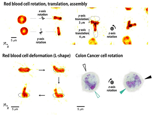
Moreover, by controlling the shape of light to have various positions, directions, and shapes of objects, it is possible to freely control the 3-D motion of the object and make the object have a desired shape. This process resembles the generation of a mold for casting a statue having desired shape so the researchers coined the name of the present technique “tomographic mold for optical trapping (TOMOTRAP).” The team succeeded in trapping individual human red blood cells stably, rotating them with desired orientations, folding them in an L-shape, and assembling two red blood cells together to form a new structure. In addition, colon cancer cells having a complex structure could be stably trapped and rotated at desired orientations. All of which have been difficult to be realized by the conventional optical techniques.
Professor Park said, “Our technique has the advantage of controlling the 3-D motion of complex shaped objects without knowing prior information about their shape and optical characteristics, and can be applied in various fields including physics, optics, nanotechnology, and medical science.”
Dr. Kyoohyun Kim, the lead author of this paper, noted that this technique can induce controlled deformation of biological cells with desired shapes. “This approach can be also applied to real-time monitoring of surgical prognosis of cellular-level surgeries for capturing and deforming cells as well as subcellular organelles,” added Kim.
Figure 1. Concept of optical manipulation techniques
Figure 2. Experimental setup
Figure 3. Research results
2017.05.25 View 8692
 -
 Total Synthesis of Flueggenine C via an Accelerated Intermolecular Rauhut-Currier Reaction
The first total synthesis of dimeric securinega alkaloid (-)-flueggenine C was completed via an accelerated intermolecular Rauhut–Currier (RC) reaction. The research team led by Professor Sunkyu Han in the Department of Chemistry succeeded in synthesizing the natural product by reinventing the conventional RC reaction.
The total synthesis of natural products refers to the process of synthesizing secondary metabolites isolated from living organisms in the laboratory through a series of chemical reactions. Each stage of chemical reaction needs to be successful to produce the final target molecule, and thus the process requires high levels of patience and creativity. For that reason, the researchers working on natural products total synthesis are often called “molecular artists”.
Despite numerous reports on the total synthesis of monomeric securinegas, the synthesis of dimeric securinegas, whose monomeric units are connected by a putative enzymatic RC reaction, has not been reported to date.
The team used a Rauhut-Currier (RC) reaction, a carboncarbon bond forming a reaction between two Michael acceptors first reported by Rauhut and Currier in 1963, to successfully synthesize a dimeric natural product, flueggenine C. This new work featured the first application of an intermolecular RC reaction in total synthesis.
The conventional intermolecular RC reaction was driven non-selectively by a toxic nucleophilic catalyst at a high temperature of over 150°C and a highly concentrated reaction mixture, and thus has never been applied to natural products total synthesis. To overcome this long-standing problem, the research team placed a nucleophilic moiety at the γ-position of the enone derivative. As a result, the RC reaction could be induced by the simple addition of a base at ambient temperature and dilute solution, without the need of a nucleophilic catalyst. Using this newly discovered reactivity, the team successfully synthesized the natural product (-)-flueggenine C from commercially available amino acid derivative in 12 steps.
Professor Han said, “Our key finding regarding the remarkably improved reactivity and selectivity of the intermolecular RC reaction will serve as a significant stepping stone in allowing this reaction to be considered a practical and reliable chemical tool with broad applicability in natural products, pharmaceuticals, and materials syntheses. ”
This research was led by Ph.D. candidate Sangbin Jeon and was published in The Journal of the American Chemical Society (JACS) on May 10. This research was funded by KAIST start-up funds, HRHR (High-Risk High-Return), RED&B (Research, Education, Development & Business) projects, the National Research Foundation of Korea, and the Institute for Basic Science.
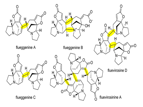
(Figure 1: Representative dimeric/oligomeric securinega alkaloids)
(Figure 2: Our reinvented Rauhut-Currier reaction)
(Figure 3: Total Synthesis of (-)-flueggenine C)
2017.05.23 View 9450
 -
 2017 KAIST Research Day Honors Professor Hoon Sohn
The 2017 KAIST Research Day recognized Professor Hoon Sohn of the Department of Civil and Environmental Engineering as Research Grand Prize Awardee in addition to the 10 most distinguished research achievements of the past year.
The Research Grand Prize recognizes the professor whose comprehensive research performance evaluation indicator is the highest over the past five years. The indicator combines the factors of the number of research contracts, IPR, royalty income, as well as research overhead cost inclusion.
During the ceremony, which was held on May 23, Professor Jun-Ho Oh of the Department of Mechanical Engineering and Professor Sang Yup Lee of the Department of Chemical and Biomolecular Engineering also won the Best Research Award. The two professors had the best scores when evaluating their research performance for one-year periods.
Meanwhile, the Research Innovation Award went to Professor YongKeun Park of the Department of Physics. The Research Innovation Award scores the factors of foreign patent registration, contracts of technological transfer and income from technology fees, technology consultations, and startups and selected Professor Park as the top winner.
Professors Yong Hee Lee of the Department of Physics and Jonghwa Shin of the Department of Material Science won the Convergence Research Award. The Convergence Research Award recognizes the most outstanding research team who created innovative research results for a year.
After the ceremony, President Chen Shiyi of the Southern University of Science and Technology gave a distinguished lecture on the “Global & Entrepreneurial Universities for the Age of the Fourth Industrial Revolution.” the Research Day ceremony, KAIST also presented the ten most distinguished research achievements made by KAIST professors during the last year as follows (Click):
▲ Commercialization of 3D Holographic Microscopy by Professor YongKeun Park of the Department of Physics
▲ Designer Proteins with Chemical Modifications by Professor Hee-Sung Park of the Department of Chemistry
▲ Lanthanum-Catalyzed Synthesis of Microporous 3D Graphene-Like Carbons in a Zeolite Template by Professor Ryong Ryoo of the Department of Chemistry
▲ Complete Prevention of Blood Loss by Self-Sealing Hemostatic Needles by Professor Haeshin Lee of the Department of Chemistry
▲ An Immunological Mechanism for the Contribution of Commensal Microbiota Against Herpes Simplex Virus Infection in Genital Mucosa by Heung Kyu Lee of the Graduate School of Medical Science and Engineering
▲ Development of a Pulse-Echo Laser Ultrasonic Propagation Imaging System by Professor Jung-Ryul Lee of the Department of Aerospace Engineering
▲ Bi-refractive Stereo Imaging for Single-Shot Depth Acquisition by Professor Min H. Kim of the School of Computing
▲ Development of Environment Friendly Geotechnical Construction Material Using Biopolymer by Professor Gye-Chun Cho of the Department of Civil and Environmental Engineering
▲ Protein Delivery Via Engineered Exosomes by Professor Chulhee Choi of the Department of Bio and Brain Engineering
▲ Hot Electron Detection Under Catalytic Reactions by Professor Jeong Young Park of the Graduate School of EEWS.
After the ceremony, President Chen Shiyi of the Southern University of Science and Technology gave a distinguished lecture on the “Global & Entrepreneurial Universities for the Age of the Fourth Industrial Revolution.”
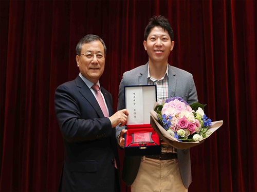
(Photo:President Shin poses with the 2017 KAIST Research Grand Prize Winner Professor Hoon Sohn on May 23.)
2017.05.23 View 13575
 -
 Parasitic Robot System for Turtle's Waypoint Navigation
A KAIST research team presented a hybrid animal-robot interaction called “the parasitic robot system,” that imitates the nature relationship between parasites and host.
The research team led by Professor Phil-Seung Lee of the Department of Mechanical Engineering took an animal’s locomotive abilities to apply the theory of using a robot as a parasite. The robot is attached to its host animal in a way similar to an actual parasite, and it interacts with the host through particular devices and algorithms.
Even with remarkable technology advancements, robots that operate in complex and harsh environments still have some serious limitations in moving and recharging. However, millions of years of evolution have led to there being many real animals capable of excellent locomotion and survive in actual natural environment.
Certain kinds of real parasites can manipulate the behavior of the host to increase the probability of its own reproduction. Similarly, in the proposed concept of a “parasitic robot,” a specific behavior is induced by the parasitic robot in its host to benefit the robot.
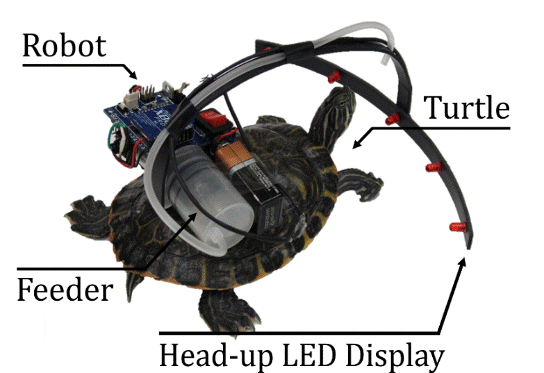
The team chose a turtle as their first host animal and designed a parasitic robot that can perform “stimulus-response training.” The parasitic robot, which is attached to the turtle, can induce the turtle’s object-tracking behavior through repeated training sessions.
The robot then simply guides it using LEDs and feeds it snacks as a reward for going in the right direction through a programmed algorithm. After training sessions lasting five weeks, the parasitic robot can successfully control the direction of movement of the host turtles in the waypoint navigation task in a water tank.
This hybrid animal–robot interaction system could provide an alternative solution of the limitations of conventional mobile robot systems in various fields. Ph.D. candidate Dae-Gun Kim, the first author of this research said that there are a wide variety of animals including mice, birds, and fish that could perform equally as well at such tasks. He said that in the future, this system will be applied to various exploration and reconnaissance missions that humans and robots find it difficult to do on their own.
Kim said, “This hybrid animal-robot interaction system could provide an alternative solution to the limitations of conventional mobile robot systems in various fields, and could also act as a useful interaction system for the behavioral sciences.”
The research was published in the Journal of Bionic Engineering April issue.
2017.05.19 View 10057
 -
 Prof. Sang-Min Bae Receives 2017 iF Design Award
Prof. Sang-Min Bae and his research team from the Industrial Design Department of KAIST submitted a winning entry to the 2017 iF Design Award named ‘Culture BOXCHOOL’.
The iF Design Award is an internationally renowned design contest that is recognized as one of the top three design awards in the world along with the Red Dot Design Award and the IDEA Design Award. It has been held annually by iF International Forum Design since 1953. A total of 5,575 entries from 59 countries entered the last competition.
Culture BOXCHOOL is a modular container space platform designed for culture sharing in isolated areas. It is delivered as a standard shipping container along with its subsidiary modular parts and it transforms into a gallery, office, or classroom. These modular parts build the interior and exterior by attaching them to the corner castings, which are standard parts on all shipping containers. Two Cultural BOXCHOOL containers can be transformed into three different types of layouts.
The containers can generate their own energy using solar panels that provide sustainable energy to equipment inside. Additionally, hot humid air can flow out through the attic vent, doors, and windows.
“With Culture BOXCHOOL, you can easily and quickly create spaces such as offices and classrooms, or you can easily disassemble and move them to another location.
Thus, it can provide everyone with equal educational opportunities and cultural enjoyment regardless of their geographical location. In addition, because it produces its own energy, it is expected to create a cultural space in a relatively harsh environment such as in developing countries. These social and economic values of Culture BOXCHOOL seem to be what led to us winning the contest. I will continue to strive to create the world’s best designs for needy people.” Professor Bae said.
The ID+IM design laboratory, a research team led by Professor Bae, has been studying philanthropy design since 2005, working on solving various problems throughout society through innovative design. They have received more than 50 awards from the most prestigious design competitions in the world.
2017.05.18 View 8286
 -
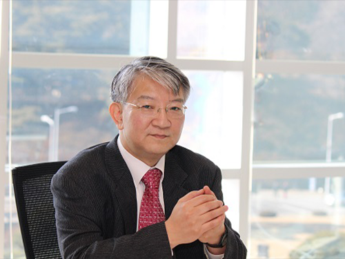 Distinguished Professor Lee Elected to the NAS
Distinguished Professor Sang Yup Lee of the Department of Chemical and Biomolecular Engineering was elected as a foreign associate to the US National Academy of Sciences (NAS) on May 2. The National Academy of Sciences elected 84 new members and 21 foreign associates in recognition of their distinguished and continuing achievements in their original research. Election to the Academy is widely regarded as one of the highest honors that a scientist can receive.
Professor Lee was also elected in 2010 as a member of the US National Academy of Engineering (NAE) for his leadership in microbial biotechnology and metabolic engineering, including the development of fermentation processes for biodegradable polymers and organic acids. Until 2016, there are only 12 people worldwide who are foreign associates of both NAS and NAE.
He is the first Korean elected to both prestigious academies, the NAS and the NAE in the US. Professor Lee is currently the dean of KAIST Institutes, the world leading institute for multi-and interdisciplinary research. He is also serving as co-chair of the Global Council on Biotechnology and member of the Global Future Council on the Fourth Industrial Revolution, the World Economic Forum.
2017.05.16 View 9478
 -
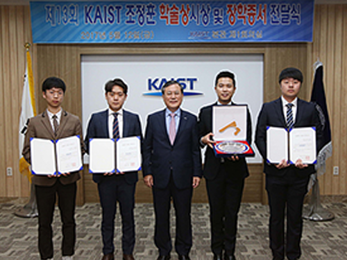 Dr. Zi Jing Wong Named 2017 Jeong Hun Cho Awardee
(Photo caption: The 2017 Jeong Hun Cho Scholarship recipients pose with President Shin (left photo) and Dr. Zi Jing Wong, the recipient of the 2017 Jeong Hun Cho Award)
Dr. Zi Jing Wong, a postdoctoral scholar at the University of California, Berkeley was named the 2017 recipient of the Jeong Hun Cho Award. The award recognizes outstanding young scientists in the field of aerospace engineering annually. The recipient receives a 20 million KRW prize.
The Award Committee said that Dr. Wong who earned his MS at KAIST Department of Aerospace Engineering is a rising scholar in the fields of optic meta materials, photonics, imaging, among others. He has published five papers on the realization of a zero refractive index and the control of a refractive index, as well as the realization of a 3D invisibility cloak in Science and Nature Photonics in 2014 and 2015. Dr. Wong also swept the best paper awards from many international academic societies including the US Materials Research Society, IEEE, SPIE, and Metamaterials Congress in 2015. He finished his Ph.D. at the University of California, Berkeley.
The Award Committee also named three recipients of the Jeong Hun Cho Scholarship: Ph.D. candidate Hyon-Tak Kim of the Department of Aerospace Engineering at KAIST, Ph.D. candidate Ho-Song Park from the Department of Mechanical Engineering at Korea University, and Hyong-Jin Choi of Kongju National University High School.
The award was endowed by the family of the late Ph.D. candidate Jeong Hun Cho who died in a rocket lab accident in the Department of Aerospace Engineering in 2003. Cho was posthumously conferred an honorary doctorate degree.
In memory of Cho, his father established the ‘Jeong Hun Cho Award and Scholarship.’ The scholarship annually selects three young scholars from Cho’s alma maters of KAIST, Korea University, and Kongju National University High School.
2017.05.12 View 11420
 -
 Study Identifies the Novel Molecular Signal for Triggering Septic Shock
Professor Seyun Kim’s team at the Department of Biological Sciences reported the mechanism by which cellular signaling transduction networks are precisely controlled in mediating innate immune responses, such as sepsis, by the enzyme IPMK (Inositol polyphosphate multikinase) which is essential for inositol biosynthesis metabolism.
In collaboration with Professor Hyun Seong Roh at Seoul National University, the study’s first author, Eunha Kim, a Ph.D. candidate in Department of Biological Sciences, performed a series of cellular, biochemical, and physiological experiments searching for the new function of IPMK enzymes in macrophages. The research findings were published in Science Advances on April 21.
Professor Kim’s team has been investigating various inositol metabolites and their biosynthesis metabolism for several years and has multilaterally identified the signaling actions of IPMK for controlling cellular growth and energy homeostasis.
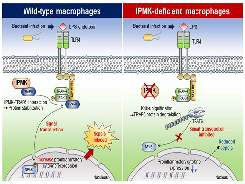
This research showed that the specific deletion of IPMK enzymes in macrophages could significantly reduce levels of inflammation and increase survival rates in mice when they were challenged by microbial septic shock and endotoxins. This suggests a role for IPMK enzymes in mediating innate inflammatory responses that are directly related to a host’s defense against pathogenic bacterial infection.
The team further discovered that IPMK enzymes directly bind to TRAF6 proteins, a key player in immune signaling, thus protecting TRAF6 proteins from ubiquitination reactions that are involved in protein degradation. In addition, Kim and his colleagues successfully verified this IPMK-dependent immune control by employing short peptides which can specifically interfere with the binding between IPMK enzymes and TRAF6 proteins in macrophage cells.
This research revealed a novel function of IPMK enzymes in the fine tuning of innate immune signaling networks, suggesting a new direction for developing therapeutics targeting serious medical conditions such as neuroinflammation, type 2 diabetes, as well as polymicrobial sepsis that are developed from uncontrolled host immune responses. This research was funded by the Ministry of Science, ICT and Future Planning.
(Figure: Deletion of IPMK (inositol polyphosphate multikinase) in macrophages reduces the stability of TRAF6 protein which is the key to innate immune signaling, thereby blocking excessive inflammation in response to pathological bacterial infection.)
2017.05.11 View 9156