ICA
-
 The key to Alzheimer disease, PET-MRI made in Korea
Professor Kyu-Sung Cho
- Simultaneous PET-MRI imaging system commercialization technology developed purely from domestic technology - - Inspiring achievement by KAIST, National NanoFab Center, Sogang University, Seoul National University Hospital –
Hopes are high for the potential of producing domestic products in the field of state-of-the-art medical imaging equipment that used to rely on imported products.
The joint research team (KAIST, Sogang University and Seoul National University) with KAIST Department of Nuclear and Quantum Engineering Professor Kyu-Sung Cho in charge, together with National Nanofab Institution (NNFC; Director Jae-Young Lee), has developed PET-MRI simultaneous imaging system with domestic technology only. The team successfully acquired brain images of 3 volunteers with the newly developed system.
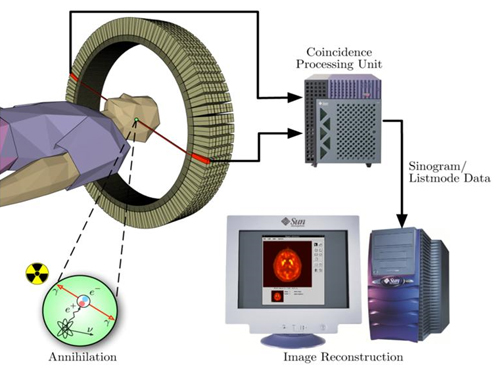
PET-MRI is integrated state-of-the-art medical imaging equipment that combines the advantages of Magnetic Resonance Imaging (MRI) that shows anatomical images of the body and Position Emission Tomography (PET) that analyses cell activity and metabolism. Since the anatomical information and functional information can be seen simultaneously, the device can be used to diagnose early onset Alzheimer’s disease and is essential in biological science research, such as new medicine development.
The existing equipment used to take MRI and PET images separately due to the strong magnetic field generated by MRI and combine the images. Hence, it was time consuming and error-prone due to patient’s movement. There was a need to develop PET that functions within a magnetic field to create a simultaneous imaging system.
The newly developed integral PET-MRI has 3 technical characteristics: 1. PET detector without magnetic interference, 2. PET-MRI integration system, 3.PET-MRI imaging processing.
The PET detector is the most important factor and accounts for half the cost of the whole system. KAIST Professor Cho and NNFC Doctor Woo-Suk Seol’s team successfully developed the Silicon Photomultiplier (amplifies light coming into the radiation detector) that can be used in strong magnetic fields. The developed sensor has a global competitive edge since it optimises semiconductor processing to yield over 95% productivity and around 10% gamma radiation energy resolving power.
Sogang University Department and Electrical Engineering Professor Yong Choi developed cutting edge PET system using a new concept of electric charge signal transmission method and imaging location distinction circuit. The creativity and excellence of the research findings were recognised and hence published on the cover of Medical Physics in June.
Seoul National University Hospital Department of Nuclear Medicine Professor Jae-Sung Lee developed the Silicon Photomultiplier sensor based PET imaging reconstitution programme, MRI imaging based PET imaging revision technology and PET-MRI imaging integration software.
Furthermore, KAIST Department of Electrical Engineering Professor Hyun-Wook Park was responsible for the development of RF Shielding technology that enables simultaneous installation of PET and MRI and using this technology, he developed a head coil for the brain that can be connected to PET for installation.
Based on the technology describe above, the joint research team successfully developed PET-MRI system for brains and acquired PET-MRI integrated brain images from 3 volunteers last June.
In particular, this system has the distinct feature of a detachable PET module and MRI head coil to the existing whole body MRI, so that PET-MRI simultaneous imaging is possible with low installation cost.
Professor Cho said, “We have prepared the foundation of domestic commercial PET and the system has a competitive edge in the global market of PET-MRI system technology.” He continued, “It can reduce the cost of the increasing brain related disease diagnosis, including Alzheimer’s, dramatically.”
Funded by Ministry of Trade, Industry and Energy as an Industrial Foundation Technology Development Project (98 billion won in 7 years), the research applied for over 20 patents and 20 CSI theses.
Figure 1.Brain phantom images from developed PET-MRI system
Figure 2. Brain images from developed PET-MRI system
Figure 3. Domestic PET-MRI clinical trial
Figure 4. Head RF coil and PET detector inserted in MRI
Figure 5. Insertion type PET detector module
Figure 6. Silicon Photomultiplier sensor (Left) and flash crystal block (right)
Figure7. Silicon Photomultiplier sensor
Figure 8. PET detection principle
2013.11.28 View 13892
 -
 Green Technology for Data Centers: Ultra-low Power 100 Gbps Ethernet Integrated Circuit Developed
A new integrated circuit (IC), consuming only 0.75W of electricity, will reduce the power usage of data chips installed at data centers by one-third.
Each day, billions of people surf the Internet for information, entertainment, and educational content. The Internet contains an immeasurable amount of information and knowledge generated every minute all around the world that is readily available to everyone with a click of a computer mouse. The real magic of the Internet, however, lies in data centers, where hundreds of billions of data are stored and distributed to designated users around the clock.
Today, almost every business or organization either has its own data centers or outsources data center services to a third party. These centers house highly specialized equipment responsible for the support of computers, networks, data storage, and business security. Accordingly, the operational cost of data centers is tremendous because they consume a large amount of electricity.
Data centers can consume up to 100 times more energy than a standard office building. Data center energy consumption doubled from 2000 to 2006, reaching more than 60 billion kilowatt hours per year. If the current usage and technology trends continue, the energy consumption of data centers in the US will reach 8% of the country’s total electric power consumption by 2020.
A research team at the Korea Advanced Institute of Science and Technology (KAIST) and Terasquare, Inc. (
http://www.terasquare.co.kr
), a spin-off company of the university,
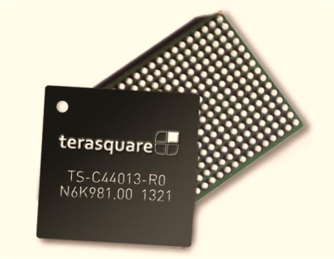
developed an extremely low-powered integrated circuit for Ethernet that consumes less than 0.75W of electricity but is able to send and receive data at the high speed of 100 gigabits per second (Gbps). The research team, headed by Hyeon-Min Bae, assistant professor of electrical engineering at KAIST, claims that the new microchip uses only one-third of the electricity consumed by the currently installed chips at data centers, thereby helping the centers to save energy.
Integrated circuits are embedded on communication modules that are inserted into a line card. Data centers have numerous line cards to build a network including routers and switches. Currently, 8W ICs are the most common in the market, and they consume a lot of energy and require the largest modules (112 cm
2
of CFP), decreasing the port density of line cards and, thus, limiting the amount of data transmission.
The ultra-low-power-circuit, 100-gigabit, full-transceiver CDR, is the world’s first solution that can be loaded to the smallest communication modules (20 cm
2
of CFP4 or 16 cm
2
of
QSFP28), the next-generation chips for data centers. Compared with other chip producers, the 100 Gbps CDR is a greener version of the technology that improves the energy efficiency of data centers while maintaining the high speed of data transmission.
Professor Hyeon-Min Bae said, “When we demonstrate our chip in September of this year at one of the leading companies that manufacture optical communication components and systems, they said that our product is two years ahead of those of our competitors. We plan to produce the chip from 2014 and expect that it will lead the 100 Gbps Ethernet IC market, which is expected to grow to USD 1 billion by 2017.”
The commercial model of the IC was first introduced at the 39
th
European Conference and Exhibition on Optical Communication (ECOC), the largest optical communication forum for new results and developments in Europe, held from September 22-26 at ExCeL London, an international exhibition and convention center.
Professor Bae added, “We received positive responses to our ultra-low-power 100-Gbps Ethernet IC at the ECOC. The chip will be used not only for a particular industry but also for many of next-generation, super-high-speed information communications technologies, such as high-speed USB, high-definition multimedia interface (HDMI), and TV interface.”
Before joining KAIST, Hyeon-Min Bae worked for many years at Finisar as a researcher who designed and developed the world’s first super-high-speed circuit, the 100 Gbps Ethernet IC.
2013.11.25 View 9455
 -
 Professor Chun-Taek Rim Appointed as Associate Editor for IEEE TPEL
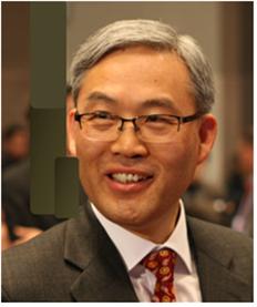
Professor Chun-Taek Rim of the nuclear and quantum engineering at KAIST was appointed as an associate editor of the Institute of Electrical and Electronics Engineers (IEEE) Transactions on Power Electronics (TPEL), an eminent academic journal bio-monthly published in the field of power electronics.The journal has a high impact factor (4.08), a measure reflecting the average number of citations to recent articles published in an academic journal, which ranks as the 6th the most influential journal among the 100 journals published by IEEE.Professor Rim was also appointed to an associate editor for IEEE Journal of Emerging and Selected Topics in Power Electronics in September in recognition of his expertise in wireless power and electric vehicles.
2013.11.15 View 10869
 -
 KAIST student wins Aerospace Student Papers Grand Prize
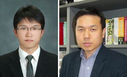
Dong-Il Yoo, a doctoral candidate under Professor Hyun-Chul Shim, at the Department of Aerospace Engineering, KAIST, has been awarded the Second Prize Award at the 11th Korea Aerospace Industries (KAI) Paper Contest. The award ceremony was held on October 30th at the media conference room at the KINTEX ADEX 2013 Exhibition in Seoul.
Yoo"s paper, titled "A Study on Virtual Pursuit Point-based Autonomous Air Combat Guidance Law for UCAV," is highly regarded for originality and creativity. The Field Robotics Center at the KAIST Institute, where Yoo conducted his research, also received the first prize at the 7th KAI Paper Contest.
The KAI Paper Contest was first organized in 2003 to promote academic interest and advance research and development in aerospace engineering among university students.
The KAI Paper Contest is one of the most prestigious contests in Korea. It is sponsored by the Ministry of Trade, Industry and Energy, the Ministry of Land, Infrastructure and Transport, the Korean Society for Aeronautical and Space Sciences, the Korea Aerospace Industries Association, and the Korea Civil Aviation Development Association.
Dong-Il Yoo (left) and Professor Hyun-Chul Shim (right)
2013.11.11 View 12658
 -
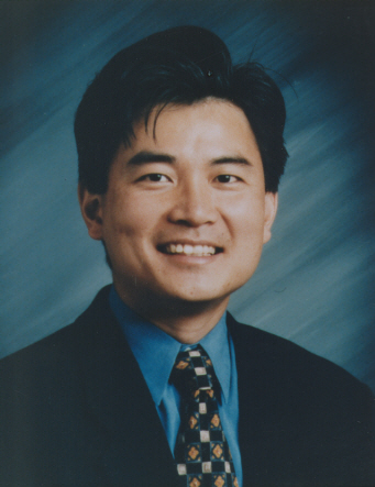 Professor Jae-Hyung Lee appointed as AIChE fellow
Professor Jae-Hyung Lee from the Department of Chemical and Bimolecular Engineering at KAIST was appointed as a fellow in the American Institute of Chemical Engineers (AIChE).
Established in 1908, AIChE is the largest association of chemical engineers worldwide, which now boasts more than 40,000 members from 90 countries.
Following Distinguished Professor Sang Yup Lee from the same department at KAIST, Professor Jae-Hyung Lee is the second Korean appointed as a fellow by the organization.
He has been acknowledged for his innovative research on the improvement of model predictive control of industrial processes.
Professor Lee is the director of the Saudi Armaco-KAIST CO2 Management Center at KAIST, a fellow of the Institute of Electrical and Electronics Engineers (IEEE) and the International Federation of Automatic Control (IFAC), and a member of the Korean Academy of Science and Technology.
He received the Young Investigator Award from the National Science Foundation (NSF) in 1994 and the Computing in Chemical Engineering Award from AIChE in 2013.
2013.11.05 View 9767
 -
 Ultra-High Strength Metamaterial Developed Using Graphene
New metamaterial has been developed, exhibiting hundreds of times greater strength than pure metals.
Professor Seung Min, Han and Yoo Sung, Jeong (Graduate School of Energy, Environment, Water, and Sustainability (EEWS)) and Professor Seok Woo, Jeon (Department of Material Science and Engineering) have developed a composite nanomaterial. The nanomaterial consists of graphene inserted in copper and nickel and exhibits strengths 500 times and 180 times, respectively, greater than that of pure metals. The result of the research was published on the July 2nd online edition in Nature Communications journal.
Graphene displays strengths 200 times greater than that of steel, is stretchable, and is flexible. The U.S. Army Armaments Research, Development and Engineering Center developed a graphene-metal nanomaterial but failed to drastically improve the strength of the material.
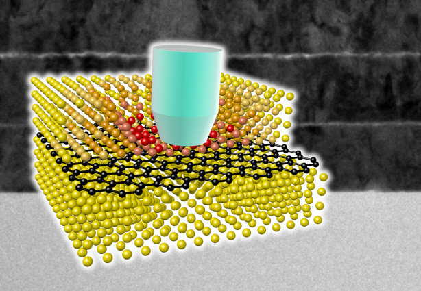
To maximize the strength increased by the addition of graphene, the KAIST research team created a layered structure of metal and graphene. Using CVD (Chemical Vapor Deposition), the team grew a single layer of graphene on a metal deposited substrate and then deposited another metal layer. They repeated this process to produce a metal-graphene multilayer composite material, utilizing a single layer of graphene. Micro-compression tests within Transmission Electronic Microscope and Molecular Dynamics simulations effectively showed the strength enhancing effect and the dislocation movement in grain boundaries of graphene on an atomic level.
The mechanical characteristics of the graphene layer within the metal-graphene composite material successfully blocked the dislocations and cracks from external damage from traveling inwards. Therefore the composite material displayed strength beyond conventional metal-metal multilayer materials. The copper-graphene multilayer material with an interplanar distance of 70nm exhibited 500 times greater (1.5GPa) strength than pure copper. Nickel-graphene multilayer material with an interplanar distance of 100nm showed 180 times greater (4.0GPa) strength than pure nickel.
It was found that there is a clear relationship between the interplanar distance and the strength of the multilayer material. A smaller interplanar distance made the dislocation movement more difficult and therefore increased the strength of the material. Professor Han, who led the research, commented, “the result is astounding as 0.00004% in weight of graphene increased the strength of the materials by hundreds of times” and “improvements based on this success, especially mass production with roll-to-roll process or metal sintering process in the production of ultra-high strength, lightweight parts for automobile and spacecraft, may become possible.” In addition, Professor Han mentioned that “the new material can be applied to coating materials for nuclear reactor construction or other structural materials requiring high reliability.”
The research project received support from National Research Foundation, Global Frontier Program, KAIST EEWS-KINC Program and KISTI Supercomputer and was a collaborative effort with KISTI (Korea Institute of Science and Technology Information), KBSI (Korea Basic Science Institute), Stanford University, and Columbia University.
A schematic diagram shows the structure of metal-graphene multi-layers. The metal-graphene multi-layered composite materials, containing a single-layered graphene, block the dislocation movement of graphene layers, resulting in a greater strength in the materials.
2013.08.23 View 16030
 -
 Prof. Song Chong received the IEEE William R. Bennett Prize Paper Award
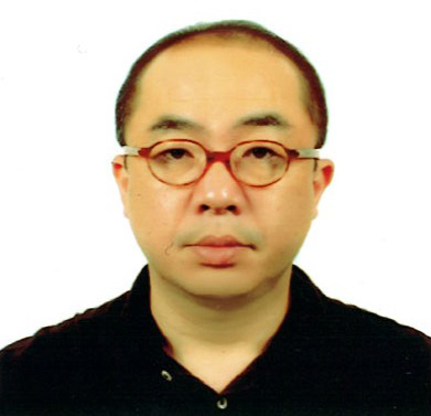
The IEEE (Institute of Electrical and Electronics Engineers) Communications Society (ComSoc), a renowned global network of professionals with a common interest in advancing communications technologies, has announced the winner of the 2013 William R. Bennett Prize in the field of communications networking. The prize was given to a Korean research team led by Song Chong, Professor of Electrical Engineering at KAIST and Injong Rhee, Professor of Computer Science at North Carolina State University. In addition, Dr. Minsu Shin, Dr. Seongik Hong, and Dr. Seong Joon Kim of Samsung Electronics Co., Ltd. as well as Professor Kyunghan Lee from Ulsan National Institute of Science and Technology were recognized for their contribution.
The William R. Bennett Prize for communications networking has been awarded each year since 1994 in recognition of the best paper published in any journal financially sponsored or co-sponsored by ComSoc in the previous three calendar years. Only one paper per year is selected based on its quality, originality, scientific citation index, and peer reviews. Among the previous award winners are Robert Gallager of MIT, and Steven Low of the California Institute of Technology, and Kang G. Shin of the University of Michigan.
The Korean research team’s paper, On the Levy-Walk Nature of Human Mobility, was published in the June 2011 issue of IEEE/ACM Transactions on Networking, a bimonthly journal co-sponsored by the IEEE ComSoc, the IEEE Computer Society, and the Association for Computing Machinery (ACM) with its Special Interest Group on Data Communications (SIGCOMM).
In the paper, the research team proposed a new statistical model to effectively analyze the pattern of individual human mobility in daily life. The team handed out GPS (global positioning system) devices to 100 participants residing in five different university campuses in Korea and the US and collected data on their movements for 226 days. The mobility pattern obtained from the experiment predicted accurately how the participants actually moved around during their routines. Since publication, the paper has been cited by other papers approximately 350 times.
The team’s research results will apply to many fields such as the prevention and control of epidemics, the design of efficient communications networks, and the development of urban and transportation system.
The research team received the award on June 10th at the 2013 IEEE International Conference on Communications (ICC) held in Budapest, Hungary, from June 9-13, 2013.
Professor Song Chong
2013.07.06 View 13658
 -
 KAIST Placed 3rd in the World's Best 100 Emerging Universities
The Times Higher Education (THE) published its world university rankings on June 20, 2013. It is a list of the best 100 universities whose histories are 50 years old or younger. KAIST was ranked 3rd in the list, two places up from the 5th last year. Forbes and Reuters carried a story on the top ten emerging universities out of the listed 100 institutions, highlighting strong showings in the Asian region. For the articles, please see the attached file (Forbes) or click the link (Reuters) below:
http://www.reuters.com/article/2013/06/19/education-university-rankings-idUSL2N0EU1HZ20130619
2013.06.22 View 7669
 -
 Professor Jay H. Lee to receive the 2013 AIChE CAST Computing in Chemical Engineering Award
Professor Jay H. Lee of Chemical and Biomolecular Engineering Department at KAIST has won the 2013 Computing in Chemical Engineering Award of AIChE"s CAST Division (AIChE, American Institute of Chemical Engineers and CAST, Computing & Systems Technology Division).
The CAST Computing in Chemical Engineering Award, sponsored by The Dow Chemical Company, is annually given to an individual who has made outstanding contributions in the application of computing and systems technology to chemical engineering.Professor Lee has been recognized for his pioneering research contributions for “novel paradigms for much improved and robust model predictive control in industrial processes.” He is currently the Head of Chemical and Biomolecular Engineering Department and Director of Brain Korea (BK) 21 Program at the department. BK21 is the Korean government’s initiative to support the growth of research universities in the nation and foster highly trained master’s and doctoral students as well as researchers.
The CAST Computing in Chemical Engineering Award will be presented to Professor Jay H. Lee at the CAST Division dinner to be held at the AIChE Annual Meeting this November in San Francisco, where he will also deliver the after dinner lecture associated with this award.
2013.06.12 View 10445
 -
 KAIST Department of Mechanical Engineering Ranked in 19th Place
- Ranked in 19th place in 2013 Quacquarelli Symonds (QS) World University Rankings by Engineering, Mechanical, Aeronautical and Manufacturing Subjects -
KAIST ranked 19th in 2013 QS World University Rankings by Subject in Engineering, Mechanical, Aeronautical and Manufacturing Subjects. This is great progress compared to last year’s 51st-100th rank.
The 2013 QS World University Rankings used four indicators, including academic reputation, employer reputation, citations per paper, and H-index citations, to assess 2,858 universities in the world, and evaluated up to 200th place in 30 academic subjects.
KAIST earned high remarks from the H-index citations indicator, which is a new criteria introduced in the employer reputation rating. Moreover, the employer reputation section has risen sharply compared to the previous year. The H-index measures qualitatively and quantitatively the research outcomes of the researchers and assesses the number of papers written per professor and the average citation frequency of the papers.
The proportions of the indicators differ by subjects. For the mechanical engineering field, they weigh 40%, 30%, 15%, and 15%, respectively.
Rank
Academic
Employer
Citations per paper
H-index Citations
Score
19 (51-100)
68.1 (78.9)
89.1 (60.2)
84.6 (83.1)
93.1 (N/A)
80.4 (74.6)
2013.06.10 View 7713
 -
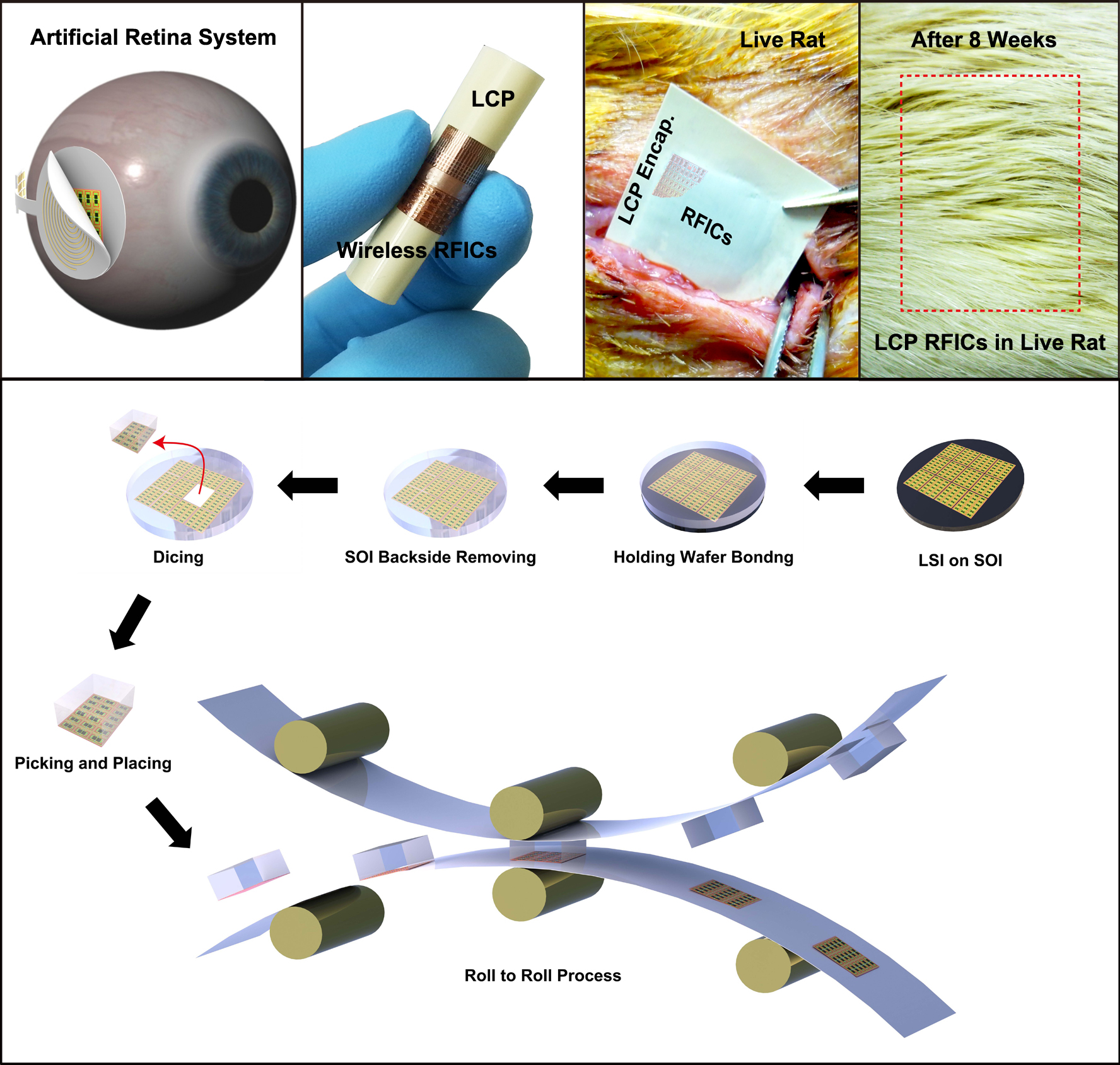 A KAIST research team developed in vivo flexible large scale integrated circuits
Daejeon, Republic of Korea, May 6th, 2013–-A team led by Professor Keon Jae Lee from the Department of Materials Science and Engineering at KAIST has developed in vivo silicon-based flexible large scale integrated circuits (LSI) for bio-medical wireless communication.
Silicon-based semiconductors have played significant roles in signal processing, nerve stimulation, memory storage, and wireless communication in implantable electronics. However, the rigid and bulky LSI chips have limited uses in in vivo devices due to incongruent contact with the curvilinear surfaces of human organs. Especially, artificial retinas recently approved by the Food and Drug Administration (refer to the press release of FDA"s artificial retina approval) require extremely flexible and slim LSI to incorporate it within the cramped area of the human eye.
Although several research teams have fabricated flexible integrated circuits (ICs, tens of interconnected transistors) on plastics, their inaccurate nano-scale alignment on plastics has restricted the demonstration of flexible nano-transistors and their large scale interconnection for in vivo LSI applications such as main process unit (MPU), high density memory and wireless communication. Professor Lee"s team previously demonstrated fully functional flexible memory using ultrathin silicon membranes (Nano Letters, Flexible Memristive Memory Array on Plastic Substrates), however, its integration level and transistor size (over micron scale) have limited functional applications for flexible consumer electronics.
Professor Keon Jae Lee"s team fabricated radio frequency integrated circuits (RFICs) interconnected with thousand nano-transistors on silicon wafer by state-of-the-art CMOS process, and then they removed the entire bottom substrate except top 100 nm active circuit layer by wet chemical etching. The flexible RF switches for wireless communication were monolithically encapsulated with biocompatible liquid crystal polymers (LCPs) for in vivo bio-medical applications. Finally, they implanted the LCP encapsulated RFICs into live rats to demonstrate the stable operation of flexible devices under in vivo circumstances.
Professor Lee said, "This work could provide an approach to flexible LSI for an ideal artificial retina system and other bio-medical devices. Moreover, the result represents an exciting technology with the strong potential to realize fully flexible consumer electronics such as application processor (AP) for mobile operating system, high-capacity memory, and wireless communication in the near future."
This result was published in the May online issue of the American Chemical Society"s journal, ACS Nano (In vivo Flexible RFICs Monolithically Encapsulated with LCP). They are currently engaged in commercializing efforts of roll-to-roll printing of flexible LSI on large area plastic substrates.
Movie at Youtube Link: Fabrication process for flexible LSI for flexible display, wearable computer and artificial retina for in vivo biomedical application
http://www.youtube.com/watch?v=5PpbM7m2PPs&feature=youtu.be
Applications of in Vivo Flexible Large Scale Integrated Circuits
Top: In vivo flexible large scale integrated circuits (LSI); Bottom: Schematic of roll-to-roll printing of flexible LSI on large area plastics.
2013.06.09 View 13809
 -
 Neurotransmitter protein structure and operation principle identified
Professor Tae-Young Yoon
- Real-time measurement of structural change of bio-membrane fusion protein
- A new clue to degenerative brain diseases research
KAIST Physics Department’s Professor Tae-Young Yoon has successfully identified the hidden structure and operation mechanism of the SNARE protein, which has a central role in transporting neurotransmitters between neurons, using magnetic nanotweezers. SNARE protein’s cell membrane fusion function is closely related to degenerative brain diseases or neurological disorders such as Alzheimer’s. Hence, this research may provide a clue to the disease’s prevention and treatment.
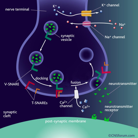
Neurotransmission occurs when vesicles containing neurotransmitters fuse with cell membranes in neuron synapses. The SNARE protein is a cell-membrane fusion protein with a core role of releasing neurotransmitters. The academia speculated the SNARE protein would regulate the exchange of neurotransmitters, but its precise function and structure has been unknown. Professor Yoon’s research team developed an experimental technique using nanotweezers to measure physical changes to nanometer level by pulling and releasing each protein with force of 1 pN (piconewton). The research identified the existence of hidden SNARE protein"s intermediate structure. The process of withstanding and maintaining repulsive forces between bio-membranes in the hidden intermediate structure of SNARE to regulate the exchange of neurotransmitters has also been identified.
Professor Yoon’s research team developed an experimental technique using magnetic nanotweezers to measure physical changes of proteins to nanometer level by pulling and releasing each protein with force of 1 pN. The research identified the existence of hidden SNARE protein"s intermediate structure and its formation. The process of withstanding and maintaining repulsive forces between bio-membranes in the hidden intermediate structure of SNARE to regulate the exchange of neurotransmitters has also been discovered.
Professor Yoon said, “Ground breaking research results have been produced. A simple experimental technique of applying the smallest possible forces to proteins (with tweezers) to see their hidden structure and formation process can produce the same result as real observation has been developed.” He continued, “This technique will be very important in researching biological object with physical experimental technique. It will be a vital foundation to consilient research of different academia in the future.”
This research was a joint project of Physics Department’s Professor Tae-Young Yoon, KAIST, and Biomedical Engineering Institute’s Professor Yeon-Kyun Shin at KIST. KAIST Physics Department’s Professor Yong-Hoon Cho, Ph.D. candidate Do-Yong Lee and KIAS Computational Sciences Department’s Professor Chang-Bong Hyun participated. The research was published on Nature Communications on April 16th.
a) Neurotransmission occurs when vesicles containing neurotransmitters fuse with cell membranes in neuron synapses. A SNARE protein is a cell-membrane fusion protein with a core role of releasing neurotransmitters.
b) A schematic diagram using magnetic nanotweezers to measure protein structure changes on molecular level. The nanotweezers exert an exquisite pull and release of each protein with a force of 1 pN to measure physical changes to nanometer level in real-time to observe the hidden intermediate structure and operation principles of bio-membrane fusion protein.
2013.05.25 View 9419