American+Chemical+Society
-
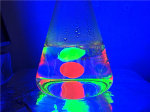 Quantum Dot Film Can Withstand High Temperatures and Humidity
The joint KAIST research team of Professor Byeong-Soo Bae of the Department of Materials Science and Engineering and Professor Doh Chang Lee of the Department of Chemical and Biomolecular Engineering was able to fabricate a siloxane-encapsulated quantum dot film, which exhibits stable emission intensity over one month even at high temperatures and humidity.
The results of this study were published in the Journal of the American Chemical Society (JACS) on November 29, 2016. The research article is entitled “Quantum Dot/Siloxane Composite Film Exceptionally Stable against Oxidation under Heat and Moisture.” (DOI: 10.1021/jacs.6b10681)
Quantum dots (QDs), light-emitting diodes (LEDs) for next-generation displays, are tiny particles or nanocrystals of semiconducting materials. Their emission wavelength can easily be adjusted by changing their sizes, which are just a few nanometers. A wide spectrum of their colors can also achieve ultra-high definition displays.
Due to these characteristics, QDs are coated on a film as a polymer resin in dispersed form, or they are spread on an LED light source. They are thus considered to be crucial for next generation displays.
Despite their exceptional optical properties, however, QDs are easily oxidized in a high temperature and high humidity environment, and, as a result, this greatly deteriorates their luminescence quality (quantum efficiency). Therefore, they are encapsulated in an extra thin layer to block oxygen and moisture.
QD displays in the current market have a film inserted to separate them from LEDs, which create heat. The high unit cost of this protective layer, however, increases the overall cost of displays, lowering their price competitiveness in the market.
For a solution, the research team applied the sol-gel condensation reaction of silane precursors with QDs. This technology uses the reactions of chemical substances to synthesize ceramics or glass at a low temperature.
The team applied QDs in a heat resistant siloxane polymer by employing this technology. The siloxane resin acted as a cup holding the QDs and also blocked heat and moisture. Thus, their performance can be maintained without an extra protective film.
QDs are evenly dispersed into the resin from a chemical process to fabricate a QD embedded film and retained the high quality luminescence not only at a high temperature of 85°C and in a high humidity of 85%, but also in a high acid and high base environment. Remarkably though, the luminescence actually increased in the high humidity environment.
If this technology is used, the overall price of displays will decrease by producing a stable QD film without an extra protective barrier. In the future, the QD film can be directly applied to a blue LED light source. As a result, it will be possible to develop a QD display that can reduce the amount of QDs needed and improve its performance.
Professor Bae said, “We have proposed a way to make quantum dots overcome their limitations and have wide applications as they are being developed for next-generation displays. Our technology will make significant contributions to the display industry in the country.”
He also added, “In the future, we plan to cooperate with companies both in and out of the country to improve the performance of quantum dots and concentrate on their commercialization.”
The research team is currently applying for related patents both in and out of the country. The team is also plan ning to transfer the patents to Sol Ip Technology Inc., a company founded at KAIST, to start the commercialization.
Picture 1:
Siloxane-encapsulated quantum dot (QD) films showing performance stability in boiling water
Picture 2 and 3:
So-gel condensation reaction in silane precursors between Methacryloxypropyltrimethoxysilane (MPTS) and diphenylsilanediol (DPSD). The inset shows photographs of a QD-oligosiloxane resin under room light (left) and a UV lamp (λ = 365 nm) (right).
Free radical addition reactions among carbon double bonds of methacryl functional groups and oleic acids. The inset shows photographs of a QD-silox film under room light (left) and a UV lamp (λ = 365 nm) (right).
2017.02.24 View 11084
 -
 An Improved Carbon Nanotube Semiconductor
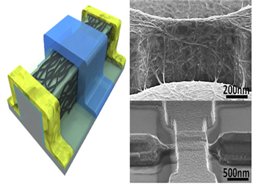
Professor Yang-Kyu Choi and his research team of the School of Electrical Engineering at KAIST collaborated with Professor Sung-Jin Choi of Kookmin University to develop a large-scale carbon nanotube semiconductor by using a 3-D fin-gate structure with carbon nanotubes on its top.
Dong Il Lee, a postdoctoral researcher at KAIST’s Electrical Engineering School, participated in this study as the first author. It was published in ACS Nano on November 10, 2016, and was entitled “Three-Dimensional Fin-Structured Semiconducting Carbon Nanotube Network Transistor.”
A semiconductor made with carbon nanotubes operates faster than a silicon semiconductor and requires less energy, yielding higher performance.
Most electronic equipment and devices, however, use silicon semiconductors because it is difficult to fabricate highly purified and densely packed semiconductors with carbon nanotubes (CNTs).
To date, the performance of CNTs was limited due to their low density. Their purity was also low, so it was impossible to make products that had a constant yield on a large-surface wafer or substrate. These characteristics made the mass production of semiconducting CNTs difficult.
To solve these difficulties, the research team used a 3-D fin-gate to vapor-deposit carbon nanotubes on its top. They developed a semiconductor that had a high current density with a width less than 50 nm.
The three-dimensional fin structure was able to vapor-deposit 600 carbon nanotubes per micrometer. This structure could have 20 times more nanotubes than the two dimensional structure, which could only vapor-deposit thirty in the same 1 micrometer width.
In addition, the research team used semi-conductive carbon nanotubes having a purity rating higher than 99.9% from a previous study to obtain a high yield semiconductor.
The semiconductor from the research group has a high current density even with a width less than 50 μm. The new semiconductor is expected to be five times faster than a silicon-based semiconductor and will require five times less electricity during operation.
Furthermore, the new semiconductor can be made by or will be compatible with the equipment for producing silicon-based semiconductors, so there will be no additional costs.
Researcher Lee said, “As a next generation semiconductor, the carbon nanotube semiconductor will have better performance, and its effectiveness will be higher.” He also added, “Hopefully, the new semiconductor will replace the silicon-based semiconductors in ten years.”
This study received support from the Center for Integrated Smart Sensors funded by the Ministry of Science, ICT & Future Planning of Korea as the Global Frontier Project, and from the CMOS (Complementary Metal-Oxide-Semiconductor) THz Technology Convergence Center of the Pioneer Research Center Program sponsored by the National Research Foundation of Korea.
Picture 1: 3D Diagram of the Carbon Nanotube Electronic Device and Its Scanning Electron Microscope (SEM) Image
Picture 2: 3D Transistor Device on an 8-inch Base and the SEM Image of Its Cross Section
2017.02.16 View 12198
 -
 Extremely Thin and Highly Flexible Graphene-Based Thermoacoustic Speakers
A joint research team led by Professors Jung-Woo Choi and Byung Jin Cho of the School of Electrical Engineering and Professor Sang Ouk Kim of the Material Science and Engineering Department, all on the faculty of the Korea Advanced Institute of Science and Technology (KAIST), has developed a simpler way to mass-produce ultra-thin graphene thermosacoustic speakers.
Their research results were published online on August 17, 2016 in a journal called Applied Materials & Interfaces. The IEEE Spectrum, a monthly magazine published by the Institute of Electrical and Electronics Engineers, reported on the research on September 9, 2016, in an article titled, “Graphene Enables Flat Speakers for Mobile Audio Systems.” The American Chemical Society also drew attention to the team’s work in its article dated September 7, 2016, “Bringing Graphene Speakers to the Mobile Market.”
Thermoacoustic speakers generate sound waves from temperature fluctuations by rapidly heating and cooling conducting materials. Unlike conventional voice-coil speakers, thermoacoustic speakers do not rely on vibrations to produce sound, and thus do not need bulky acoustic boxes to keep complicated mechanical parts for sound production. They also generate good quality sound in all directions, enabling them to be placed on any surface including curved ones without canceling out sounds generated from opposite sides.
Based on a two-step, template-free fabrication method that involved freeze-drying a solution of graphene oxide flakes and the reduction/doping of oxidized graphene to improve electrical properties, the research team produced a N-doped, three-dimensional (3D), reduced graphene oxide aerogel (N-rGOA) with a porous macroscopic structure that permitted easy modulation for many potential applications.
Using 3D graphene aerogels, the team succeeded in fabricating an array of loudspeakers that were able to withstand over 40 W input power and that showed excellent sound pressure level (SPL), comparable to those of previously reported 2D and 3D graphene loudspeakers.
Choong Sun Kim, the lead author of the research paper and a doctoral student in the School of Electrical Engineering at KAIST, said:
“Thermoacoustic speakers have a higher efficiency when conducting materials have a smaller heat capacity. Nanomaterials such as graphene are an ideal candidate for conductors, but they require a substrate to support their extremely thinness. The substrate’s tendency to lose heat lowers the speakers’ efficiency. Here, we developed 3D graphene aerogels without a substrate by using a simple two-step process. With graphene aerogels, we have fabricated an array of loudspeakers that demonstrated stable performance. This is a practical technology that will enable mass-production of thermosacoustic speakers including on mobile platforms.”
The research paper is entitled “Application of N-Doped Three-Dimensional Reduced Graphene Oxide Aerogel to Thin Film Loudspeaker.” (DOI: 10.1021/acsami.6b03618)
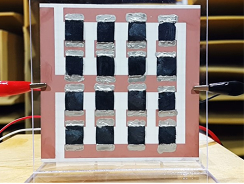
Figure 1: A Thermoacoustic Loudspeaker Consisted of an Array of 16 3D Graphene Aerogels
Figure 2: Two-step Fabrication Process of 3D Reduced Graphene Oxide Aerogel Using Freeze-Drying and Reduction/Doping
Figure 3: X-ray Photoelectron Spectroscopy Graph of the 3D Reduced Graphene Oxide Aerogel and Its Scanning Electron Microscope Image
2016.10.05 View 15310
 -
 Continuous Roll-Process Technology for Transferring and Packaging Flexible Large-Scale Integrated Circuits
A research team led by Professor Keon Jae Lee from KAIST and by Dr. Jae-Hyun Kim from the Korea Institute of Machinery and Materials (KIMM) has jointly developed a continuous roll-processing technology that transfers and packages flexible large-scale integrated circuits (LSI), the key element in constructing the computer’s brain such as CPU, on plastics to realize flexible electronics.
Professor Lee previously demonstrated the silicon-based flexible LSIs using 0.18 CMOS (complementary metal-oxide semiconductor) process in 2013 (ACS Nano, “In Vivo Silicon-based Flexible Radio Frequency Integrated Circuits Monolithically Encapsulated with Biocompatible Liquid Crystal Polymers”) and presented the work in an invited talk of 2015 International Electron Device Meeting (IEDM), the world’s premier semiconductor forum.
Highly productive roll-processing is considered a core technology for accelerating the commercialization of wearable computers using flexible LSI. However, realizing it has been a difficult challenge not only from the roll-based manufacturing perspective but also for creating roll-based packaging for the interconnection of flexible LSI with flexible displays, batteries, and other peripheral devices.
To overcome these challenges, the research team started fabricating NAND flash memories on a silicon wafer using conventional semiconductor processes, and then removed a sacrificial wafer leaving a top hundreds-nanometer-thick circuit layer. Next, they simultaneously transferred and interconnected the ultrathin device on a flexible substrate through the continuous roll-packaging technology using anisotropic conductive film (ACF). The final silicon-based flexible NAND memory successfully demonstrated stable memory operations and interconnections even under severe bending conditions. This roll-based flexible LSI technology can be potentially utilized to produce flexible application processors (AP), high-density memories, and high-speed communication devices for mass manufacture.
Professor Lee said, “Highly productive roll-process was successfully applied to flexible LSIs to continuously transfer and interconnect them onto plastics. For example, we have confirmed the reliable operation of our flexible NAND memory at the circuit level by programming and reading letters in ASCII codes. Out results may open up new opportunities to integrate silicon-based flexible LSIs on plastics with the ACF packing for roll-based manufacturing.”
Dr. Kim added, “We employed the roll-to-plate ACF packaging, which showed outstanding bonding capability for continuous roll-based transfer and excellent flexibility of interconnecting core and peripheral devices. This can be a key process to the new era of flexible computers combining the already developed flexible displays and batteries.”
The team’s results will be published on the front cover of Advanced Materials (August 31, 2016) in an article entitled “Simultaneous Roll Transfer and Interconnection of Silicon NAND Flash Memory.” (DOI: 10.1002/adma.201602339)
YouTube Link: https://www.youtube.com/watch?v=8OJjAEm27sw
Picture 1: This schematic image shows the flexible silicon NAND flash memory produced by the simultaneous roll-transfer and interconnection process.
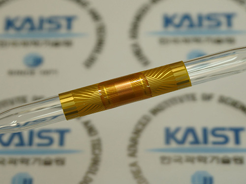
Picture 2: The flexible silicon NAND flash memory is attached to a 7 mm diameter glass rod.
2016.09.01 View 12692
 -
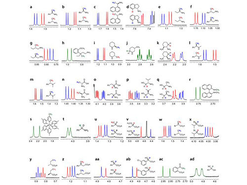 KAIST Develops New Technique for Chiral Activity in Molecules
Professor Hyunwoo Kim of the Chemistry Department and his research team have developed a technique that can easily analyze the optical activity of charged compounds by using nuclear magnetic resonance (NMR) spectroscopy. The research finding entitled “H NMR Chiral Analysis of Charged Molecules via Ion Pairing with Aluminum Complexes” was published online in the October 19th issue of The Journal of the American Chemical Society.
The technique relies on observation of the behavior of optical isomers. Molecules with the same composition that are mirror images of each other are optical isomers. For example, the building blocks of all living organisms, amino acids, are a single optical isomer. In our bodies, optical isomers bring different physiological changes due to their distinct optical activities. Therefore, controlling and analyzing the optical activities are critical when developing a new drug.
High-performance liquid chromatography (HPLC) is the de facto standard of analyzing the optical activity of a compound. However, HPLC is very expensive that many laboratories can’t afford to have. In addition, with the machine, one analysis may take 30 minutes to one hour to complete. It lacks in signal sensitivity and chemical decomposition, and the application is limited to nonpolar compounds.
Usually adopted in analyzing the structure of a chemical compound, NMR spectroscopy requires only one to five minutes per single analysis. Since it is essential for analyzing the molecular structure, many chemistry labs have NMR equipment. However, until this technique was invented, no other research team had reported an effective way of using the NMR spectroscopy to decompose the signal of chiral activity of a compound.
The research team uses negatively-charged metal compounds in NMR spectroscopy. The technique employs negatively-charged metal compounds which bond ionically to positively- and negatively-charged optical compounds. As a result, the NMR spectroscopy can distinguish the signal from chiral activity. Not only can it analyze various chemicals without structural constraints, but it can also be used for both nonpolar and polar solvents.
As many compounds for new drugs have functional groups, which can be charged, this analysis method can be directly employed in the development process of drugs. Professor Kim said, “A revolutionary analysis method has been developed using simple chemical principles. I hope that our method will be applied to the development of new medicine.”
This research was sponsored by the Center for Nanomaterials and Chemical Reactions at the Institute for Basic Science and the Supercomputing Research Center of KAIST.
Picture 1: Separations of NMR Signals of Chemicals due to Interaction with Metal Compounds
Picture 2: Separations of NMR Signals in Different Chemicals
2015.11.20 View 12603
 -
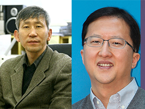 Professors Sukbok Chang and Jang-Wook Choi Receive the 2015 Knowledge Award from the Korean Government
The Ministry of Science, ICT and Future Planning (MISP) of the Republic of Korea announced the 2015 Knowledge Awards on October 20, 2015. Two KAIST professors received the award.
Established in 2009, the awards are presented to Korean scientists whose publications have contributed to the international science community. Specifically, the MISP used the two biggest science databases, Science Citation Index Expanded (SCIE) and Scopus, to identify ten highly cited papers ranked in the top 1% by total citations in the past ten years.
Professor Sukbok Chang of Chemistry (left in the picture below) is a global authority in the field of catalytic hydrocarbon functionalization. His paper entitled “Palladium-catalyzed C-H Functionalization of Pyridine N-Oxides: Highly Selective Alkenylation and Direct Arylation with Unactivated Arenes,” which was published in the Journal of the American Chemical Society in 2008, was once selected by Thomson Reuters as one of the “Most Influential Research Papers of the Month.” In 2011, the American Chemical Society included his paper in the list of the top 20 research papers that were most frequently cited in the last three years.
Professor Jang-Wook Choi of the Graduate School of EEWS (Energy, Environment, Water, and Sustainability) has been known for his leading research in rechargeable battery, supercapacitor, and materials chemistry. In particular, his work on secondary fuel cells attracted significant attention from academia and industry in Korea. Professor Choi developed a super-thin flexible lithium-ion battery this year, thinner than a credit card, which lasts longer than the existing batteries and with greater performance. He also developed new electrode materials for next-generation sodium-ion and magnesium secondary fuel cells.
Professor Sukbok Chang (left) and Professor Jang-Wook Choi (right)
2015.10.23 View 13995
 -
 3D Plasmon Antenna Capable of Focusing Light into Few Nanometers
Professors Myung-Ki Kim and Yong-Hee Lee, both of the Physics Department at KAIST, and their research teams have developed a three dimensional (3D) gap-plasmon antenna which can focus light into a space a few nanometers wide. Their research findings were published in the June 10th issue of Nano Letters.
Focusing light into a point-like space is an active research field with many applications. However, concentrating light into a smaller space than its wavelength is often hindered by diffraction. To tackle this problem, many researchers have utilized the plasmonic phenomenon of a metal where light can be confined to a greater extent by overcoming the diffraction limit.
Many researchers have focused on developing a two dimensional (2D) plasmon antenna and were able to focus a light under 5 nanometers wide. However, this 2D antenna revealed a challenge: the light disperses to the opposite end regardless of how small its beam was focused. To solve this difficulty, a 3D structure had to be employed to maximize the light's intensity.
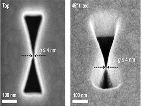
Adopting the proximal focused-ion-beam milling technology, the KAIST research team developed a 3D four nanometer wide gap-plasmon antenna. By squeezing the photons into a 3D nano space of 4 x 10 x 10 nm3 size, the researchers were able to increase the intensity of light by 400,000 times stronger than that of the incident light. Capitalizing on the enhanced intensity of light within the antenna, they intensified the second-harmonic signal and verified that the light was focused in the nano gap by scanning cathodoluminescent images.
The researchers anticipate that this technology will improve the speed of data transfer and processing up to the level of a terahertz (one trillion times per second) and to enlarge the storage volume per unit area on hard disks by 100 times. In addition, high definition images of submolecule size can be taken with actual light, instead of with an electron microscope, while improving the semiconductor process to a smaller size of few nanometers.
Professor Kim said, “A simple yet ingenious idea has shifted the research paradigm from 2D gap-plasmon antennas to 3D antennas. This technology will see numerous applications including in the field of information technology, data storage, imaging medical science, and semiconductor processes.”
The research was sponsored by the National Research Foundation of Korea.
Figure 1: 3D Gap-Plasmon Antenna Structure and Simulation Results
Figure 2 – Constructed 3D Gap-Plasmon Antenna Structure
Figure 3 – Amplified Second Harmonic Signal Generation and Light Focused in the Nano Gap
2015.06.24 View 11046
 -
 KAIST Team Develops Flexible PRAM
Phase change random access memory (PRAM) is one of the strongest candidates for next-generation nonvolatile memory for flexible and wearable electronics. In order to be used as a core memory for flexible devices, the most important issue is reducing high operating current. The effective solution is to decrease cell size in sub-micron region as in commercialized conventional PRAM. However, the scaling to nano-dimension on flexible substrates is extremely difficult due to soft nature and photolithographic limits on plastics, thus practical flexible PRAM has not been realized yet.
Recently, a team led by Professors Keon Jae Lee and Yeon Sik Jung of the Department of Materials Science and Engineering at KAIST has developed the first flexible PRAM enabled by self-assembled block copolymer (BCP) silica nanostructures with an ultralow current operation (below one quarter of conventional PRAM without BCP) on plastic substrates. BCP is the mixture of two different polymer materials, which can easily create self-ordered arrays of sub-20 nm features through simple spin-coating and plasma treatments. BCP silica nanostructures successfully lowered the contact area by localizing the volume change of phase-change materials and thus resulted in significant power reduction. Furthermore, the ultrathin silicon-based diodes were integrated with phase-change memories (PCM) to suppress the inter-cell interference, which demonstrated random access capability for flexible and wearable electronics. Their work was published in the March issue of ACS Nano: "Flexible One Diode-One Phase Change Memory Array Enabled by Block Copolymer Self-Assembly."
Another way to achieve ultralow-powered PRAM is to utilize self-structured conductive filaments (CF) instead of the resistor-type conventional heater. The self-structured CF nanoheater originated from unipolar memristor can generate strong heat toward phase-change materials due to high current density through the nanofilament. This ground-breaking methodology shows that sub-10 nm filament heater, without using expensive and non-compatible nanolithography, achieved nanoscale switching volume of phase change materials, resulted in the PCM writing current of below 20 uA, the lowest value among top-down PCM devices. This achievement was published in the June online issue of ACS Nano: "Self-Structured Conductive Filament Nanoheater for Chalcogenide Phase Transition." In addition, due to self-structured low-power technology compatible to plastics, the research team has recently succeeded in fabricating a flexible PRAM on wearable substrates.
Professor Lee said, "The demonstration of low power PRAM on plastics is one of the most important issues for next-generation wearable and flexible non-volatile memory. Our innovative and simple methodology represents the strong potential for commercializing flexible PRAM."
In addition, he wrote a review paper regarding the nanotechnology-based electronic devices in the June online issue of Advanced Materials entitled "Performance Enhancement of Electronic and Energy Devices via Block Copolymer Self-Assembly."
Picture Caption:
Low-power nonvolatile PRAM for flexible and wearable memories enabled by (a) self-assembled BCP silica nanostructures and (b) self-structured conductive filament nanoheater.
2015.06.15 View 16179
 -
 Anti-Cancer Therapy Delivering Drug to an Entire Tumor Developed
KAIST’s Department of Bio and Brain Engineering Professor Ji-Ho Park and his team successfully developed a new highly efficacious anti-cancer nanotechnology by delivering anti-cancer drugs uniformly to an entire tumor. Their research results were published in Nano Letters online on March 31, 2015.
To treat inoperable tumors, anti-cancer medicine is commonly used. However, efficient drug delivery to tumor cells is often difficult, treating an entire tumor with drugs even more so.
Using the existing drug delivery systems, including nanotechnology, a drug can be delivered only to tumor cells near blood vessels, leaving cells at the heart of a tumor intact. Since most drugs are injected into the bloodstream, tumor recurrence post medication is frequent.
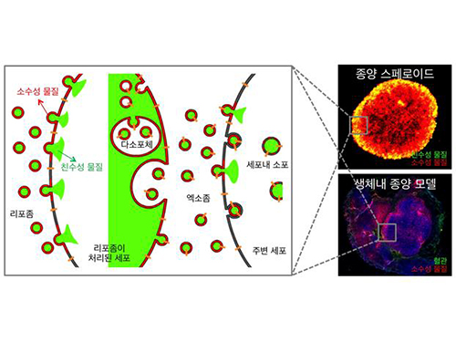
Therefore, the team used liposomes that can fuse to the cell membrane and enter the cell. Once inside liposomes the drug can travel into the bloodstream, enter tumor cells near blood vessels, where they are loaded to exosomes, which are naturally occurring nanoparticles in the body. Since exosomes can travel between cells, the drug can be delivered efficiently into inner cells of the tumor.
Exosomes, which are secreted by cells that exist in the tumor microenvironment, is known to have an important role in tumor progression and metastasis since they transfer biological materials between cells. The research team started the investigation recognizing the possibility of delivering the anti-cancer drug to the entire tumor using exosomes.
The team injected the light-sensitive anti-cancer drug using their new delivery technique into experimental mice. The researchers applied light to the tumor site to activate the anti-cancer treatment and analyzed a tissue sample. They observed the effects of the anti-cancer drug in the entire tumor tissue.
The team’s results establish a ground-breaking foothold in drug delivery technology development that can be tailored to specific diseases by understanding its microenvironment. The work paves the way to more effective drug delivery systems for many chronic diseases, including cancer tumors that were difficult to treat due to the inability to penetrate deep into the tissue.
The team is currently conducting experiments with other anti-cancer drugs, which are being developed by pharmaceutical companies, using their tumor-penetrating drug delivery nanotechnology, to identify its effects on malignant tumors.
Professor Park said, “This research is the first to apply biological nanoparticles, exosomes that are continuously secreted and can transfer materials to neighboring cells, to deliver drugs directly to the heart of tumor.”
Picture: Incorporation of hydrophilic and hydrophobic compounds into membrane vesicles by engineering the parental cells via synthetic liposomes.
2015.04.07 View 12936
 -
 Polymers with Highly Improved Light-transformation Efficiency
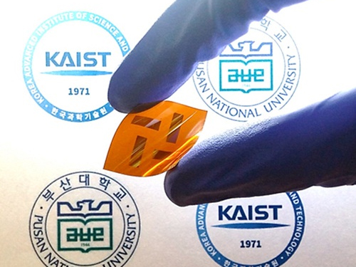
A joint Korean research team, led by Professor Bum-Joon Kim of the Department of Chemical and Biomolecular Engineering at KAIST and Professor Young-Woo Han of the Department of Nanofusion Engineering at Pusan National University, has developed a new type of electrically-conductive polymer for solar batteries with an improved light-transformation efficiency of up to 5%. The team considers it a viable replacement for existing plastic batteries for solar power which is viewed as the energy source of the future.
Polymer solar cells have greater structural stability and heat resistance compared to fullerene organic solar cells. However, they have lower light-transformation efficiency—below 4%—compared to 10% of the latter. The low efficiency is due to the failure of blending among the polymers that compose the active layer of the cell. This phenomenon deters the formation and movement of electrons and thus lowers light-transformation efficiency.
By manipulating the structure and concentration of conductive polymers, the team was able to effectively increase the polymer blending and increase light-transformation efficiency. The team was able to maximize the efficiency up to 6% which is the highest reported ratio.
Professor Kim said, “This research demonstrates that conductive polymer plastics can be used widely for solar cells and batteries for mobile devices.”
The research findings were published in the February 18th issue of the Journal of the American Chemical Society (JACS).
Picture: Flexible Solar Cell Polymer Developed by the Research Team
2015.04.05 View 12178
 -
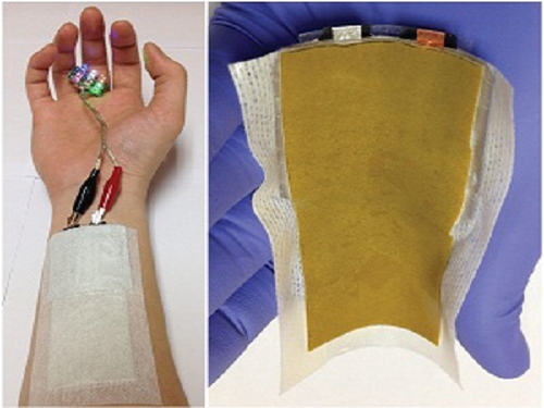 KAIST Develops a Credit-Card-Thick Flexible Lithium Ion Battery
Since the battery can be charged wirelessly, useful applications are expected including medical patches and smart cards.
Professor Jang Wook Choi at KAIST’s Graduate School of Energy, Environment, Water, and Sustainability (EEWS) and Dr. Jae Yong Song at the Korea Research Institute of Standards and Science jointly led research to invent a flexible lithium ion battery that is thinner than a credit card and can be charged wirelessly.
Their research findings were published online in Nano Letters on March 6, 2015. Lithium ion batteries are widely used today in various electronics including mobile devices and electronic cars. Researchers said that their work could help accelerate the development of flexible and wearable electronics.
Conventional lithium ion batteries are manufactured based on a layering technology, stacking up anodes, separating films, and cathodes like a sandwich, which makes it difficult to reduce their thickness. In addition, friction arises between layers, making the batteries impossible to bend. The coating films of electrodes easily come off, which contributes to the batteries’ poor performance.
The research team abandoned the existing production technology. Instead, they removed the separating films, layered the cathodes and anodes collinearly on a plane, and created a partition between electrodes to eliminate potential problems, such as short circuits and voltage dips, commonly present in lithium ion batteries.
After more than five thousand consecutive flexing experiments, the research team confirmed the possibility of a more flexible electrode structure while maintaining the battery performance comparable to the level of current lithium ion batteries.
Flexible batteries can be applied to integrated smart cards, cosmetic and medical patches, and skin adhesive sensors that can control a computer with voice commands or gesture as seen in the movie “Iron Man.”
Moreover, the team has successfully developed wireless-charging technology using electromagnetic induction and solar batteries.
They are currently developing a mass production process to combine this planar battery technology and printing, to ultimately create a new paradigm to print semiconductors and batteries using 3D printers.
Professor Choi said, “This new technology will contribute to diversifying patch functions as it is applicable to power various adhesive medical patches.”
Picture 1: Medical patch (left) and flexible secondary battery (right)
Picture 2: Diagram of flexible battery
Picture 3: Smart card embedding flexible battery
2015.03.24 View 13729
 -
 A KAIST research team developed in vivo flexible large scale integrated circuits
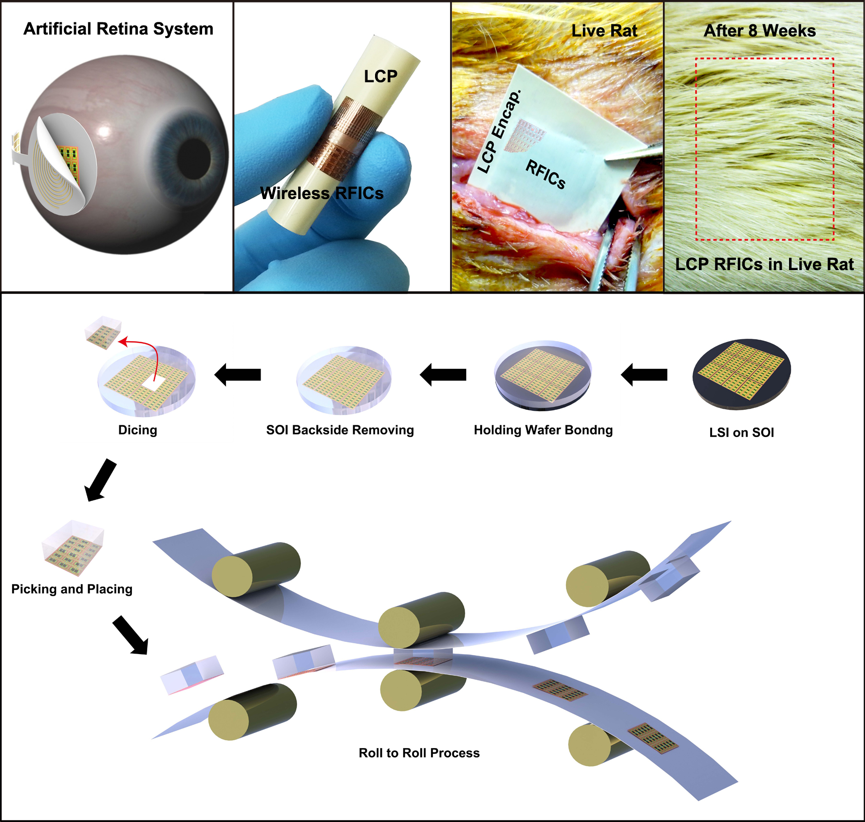
Daejeon, Republic of Korea, May 6th, 2013–-A team led by Professor Keon Jae Lee from the Department of Materials Science and Engineering at KAIST has developed in vivo silicon-based flexible large scale integrated circuits (LSI) for bio-medical wireless communication.
Silicon-based semiconductors have played significant roles in signal processing, nerve stimulation, memory storage, and wireless communication in implantable electronics. However, the rigid and bulky LSI chips have limited uses in in vivo devices due to incongruent contact with the curvilinear surfaces of human organs. Especially, artificial retinas recently approved by the Food and Drug Administration (refer to the press release of FDA"s artificial retina approval) require extremely flexible and slim LSI to incorporate it within the cramped area of the human eye.
Although several research teams have fabricated flexible integrated circuits (ICs, tens of interconnected transistors) on plastics, their inaccurate nano-scale alignment on plastics has restricted the demonstration of flexible nano-transistors and their large scale interconnection for in vivo LSI applications such as main process unit (MPU), high density memory and wireless communication. Professor Lee"s team previously demonstrated fully functional flexible memory using ultrathin silicon membranes (Nano Letters, Flexible Memristive Memory Array on Plastic Substrates), however, its integration level and transistor size (over micron scale) have limited functional applications for flexible consumer electronics.
Professor Keon Jae Lee"s team fabricated radio frequency integrated circuits (RFICs) interconnected with thousand nano-transistors on silicon wafer by state-of-the-art CMOS process, and then they removed the entire bottom substrate except top 100 nm active circuit layer by wet chemical etching. The flexible RF switches for wireless communication were monolithically encapsulated with biocompatible liquid crystal polymers (LCPs) for in vivo bio-medical applications. Finally, they implanted the LCP encapsulated RFICs into live rats to demonstrate the stable operation of flexible devices under in vivo circumstances.
Professor Lee said, "This work could provide an approach to flexible LSI for an ideal artificial retina system and other bio-medical devices. Moreover, the result represents an exciting technology with the strong potential to realize fully flexible consumer electronics such as application processor (AP) for mobile operating system, high-capacity memory, and wireless communication in the near future."
This result was published in the May online issue of the American Chemical Society"s journal, ACS Nano (In vivo Flexible RFICs Monolithically Encapsulated with LCP). They are currently engaged in commercializing efforts of roll-to-roll printing of flexible LSI on large area plastic substrates.
Movie at Youtube Link: Fabrication process for flexible LSI for flexible display, wearable computer and artificial retina for in vivo biomedical application
http://www.youtube.com/watch?v=5PpbM7m2PPs&feature=youtu.be
Applications of in Vivo Flexible Large Scale Integrated Circuits
Top: In vivo flexible large scale integrated circuits (LSI); Bottom: Schematic of roll-to-roll printing of flexible LSI on large area plastics.
2013.06.09 View 15178