photonic
-
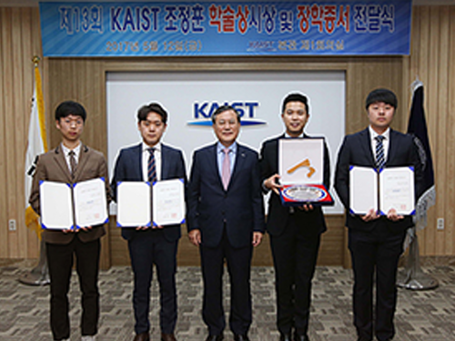 Dr. Zi Jing Wong Named 2017 Jeong Hun Cho Awardee
(Photo caption: The 2017 Jeong Hun Cho Scholarship recipients pose with President Shin (left photo) and Dr. Zi Jing Wong, the recipient of the 2017 Jeong Hun Cho Award)
Dr. Zi Jing Wong, a postdoctoral scholar at the University of California, Berkeley was named the 2017 recipient of the Jeong Hun Cho Award. The award recognizes outstanding young scientists in the field of aerospace engineering annually. The recipient receives a 20 million KRW prize.
The Award Committee said that Dr. Wong who earned his MS at KAIST Department of Aerospace Engineering is a rising scholar in the fields of optic meta materials, photonics, imaging, among others. He has published five papers on the realization of a zero refractive index and the control of a refractive index, as well as the realization of a 3D invisibility cloak in Science and Nature Photonics in 2014 and 2015. Dr. Wong also swept the best paper awards from many international academic societies including the US Materials Research Society, IEEE, SPIE, and Metamaterials Congress in 2015. He finished his Ph.D. at the University of California, Berkeley.
The Award Committee also named three recipients of the Jeong Hun Cho Scholarship: Ph.D. candidate Hyon-Tak Kim of the Department of Aerospace Engineering at KAIST, Ph.D. candidate Ho-Song Park from the Department of Mechanical Engineering at Korea University, and Hyong-Jin Choi of Kongju National University High School.
The award was endowed by the family of the late Ph.D. candidate Jeong Hun Cho who died in a rocket lab accident in the Department of Aerospace Engineering in 2003. Cho was posthumously conferred an honorary doctorate degree.
In memory of Cho, his father established the ‘Jeong Hun Cho Award and Scholarship.’ The scholarship annually selects three young scholars from Cho’s alma maters of KAIST, Korea University, and Kongju National University High School.
2017.05.12 View 13112
 -
 A New Approach to 3D Holographic Displays Greatly Improves the Image Quality
With the addition of holographic diffusers or frosted glasses to wavefront modulators, KAIST researchers offer a simple and practical solution to significantly enhance the performance of 3D dynamic holographic displays by 2,600 times.
The potential applications of three-dimensional (3D) digital holograms are enormous. In addition to arts and entertainment, various fields including biomedical imaging, scientific visualization, engineering design, and displays could benefit from this technology. For example, creating full-sized organs for 3D analysis by doctors could be helpful, but it remained a challenge owing to the limitation of hologram-generation techniques.
A research team led by Professor YongKeun Park of the Physics Department at KAIST has come up with a solution and developed a 3D holographic display that performs more than 2,600 times better than existing 3D holographic displays. This study is expected to improve the limited size and viewing angle of 3D images, which were a major problem of the current holographic displays. The study was published online in Nature Photonics on January 23, 2017.
3D holograms, which often appear in science fiction films, are a familiar technology to the public, but holograms in movies are created with computer graphic effects. Methods for creating true 3D holograms are still being studied in the laboratory. For example, due to the difficulty of generating real 3D images, recent virtual reality (VR) and augmented reality (AR) devices project two different two-dimensional (2D) images onto a viewer to induce optical illusions.
To create a 3D hologram that can be viewed without special equipment such as 3D glasses, the wavefront of light must be controlled using wavefront modulators such as spatial light modulators (SLMs) and deformable mirrors (DMs). A wavefront modulator is an optical manipulation device that can control the direction of light propagation.
However, the biggest limitation to using these modulators as 3D displays is the number of pixels. The large number of pixels that are packed into high-resolution displays developed in recent years are suitable for a 2D image, and the amount of information contained in those pixels cannot produce a 3D image. For this reason, a 3D image that can be made with existing wavefront modulator technology is 1 cm in size with a narrow viewing angle of 3 degrees, which is far from practicable.
As an alternative, KAIST researchers used a DM and added two successive holographic diffusers to scatter light. By scattering light in many directions, this allows for a wider viewing angle and larger image, but results in volume speckle fields, which are caused by the interference of multiple scattered light. Random volume speckle fields cannot be used to display 3D images.
To fix the problem, the researchers employed a wavefront-shaping technique to control the fields. As a result, they succeeded in producing an enhanced 3D holographic image with a viewing angle of 35 degrees in a volume of 2 cm in length, width, and height. This yielded a performance that was about 2,600 times stronger than the original image definition generated when they used a DM without a diffuser.
Professor Park said, “Scattering light has previously been believed to interfere with the recognition of objects, but we have demonstrated that current 3D displays can be improved significantly with an increased viewing angle and image size by properly controlling the scattered light.”
Hyeonseung Yu, who is the lead author of this research article and a doctoral candidate in the Department of Physics, KAIST, noted that this technology signals a good start to develop a practical model for dynamic 3D hologram displays that can be enjoyed without the need for special eyeglasses. “This approach can also be applied to AR and VR technology to enhance the image resolution and viewing angles,” added Yu.
The research paper is entitled “Ultrahigh-definition Dynamic 3D Holographic Display by Active Control of Volume Speckle Fields.”
Figure 1. Concept of Scattering Display
The size and viewing angle of 3D images can be simultaneously increased when a scattering medium (diffuser) is introduced. By controlling the wavefront impinging on the scattering medium, the desired 3D hologram is generated.
Figure 2. Experimental Setup
The optical set-up consists of a deformable mirror and the scattering medium with two successive holographic diffusers. A high-numerical-aperture imaging unit mounted on a three-axis motorized translational system is utilized for wavefront optimization and imaging.
Figure 3. 3D Images Projected
This picture shows 3D images in a volume of 2 cm × 2 cm × 2 cm with a viewing angle of 35 degrees using one of the wavefront modulators, a digital micromirror device (DMD).
Figure 4. Artist’s Rendition of the Proposed Concept
A dynamic 3D hologram of a face is displayed.
2017.02.01 View 14506
 -
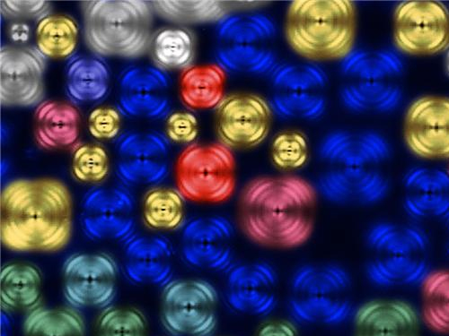 Dr. Se-Jung Kim Receives the Grand Prize at the International Photo and Image Contest on Light
Dr. Se-Jung Kim of the Physics Department at KAIST received the Grand Prize at the 2015 Photo and Image Contest of the International Year of Light and Light-based Technologies.
The United Nations has designated the year 2015 as the International Year of Light and Light-based Technologies.
The Optical Society of Korea celebrated the UN’s designation by hosting an international photo and image contest on the theme of light and optics related technology.
Dr. Kim presented a photo of images taken from a liquid crystal, which was entitled “A Micro Pinwheel.” She took pictures of liquid crystal images with a polarizing microscope and then colored the pictures. The liquid crystal has self-assembled circle domain structures, and each domain can form vortex optics. Her adviser for the project is Professor Yong-Hoon Cho of the Physics Department.
Her work was exhibited during the annual conference of the Optical Society of Korea, which was held on July 13-15, 2015 at Gyeong-Ju Hwabaek International Convention Center. It will also be exhibited at the National Science Museum in Gwacheon and the Kim Dae-Jung Convention Center in Gwangju.
Picture: A Micro Pinwheel
2015.07.31 View 12148
 -
 Professor Kyoungsik Yu Receives the Young IT Engineer Award from IEEE and IEIE of Korea
Professor Kyoungsik Yu of KAIST’s Department of Electrical Engineering is the recipient of this year’s Young IT (Information Technology) Engineer Award that was co-hosted by the Institute of Electrical and Electronics Engineers (IEEE), the Institute of Electronics Engineers of Korea (IEIE), and Haedong Science Culture Foundation in Korea. The award was presented on June 22, 2015 at The Ramada Plaza Jeju Hotel on Jeju Island, Korea.
The Young IT Engineer Award is given to emerging scientists who have made significant contributions to the advancement of technology, society, environment, and creative education.
Professor Yu's main research interests are IT, energy, and imaging through miniaturization and integration of optoelectronic devices. His contribution to academic and technological development is reflected in his publication of more than 100 papers in international journals and conferences, which were cited over 2,200 times.
Professor Yu said, “I’m honored to receive this award and am encouraged by it. I also find the award meaningful because the United Nations has designated this year as the “International Year of Light and Light-based Technologies,” the field I have been involved in as a researcher.”
In addition to Korea, the IEEE has jointly hosted and presented this award to researchers in countries such as Chile, Ecuador, Peru, Singapore, and Italy.
2015.06.22 View 14272
 -
 Extracting Light from Graphite: Core Technology of Graphene Quantum Dots Display Developed
Professor Seokwoo Jeon of the Department of Materials Science and Engineering, Professor Yong-Hoon Cho of the Department of Physics, and Professor Seunghyup Yoo of the Department of Electrical Engineering announced that they were able to develop topnotch graphene quantum dots from graphite.
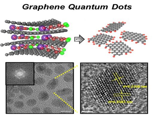
Using the method of synthesizing graphite intercalation compound from graphite with salt and water, the research team developed graphene quantum dots in an ecofriendly way.
The quantum dots have a diameter of 5 nanometers with their sizes equal and yield high quantum efficiency. Unlike conventional quantum dots, they are not comprised of toxic materials such as lead or cadmium. As the quantum dots can be developed from materials which can be easily found in the nature, researchers look forward to putting these into mass production at low cost.
The research team also discovered a luminescence mechanism of graphene quantum dots and confirmed the possibility of commercial use by developing quantum dot light-emitting diodes with brightness of 1,000 cd/m2, which is greater than that of cellphone displays.
Professor Seokwoo Jeon said, “Although quantum dot LEDs have a lower luminous efficiency than existing ones, their luminescent property can be further improved” and emphasized that “using quantum dot displays will allow us to develop not only paper-thin displays but also flexible ones.”
Sponsored by Graphene Research Center in KAIST Institute for NanoCentury, the research finding was published online in the April 20th issue of Advanced Optical Materials.
Picture 1: Graphene quantum dots and their synthesis
Picture 2: Luminescence mechanism of graphene quantum dots
Picture 3: Structure of graphene quantum dots LED and its emission
2014.09.06 View 20027
 -
 The First Demonstration of a Self-powered Cardiac Pacemaker
As the number of pacemakers implanted each year reaches into the millions worldwide, improving the lifespan of pacemaker batteries has been of great concern for developers and manufacturers. Currently, pacemaker batteries last seven years on average, requiring frequent replacements, which may pose patients to a potential risk involved in medical procedures.
A research team from the Korea Advanced Institute of Science and Technology (KAIST), headed by Professor Keon Jae Lee of the Department of Materials Science and Engineering at KAIST and Professor Boyoung Joung, M.D. of the Division of Cardiology at Severance Hospital of Yonsei University, has developed a self-powered artificial cardiac pacemaker that is operated semi-permanently by a flexible piezoelectric nanogenerator.
The artificial cardiac pacemaker is widely acknowledged as medical equipment that is integrated into the human body to regulate the heartbeats through electrical stimulation to contract the cardiac muscles of people who suffer from arrhythmia. However, repeated surgeries to replace pacemaker batteries have exposed elderly patients to health risks such as infections or severe bleeding during operations.
The team’s newly designed flexible piezoelectric nanogenerator directly stimulated a living rat’s heart using electrical energy converted from the small body movements of the rat. This technology could facilitate the use of self-powered flexible energy harvesters, not only prolonging the lifetime of cardiac pacemakers but also realizing real-time heart monitoring.
The research team fabricated high-performance flexible nanogenerators utilizing a bulk single-crystal PMN-PT thin film (iBULe Photonics). The harvested energy reached up to 8.2 V and 0.22 mA by bending and pushing motions, which were high enough values to directly stimulate the rat’s heart.
Professor Keon Jae Lee said:
“For clinical purposes, the current achievement will benefit the development of self-powered cardiac pacemakers as well as prevent heart attacks via the real-time diagnosis of heart arrhythmia. In addition, the flexible piezoelectric nanogenerator could also be utilized as an electrical source for various implantable medical devices.”
This research result was described in the April online issue of Advanced Materials (“Self-Powered Cardiac Pacemaker Enabled by Flexible Single Crystalline PMN-PT Piezoelectric Energy Harvester”: http://onlinelibrary.wiley.com/doi/10.1002/adma.201400562/abstract).
Youtube link: http://www.youtube.com/watch?v=ZWYT2cU_Mog&feature=youtu.be
Picture Caption: A self-powered cardiac pacemaker is enabled by a flexible piezoelectric energy harvester.
2014.06.25 View 18193
 -
 SPIE (The International Society for Optics and Photonics): Scattering Super-lens
The International Society for Optics and Photonics (SPIE), dedicated to advancing an interdisciplinary approach to the science and application of light, published online a short paper authored by a KAIST research team, Dr. Jung-Hoon Park and Professor YongKeun Park of Physics, introducing a new optical technology to observe sub-wavelength light by exploiting multiple light scattering in complex media.
For the article, please go to the link below:
SPIE: Nanotechnology
May 7th, 2014
"Scattering superlens" by Jung-Hoon Park and YongKeun Park
http://spie.org/x108298.xml
2014.05.14 View 8347
 -
 Clear Display Technology Under Sunlight Developed
The late Professor Seung-Man Yang
The last paper of the late Professor Seung-Man Yang, who was a past master of colloids and fluid mechanics
Practical patterning technology of the next generation optical materials, photonic crystals
The mineral opal does not possess any pigments, but it appears colorful to our eyes. This is because only a particular wavelength is reflected due to the regular nano-structure of its surface. The material that causes selective reflection of the light is called photonic crystals.
The deceased Professor Seung-Man Yang and his research team from KAIST’s Chemical and Biomolecular Engineering Department ha ve developed micro-pattern technology using photolithographic process. This can accelerate the commercialization of photonic crystals, which is hailed as the next generation optics material.
The research results were published in the April 16th edition of Advanced Materials, known as the most prestigious world-renowned journal in the field of materials science.
The newly developed photonic crystal micro-pattern could be used as a core material for the next generation reflective display that is clearly visible even under sunlight. Since it does not require a separate light source, a single charge is enough to last for several days.
Until now, many scientists have endeavored to make photonic crystals artificially, however, most were produced in a lump and therefore lacked efficiency. Also, the low mechanical stability of the formed structure prevented from commercialization.
In order to solve these problems, the research team has copied the nano-structure of opals.
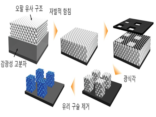
Glass beads were arranged in the same nano-structure as the opal on top of the photoresist material undergoing photocuring by ultraviolet light. The glass beads were installed in the photoresist materials, and UV light was selectively exposed on micro regions. The remaining region was developed by photolithographic process to successfully produce photonic crystals in micro-patterns.
The co-author of the research, KAIST Chemical and Biomolecular Engineering Department’s Professor Sin-Hyeon Kim, said, “Combining the semiconductor process technology with photonic crystal pattern technology can secure the practical applications for photonic crystals.”He also predicted “This technology can be used as the key optical material that configures the next generation reflective color display device with very low power consumption.”
The late Professor Seung-Man Yang was a world-renowned expert in the field of colloids and fluid mechanics. Professor Yang published over 193 papers in international journals and continued his research until his passing in last September.
He received Du Pont Science and Technology Award in 2007, KAIST Person of the Year 2008, Gyeong-Am Academy Award in 2009, as well as the President’s Award of the Republic of Korea in March 2014. The researchers devoted the achievement of this year’s research to Professor Yang in his honor.
Research was conducted by KAIST Photonic-fluidic Integrated Devices Research Team, as a part of the Creative Research Program funded by the Ministry of Science, ICT and Future Planning, Republic of Korea.
Figure 1. Opal [left] and the nano glass bead arrangement structure within the opal [right]
Figure 2. Process chart of the photonic crystal micro-pattern formation based on photolithography
Figure 3. Opal structure [left] and inverted structure of the opal [right]
Figure 4. Photonic crystal micro-pattern in solid colors
Figure 5. Photonic crystal micro-pattern that reflects two different crystals (Red, Green) [left] and pixelated pattern of photonic crystal in three primary colors (Red, Green, Blue) [right] that is applicable to reflective displays
2014.05.14 View 14175
 -
 The First Winner of Sang Soo Lee Award in Optics and Photonics
The Optical Society of Korea and the Optical Society of America selected Mario Garavaglia, a researcher at the La Plata Optical Research Center in Argentina, as the first winner of the Sang Soo Lee Award.
Dr. Garavaglia has been selected to receive the award in recognition for his research and education in the field of optics and photonics in Argentina.
The Sang Soo Lee Award, co-established by the Optical Society of Korea and the Optical Society of America in 2012, is awarded to an individual who has made a significant impact in the field. Special considerations are made for individuals who have introduced a new field of research, helped establish a new industry, or made a great contribution to education in the field.
The award is sponsored by the late Doctor Sang Soo Lee's family, the Optical Society of Korea, and the Optical Society of America.
The late Doctor Sang Soo Lee (1925~2010) has been widely known as the 'father of optics' in Korea. He was an active educator, researcher, and writer. Dr. Lee served as the first director of the Korea Advanced Institute of Science (KAIS), the predecessor to KAIST, which was Korea's first research oriented university.
Dr. Lee also served as the 6th president of KAIST between 1989 to 1991 and was a KAIST professor of physics for 21 years. He oversaw the completion of 50 Ph.D. and 100 Master's students as well as published 230 research papers.
Philip Bucksbaum, the president of the Optical Society of America, commented,
"Garavaglia has been an example to the spirit of the Sang Soo Lee Award. The award is the recognition for his tireless efforts and commitment to the development of optics and photonics in Argentina through his teaching, research, and publications."
Jeong-Won Woo, the president of the Optical Society of Korea, said,
"The Sang Soo Lee Award is given to researchers who have consistently contributed to the development of the field. Garavaglia is a well respected researcher in Argentina, and we are truly happy with his selection."
Dr. Garavaglia established a spectroscopy, optic, and laser laboratory in Universidad Nacional de La Plata in 1966. He founded the Center for Optical Research in 1977 and served as the chief of the laboratory until 1991.
Dr. Garavaglia published over 250 research papers in the fields of classical optics, modern optics, photoemission spectroscopy, and laser spectroscopy. He has also received the Galileo Galilei Award from the International Commission for Optics in 1999.
2014.03.31 View 12052
 -
 Phys.org: Researchers develop non-iridescent, structural, full-spectrum pigments for reflective displays
The latest research work by Professor Shin-Hyun Kim of Chemical and Biomolecular Engineering at KAIST on the “microcapsulation og photonic crystals using osmotic pressure” has been published by Phys.org, a leading web-based science, research and technology news. For the articles, please click the link below:February 20, 2014Researchers develop non-iridescent, structural, full-spectrum pigments for reflective displayshttp://phys.org/news/2014-02-non-iridescent-full-spectrum-pigments.html
2014.02.21 View 9272
 -
 Nature Photonics, a peer-reviewed scientific journal, released a paper written by a KAIST research team on the time-of-flight measurement.
Professor Seung-Woo Kim of the Mechanical Engineering Department, KAIST, and his research team published the result of their study on the measurement of 1 nanometer (nm) precision.
“The time-of-flight of light pulses has long been used as a direct measure of distance, but state-of-the-art measurement precision using conventional light pulses or microwaves peaks at only several hundreds of micrometers. Here, we improve the time-of-flight precision to the nanometer regime by timing femtosecond pulses through phase-locking control of the pulse repetition rate using the optical cross-correlation technique,” Professor Kim said.
According to the experiment conducted by the research team, “An Allan deviation of 117 nm in measuring a 700m distance in air at a sampling rate of 5 millisecond (ms) once the pulse repetition is phased-locked, which reduces to 7 nm as the averaging time increases to 1 second (s).”
When measuring an object located in a far distance, a laser beam is projected to the object, and the reflected light is analyzed; the light is then converted into an electric signal to calculate the distance. In so doing, Professor Kim said, the conventional method of measurement creates at least 1 mm of deviation.
He argues, “This enhanced capability is maintained at long range without periodic ambiguity, and is well suited to lidar applications. This method could also be applied to future space missions involving formation-flying satellites for synthetic aperture imaging and remote experiments related to general relativity theory."
Nature Photonics published the article online on August 8, 2010.
2010.08.18 View 14419
 -
 Photonic crystals allow the fabrication of miniaturized spectrometers
By Courtesy of Nanowerk
Photonic crystals allow the fabrication of miniaturized spectrometers
(Nanowerk Spotlight) Spectrometers are used in materials analysis by measuring the absorption of light by a surface or chemical substance. These instruments measure properties of light over a specific portion of the electromagnetic spectrum. In conventional spectrometers, a diffraction grating splits the light source into several beams with different propagation directions according to the wavelength of the light. Thus, to achieve sufficient spatial separation for intensity measurements at a small slit, a long light path – i.e., a large instrument – is required.
However, for lab-on-a-chip or microTAS (total analysis system) applications, the spectrometer must be integrated into a sub-centimeter scale device to produce a stand-alone platform. To achieve this, researchers at the Korea Advanced Institute of Science and Technology (KAIST) propose a new paradigm in which the spectrometer is based on an array of photonic crystals with different bandgaps.
"Because photonic crystals refelct light of different wavelengths selectively depending on their bandgaps, we can generate reflected light spanning the entire wavelength range for analysis at different spatial positions using patterned photonic crystals," Seung-Man Yang, Director of the National Creative Research Initiative Center for Intergrated Optofluidic Systems and Professor of the Department of Chemical & Biomolecular Engineering at KAIST, tells Nanowerk. "Therefore, when the light source impinges on the patterned photonic crytals, we can construct the spectrum using the reflection intensity profile from the constituent photonic crystals."
Photonic crystals – also known as photonic band gap material – are similar to semiconductors, only that the electrons are replaced by photons (i.e. light). By creating periodic structures out of materials with contrast in their dielectric constants, it becomes possible to guide the flow of light through the photonic crystals in a way similar to how electrons are directed through doped regions of semiconductors. The photonic band gap (that forbids propagation of a certain frequency range of light) gives rise to distinct optical phenomena and enables one to control light with amazing facility and produce effects that are impossible with conventional optics.
To demonstrate this new concept based on patterned photonic crystals, Yang and his group used non-close-packed colloidal crystals of silica particles dispersed in photocurable resin. Due to the repulsive interparticle potential, monodisperse silica particles spontaneously crystallize into non-close-packed face-centered cubic (fcc) structures at volume fractions above 0.1. Therefore, the particle volume fraction determines both the lattice constant and the bandgap position.
a) Optical image of an ETPTA film containing porous photonic crystal stripe patterns with 20 different bandgaps. b) Reflectance spectra from the 20 strips. c) Optical microscope image of the middle region with the parallel stripe pattern (denoted as white-dotted box in a). d) Cross-sectional SEM images of first, sixth, eleventh and seventeenth strips. The scale bars in a, c and d are 1 cm, 2mm and 2 µm, respectively. (reprinted with permission from Wiley-VCH Verlag)
Reporting their findings in a recent issue of Advanced Materials ("Integration of Colloidal Photonic Crystals toward Miniaturized Spectrometers"), the KAIST team has demonstrated the integration of colloidal photonic crystals with 20 different bandgaps into freestanding films (prepared by soft lithography), and their application as a spectrometer.
Yang explains that the team was able to precisely control the photonic bandgap by varying the particle size and volume fration.
"The prepared colloidal composite structures showed high physical rigidity and chemical resistivity" he says. "The composite structure is suitable for spectroscopic use due to the small full widths at half maximum (FWHMs) of the reflectance spectra, which mean that there is little overlap of the reflectance spectra of neighboring photonic crystal strips."
"On the other hand" says Yang, "porous photonic crystals showed large FWHMs and high reflectivities, which should prove useful in many practical photonic applications that require high optical performance and physical rigidity as well as simple and inexpensive preparation."
In addition to fabricating miniaturized spectrometers, which can for instance be integrated into small lab-on-a-chip devices, these integrated photonic crystals can be potentially used for tunable band reflection mirrors, optical switches, and tunable lasing cavities. Moreover, patterned photonic crystals with RGB colors are well-suited for use in reflection-mode microdisplay devices.
Yang points out that, although the spectrometric resolution can be reduced by employing the smaller bandgap interval and photonic bandwidth, there is a limitation. "Now, we are studying photonic crystals with continuous modulation of bandgap position. We expect that the photonic crystals can reduce the resolution to 0.01 nm."
By Michael Berger. Copyright 2010 Nanowerk
2010.03.17 View 16118
Photonic crystals allow the fabrication of miniaturized spectrometers
By Courtesy of Nanowerk
Photonic crystals allow the fabrication of miniaturized spectrometers
(Nanowerk Spotlight) Spectrometers are used in materials analysis by measuring the absorption of light by a surface or chemical substance. These instruments measure properties of light over a specific portion of the electromagnetic spectrum. In conventional spectrometers, a diffraction grating splits the light source into several beams with different propagation directions according to the wavelength of the light. Thus, to achieve sufficient spatial separation for intensity measurements at a small slit, a long light path – i.e., a large instrument – is required.
However, for lab-on-a-chip or microTAS (total analysis system) applications, the spectrometer must be integrated into a sub-centimeter scale device to produce a stand-alone platform. To achieve this, researchers at the Korea Advanced Institute of Science and Technology (KAIST) propose a new paradigm in which the spectrometer is based on an array of photonic crystals with different bandgaps.
"Because photonic crystals refelct light of different wavelengths selectively depending on their bandgaps, we can generate reflected light spanning the entire wavelength range for analysis at different spatial positions using patterned photonic crystals," Seung-Man Yang, Director of the National Creative Research Initiative Center for Intergrated Optofluidic Systems and Professor of the Department of Chemical & Biomolecular Engineering at KAIST, tells Nanowerk. "Therefore, when the light source impinges on the patterned photonic crytals, we can construct the spectrum using the reflection intensity profile from the constituent photonic crystals."
Photonic crystals – also known as photonic band gap material – are similar to semiconductors, only that the electrons are replaced by photons (i.e. light). By creating periodic structures out of materials with contrast in their dielectric constants, it becomes possible to guide the flow of light through the photonic crystals in a way similar to how electrons are directed through doped regions of semiconductors. The photonic band gap (that forbids propagation of a certain frequency range of light) gives rise to distinct optical phenomena and enables one to control light with amazing facility and produce effects that are impossible with conventional optics.
To demonstrate this new concept based on patterned photonic crystals, Yang and his group used non-close-packed colloidal crystals of silica particles dispersed in photocurable resin. Due to the repulsive interparticle potential, monodisperse silica particles spontaneously crystallize into non-close-packed face-centered cubic (fcc) structures at volume fractions above 0.1. Therefore, the particle volume fraction determines both the lattice constant and the bandgap position.
a) Optical image of an ETPTA film containing porous photonic crystal stripe patterns with 20 different bandgaps. b) Reflectance spectra from the 20 strips. c) Optical microscope image of the middle region with the parallel stripe pattern (denoted as white-dotted box in a). d) Cross-sectional SEM images of first, sixth, eleventh and seventeenth strips. The scale bars in a, c and d are 1 cm, 2mm and 2 µm, respectively. (reprinted with permission from Wiley-VCH Verlag)
Reporting their findings in a recent issue of Advanced Materials ("Integration of Colloidal Photonic Crystals toward Miniaturized Spectrometers"), the KAIST team has demonstrated the integration of colloidal photonic crystals with 20 different bandgaps into freestanding films (prepared by soft lithography), and their application as a spectrometer.
Yang explains that the team was able to precisely control the photonic bandgap by varying the particle size and volume fration.
"The prepared colloidal composite structures showed high physical rigidity and chemical resistivity" he says. "The composite structure is suitable for spectroscopic use due to the small full widths at half maximum (FWHMs) of the reflectance spectra, which mean that there is little overlap of the reflectance spectra of neighboring photonic crystal strips."
"On the other hand" says Yang, "porous photonic crystals showed large FWHMs and high reflectivities, which should prove useful in many practical photonic applications that require high optical performance and physical rigidity as well as simple and inexpensive preparation."
In addition to fabricating miniaturized spectrometers, which can for instance be integrated into small lab-on-a-chip devices, these integrated photonic crystals can be potentially used for tunable band reflection mirrors, optical switches, and tunable lasing cavities. Moreover, patterned photonic crystals with RGB colors are well-suited for use in reflection-mode microdisplay devices.
Yang points out that, although the spectrometric resolution can be reduced by employing the smaller bandgap interval and photonic bandwidth, there is a limitation. "Now, we are studying photonic crystals with continuous modulation of bandgap position. We expect that the photonic crystals can reduce the resolution to 0.01 nm."
By Michael Berger. Copyright 2010 Nanowerk
2010.03.17 View 16118