Semiconductor
-
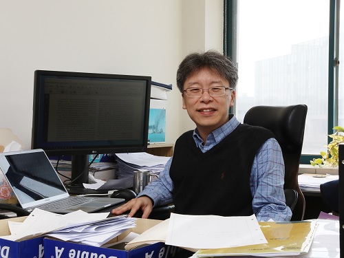 Professor Heung-Sun Sim the MSIT Scientist of July
Professor Heung-Sun Sim from the Department of Physics was selected as the Scientist of July by the Ministry of Science and ICT. Professor Sim was recognized for his research of the Kondo effect, which opened a novel way to engineer spin screening and entanglement by directly observing a quantum phenomenon known as a Kondo screening cloud. His research revealed that the cloud can mediate interactions between distant spins confined in quantum dots, which is a necessary protocol for semiconductor spin-based quantum information processing. This phenomenon is essentially a cloud that masks magnetic impurities in a material. It was known to exist but its spatial extension had never been observed, creating controversy over whether such an extension actually existed. The research was reported in Nature in March 2020. With this award, Professor Sim received 10 million KRW in prize money.
2021.07.12 View 7217
 -
 Quantum Laser Turns Energy Loss into Gain
A new laser that generates quantum particles can recycle lost energy for highly efficient, low threshold laser applications
Scientists at KAIST have fabricated a laser system that generates highly interactive quantum particles at room temperature. Their findings, published in the journal Nature Photonics, could lead to a single microcavity laser system that requires lower threshold energy as its energy loss increases.
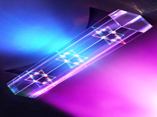
The system, developed by KAIST physicist Yong-Hoon Cho and colleagues, involves shining light through a single hexagonal-shaped microcavity treated with a loss-modulated silicon nitride substrate. The system design leads to the generation of a polariton laser at room temperature, which is exciting because this usually requires cryogenic temperatures.
The researchers found another unique and counter-intuitive feature of this design. Normally, energy is lost during laser operation. But in this system, as energy loss increased, the amount of energy needed to induce lasing decreased. Exploiting this phenomenon could lead to the development of high efficiency, low threshold lasers for future quantum optical devices.
“This system applies a concept of quantum physics known as parity-time reversal symmetry,” explains Professor Cho. “This is an important platform that allows energy loss to be used as gain. It can be used to reduce laser threshold energy for classical optical devices and sensors, as well as quantum devices and controlling the direction of light.”
The key is the design and materials. The hexagonal microcavity divides light particles into two different modes: one that passes through the upward-facing triangle of the hexagon and another that passes through its downward-facing triangle. Both modes of light particles have the same energy and path but don’t interact with each other.
However, the light particles do interact with other particles called excitons, provided by the hexagonal microcavity, which is made of semiconductors. This interaction leads to the generation of new quantum particles called polaritons that then interact with each other to generate the polariton laser. By controlling the degree of loss between the microcavity and the semiconductor substrate, an intriguing phenomenon arises, with the threshold energy becoming smaller as energy loss increases. This research was supported by the Samsung Science and Technology Foundation and Korea’s National Research Foundation.
-PublicationSong,H.G, Choi, M, Woo, K.Y. Yong-Hoon Cho Room-temperature polaritonic non-Hermitian system with single microcavityNature Photonics (https://doi.org/10.1038/s41566-021-00820-z)
-ProfileProfessor Yong-Hoon ChoQuantum & Nanobio Photonics Laboratoryhttp://qnp.kaist.ac.kr/
Department of PhysicsKAIST
2021.07.07 View 9826
 -
 Scientists Observe the Elusive Kondo Screening Cloud
Scientists ended a 50-year quest by directly observing a quantum phenomenon
An international research group of Professor Heung-Sun Sim has ended a 50-year quest by directly observing a quantum phenomenon known as a Kondo screening cloud. This research, published in Nature on March 11, opens a novel way to engineer spin screening and entanglement. According to the research, the cloud can mediate interactions between distant spins confined in quantum dots, which is a necessary protocol for semiconductor spin-based quantum information processing. This spin-spin interaction mediated by the Kondo cloud is unique since both its strength and sign (two spins favor either parallel or anti-parallel configuration) are electrically tunable, while conventional schemes cannot reverse the sign.
This phenomenon, which is important for many physical phenomena such as dilute magnetic impurities and spin glasses, is essentially a cloud that masks magnetic impurities in a material. It was known to exist but its spatial extension had never been observed, creating controversy over whether such an extension actually existed.
Magnetism arises from a property of electrons known as spin, meaning that they have angular momentum aligned in one of either two directions, conventionally known as up and down. However, due to a phenomenon known as the Kondo effect, the spins of conduction electrons—the electrons that flow freely in a material—become entangled with a localized magnetic impurity, and effectively screen it. The strength of this spin coupling, calibrated as a temperature, is known as the Kondo temperature.
The size of the cloud is another important parameter for a material containing multiple magnetic impurities because the spins in the cloud couple with one another and mediate the coupling between magnetic impurities when the clouds overlap. This happens in various materials such as Kondo lattices, spin glasses, and high temperature superconductors.
Although the Kondo effect for a single magnetic impurity is now a text-book subject in many-body physics, detection of its key object, the Kondo cloud and its length, has remained elusive despite many attempts during the past five decades. Experiments using nuclear magnetic resonance or scanning tunneling microscopy, two common methods for understanding the structure of matter, have either shown no signature of the cloud, or demonstrated a signature only at a very short distance, less than 1 nanometer, so much shorter than the predicted cloud size, which was in the micron range.
In the present study, the authors observed a Kondo screening cloud formed by an impurity defined as a localized electron spin in a quantum dot—a type of “artificial atom”—coupled to quasi-one-dimensional conduction electrons, and then used an interferometer to measure changes in the Kondo temperature, allowing them to investigate the presence of a cloud at the interferometer end.
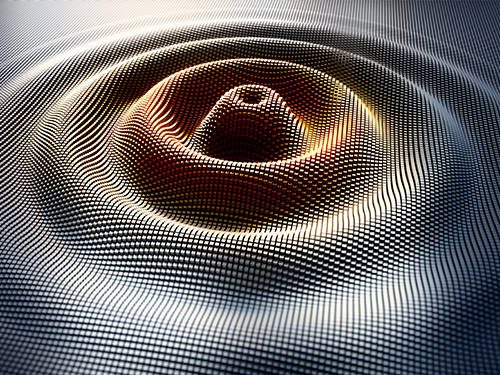
Essentially, they slightly perturbed the conduction electrons at a location away from the quantum dot using an electrostatic gate. The wave of conducting electrons scattered by this perturbation returned back to the quantum dot and interfered with itself. This is similar to how a wave on a water surface being scattered by a wall forms a stripe pattern. The Kondo cloud is a quantum mechanical object which acts to preserve the wave nature of electrons inside the cloud.
Even though there is no direct electrostatic influence of the perturbation on the quantum dot, this interference modifies the Kondo signature measured by electron conductance through the quantum dot if the perturbation is present inside the cloud. In the study, the researchers found that the length as well as the shape of the cloud is universally scaled by the inverse of the Kondo temperature, and that the cloud’s size and shape were in good agreement with theoretical calculations.
Professor Sim at the Department of Physics proposed the method for detecting the Kondo cloud in the co-research with the RIKEN Center for Emergent Matter Science, the City University of Hong Kong, the University of Tokyo, and Ruhr University Bochum in Germany.
Professor Sim said, “The observed spin cloud is a micrometer-size object that has quantum mechanical wave nature and entanglement. This is why the spin cloud has not been observed despite a long search. It is remarkable in a fundamental and technical point of view that such a large quantum object can now be created, controlled, and detected.
Dr. Michihisa Yamamoto of the RIKEN Center for Emergent Matter Science also said, “It is very satisfying to have been able to obtain real space image of the Kondo cloud, as it is a real breakthrough for understanding various systems containing multiple magnetic impurities. The size of the Kondo cloud in semiconductors was found to be much larger than the typical size of semiconductor devices.”
Publication:
Borzenets et al. (2020) Observation of the Kondo screening cloud. Nature, 579. pp.210-213. Available online at https://doi.org/10.1038/s41586-020-2058-6
Profile:
Heung-Sun Sim, PhD
Professor
hssim@kaist.ac.kr
https://qet.kaist.ac.kr/
Quantum Electron Correlation & Transport Theory Group (QECT Lab)
https://qc.kaist.ac.kr/index.php/group1/
Center for Quantum Coherence In COndensed Matter
Department of Physics
https://www.kaist.ac.kr
Korea Advanced Institute of Science and Technology (KAIST)
Daejeon, Republic of Korea
2020.03.13 View 15329
 -
 Black Phosphorous Tunnel Field-Effect Transistor as an Alternative Ultra-low Power Switch
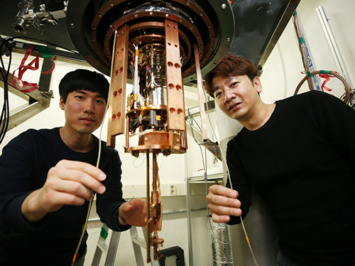
Researchers have reported a black phosphorus transistor that can be used as an alternative ultra-low power switch. A research team led by Professor Sungjae Cho in the KAIST Department of Physics developed a thickness-controlled black phosphorous tunnel field-effect transistor (TFET) that shows 10-times lower switching power consumption as well as 10,000-times lower standby power consumption than conventional complementary metal-oxide-semiconductor (CMOS) transistors.
The research team said they developed fast and low-power transistors that can replace conventional CMOS transistors. In particular, they solved problems that have degraded TFET operation speed and performance, paving the way to extend Moore’s Law.
In the study featured in Nature Nanotechnology last month, Professor Cho’s team reported a natural heterojunction TFET with spatially varying layer thickness in black phosphorous without interface problems. They achieved record-low average subthreshold swing values over 4-5 dec of current and record-high, on-state current, which allows the TFETs to operate as fast as conventional CMOS transistors with as much lower power consumption.
"We successfully developed the first transistor that achieved the essential criteria for fast, low-power switching. Our newly developed TFETs can replace CMOS transistors by solving a major issue regarding the performance degradation of TFETs,"Professor Cho said.
The continuous down-scaling of transistors has been the key to the successful development of current information technology. However, with Moore’s Law reaching its limits due to the increased power consumption, the development of new alternative transistor designs has emerged as an urgent need.
Reducing both switching and standby power consumption while further scaling transistors requires overcoming the thermionic limit of subthreshold swing, which is defined as the required voltage per ten-fold current increase in the subthreshold region. In order to reduce both the switching and standby power of CMOS circuits, it is critical to reduce the subthreshold swing of the transistors.
However, there is fundamental subthreshold swing limit of 60 mV/dec in CMOS transistors, which originates from thermal carrier injection. The International Roadmap for Devices and Systems has already predicted that new device geometries with new materials beyond CMOS will be required to address transistor scaling challenges in the near future. In particular, TFETs have been suggested as a major alternative to CMOS transistors, since the subthreshold swing in TFETs can be substantially reduced below the thermionic limit of 60 mV/dec. TFETs operate via quantum tunneling, which does not limit subthreshold swing as in thermal injection of CMOS transistors.
In particular, heterojunction TFETs hold significant promise for delivering both low subthreshold swing and high on-state current. High on-current is essential for the fast operation of transistors since charging a device to on state takes a longer time with lower currents. Unlike theoretical expectations, previously developed heterojunction TFETs show 100-100,000x lower on-state current (100-100,000x slower operation speeds) than CMOS transistors due to interface problems in the heterojunction. This low operation speed impedes the replacement of CMOS transistors with low-power TFETs.
Professor Cho said, “We have demonstrated for the first time, to the best of our knowledge, TFET optimization for both fast and ultra-low-power operations, which is essential to replace CMOS transistors for low-power applications.” He said he is very delighted to extend Moore’s Law, which may eventually affect almost every aspect of life and society. This study (https://doi.org/10.1038/s41565-019-0623-7) was supported by the National Research Foundation of Korea.
Publication:
Kim et al. (2020) Thickness-controlled black phosphorus tunnel field-effect transistor for low-power switches. Nature Nanotechnology. Available online at https://doi.org/10.1038/s41565-019-0623-7
Profile:
Professor Sungjae Cho
sungjae.cho@kaist.ac.kr
Department of Physics
http://qtak.kaist.ac.kr/
KAIST
Profile:
Seungho Kim, PhD Candidate
krksh21@kaist.ac.kr
Department of Physics
http://qtak.kaist.ac.kr/
KAIST
(END)
2020.02.21 View 11898
 -
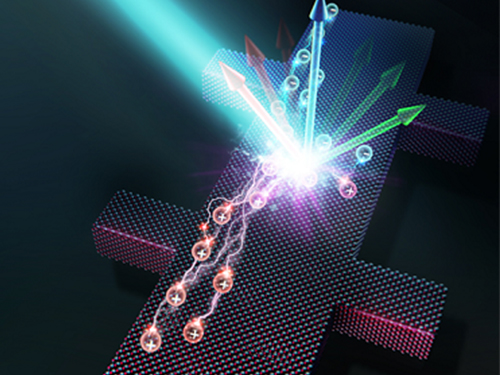 ‘Carrier-Resolved Photo-Hall’ to Push Semiconductor Advances
(Professor Shin and Dr. Gunawan (left))
An IBM-KAIST research team described a breakthrough in a 140-year-old mystery in physics. The research reported in Nature last month unlocks the physical characteristics of semiconductors in much greater detail and aids in the development of new and improved semiconductor materials.
Research team under Professor Byungha Shin at the Department of Material Sciences and Engineering and Dr. Oki Gunawan at IBM discovered a new formula and technique that enables the simultaneous extraction of both majority and minority carrier information such as their density and mobility, as well as gain additional insights about carrier lifetimes, diffusion lengths, and the recombination process. This new discovery and technology will help push semiconductor advances in both existing and emerging technologies.
Semiconductors are the basic building blocks of today’s digital electronics age, providing us with a multitude of devices that benefit our modern life. To truly appreciate the physics of semiconductors, it is very important to understand the fundamental properties of the charge carriers inside the materials, whether those particles are positive or negative, their speed under an applied electric field, and how densely they are packed into the material.
Physicist Edwin Hall found a way to determine those properties in 1879, when he discovered that a magnetic field will deflect the movement of electronic charges inside a conductor and that the amount of deflection can be measured as a voltage perpendicular to the flow of the charge. Decades after Hall’s discovery, researchers also recognized that they can measure the Hall effect with light via “photo-Hall experiments”. During such experiments, the light generates multiple carriers or electron–hole pairs in the semiconductors.
Unfortunately, the basic Hall effect only provided insights into the dominant charge carrier (or majority carrier). Researchers were unable to extract the properties of both carriers (the majority and minority carriers) simultaneously. The property information of both carriers is crucial for many applications that involve light such as solar cells and other optoelectronic devices.
In the photo-Hall experiment by the KAIST-IBM team, both carriers contribute to changes in conductivity and the Hall coefficient. The key insight comes from measuring the conductivity and Hall coefficient as a function of light intensity. Hidden in the trajectory of the conductivity, the Hall coefficient curve reveals crucial new information: the difference in the mobility of both carriers. As discussed in the paper, this relationship can be expressed elegantly as: Δµ = d (σ²H)/dσ
The research team solved for both majority and minority carrier mobility and density as a function of light intensity, naming the new technique Carrier-Resolved Photo Hall (CRPH) measurement. With known light illumination intensity, the carrier lifetime can be established in a similar way.
Beyond advances in theoretical understanding, advances in experimental techniques were also critical for enabling this breakthrough. The technique requires a clean Hall signal measurement, which can be challenging for materials where the Hall signal is weak due to low mobility or when extra unwanted signals are present, such as under strong light illumination.
The newly developed photo-Hall technique allows the extraction of an astonishing amount of information from semiconductors. In contrast to only three parameters obtained in the classic Hall measurements, this new technique yields up to seven parameters at every tested level of light intensity. These include the mobility of both the electron and hole; their carrier density under light; the recombination lifetime; and the diffusion lengths for electrons, holes, and ambipolar types. All of these can be repeated N times (i.e. the number of light intensity settings used in the experiment).
Professor Shin said, “This novel technology sheds new light on understanding the physical characteristics of semiconductor materials in great detail.” Dr. Gunawan added, “This will will help accelerate the development of next-generation semiconductor technology such as better solar cells, better optoelectronics devices, and new materials and devices for artificial intelligence technology.”
Profile:
Professor Byungha Shin
Department of Materials Science and Engineering
KAIST
byungha@kaist.ac.kr
http://energymatlab.kaist.ac.kr/
2019.11.18 View 14015
 -
 Research Day Highlights Most Outstanding Research Achievements
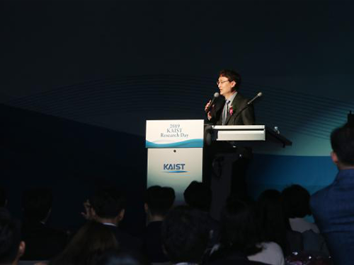
Professor Byung Jin Cho from the School of Electrical Engineering was selected as the Grand Research Prize Winner in recognition of his innovative research achievement in the fields of nano electric and flexible energy devices during the 2019 KAIST Research Day ceremony held on April 23 at the Chung Kunmo Conference Hall.
The ten most outstanding research achievements from the past year were also awarded in the three areas of Research, Innovation, Convergence Researches.
Professor Cho is an internationally recognized researcher in the field of future nano and energy device technology. Professor Cho’s team has continued to research on advanced CMOS (complementary metal-oxide semiconductors). CMOS has become his key research topic over the past three decades.
In 2014, he developed a glass fabric-based thermoelectric generator, which is extremely light and flexible and produces electricity from the heat of the human body. It is so flexible that the allowable bending radius of the generator is as low as 20 mm. There are no changes in performance even if the generator bends upward and downward for up to 120 cycles. His wearable thermoelectric generator was selected as one of the top ten most promising digital technologies by the Netexplo Forum in 2015.
He now is working on high-performance and ultra-flexible CMOS IC for biomedical applications, expanding his scope to thermal haptic technology in VR using graphene-CMOS hybrid integrated circuits; to self-powered wireless sensor nodes and self-powered ECG system using wearable thermoelectric generators .
In his special lecture at the ceremony, Professor Cho stressed the importance of collaboration in making scientific research and presented how he moved to future devices after focusing on scaling the devices.
“When I started the research on semiconductors, I focused on how to scale the device down as much as possible. For decades, we have conducted a number of procedures to produce tiny but efficient materials. Now we have shifted to develop flexible thermoelements and wearable devices,” said Professor Cho.
“We all thought the scaling down is the only way to create value-added technological breakthroughs. Now, the devices have been scaled down to 7nm and will go down to 5 nm soon. Over the past few years, I think we have gone through all the possible technological breakthroughs for reducing the size to 5nm. The semiconductor devices are made of more 1 billion transistors and go through 1,000 technological processes. So, there won’t be any possible way for a single genius to make a huge breakthrough. Without collaboration with others, it is nearly impossible to make any new technological breakthroughs.”
Professor Cho has published more than 240 papers in renowned academic journals and presented more than 300 papers at academic conferences. He has also registered approximately 50 patents in the field of semiconductor device technology.
The top ten research highlights of 2018 as follows:
- Rydberg-Atom Quantum Simulator Development by Professor Jaewook Ahn and Heung-Sun Sim from the Department of Physics
- From C-H to C-C Bonds at Room Temperature by Professor Mu-Hyun Baik from the Department of Chemistry
- The Role of Rodlike Counterions on the Interactions of DNAs by Professor Yong Woon Kim of the Graduate School of Nanoscience and Technology
- The Medal Preoptic Area Induces Hunting-Like Behaviors to Target Objects and Prey by Professor Daesoo Kim from the Department of Biological Sciences
- Identification of the Origin of Brain Tumors and New Therapeutic Strategy by Professor Jeong Ho Lee from the Graduate School of Medical Science and Engineering
- The Linear Frequency Conversion of Light at a Spatiotemporal Boundary by Professor Bumki Min from the Department of Mechanical Engineering
- An Industrial Grade Flexible Transparent Force Touch Sensor by Professor Jun-Bo Yoon from the School of Electrical Engineering
- The Detection and Clustering of Mixed-Type Defect Patterns in Wafer Bin Maps by Professor Heeyoung Kim from the Department of Industrial and Systems Engineering
- The Development of a Reconfigurable Spin-Based Logic Device by Professor Byong-Guk Park from the Department of Materials Science and Engineering
- The Development of a Miniaturized X-Ray Tube Based on Carbon Nanotube and Electronic Brachytherapy Device by Professor Sung Oh Cho from the Department of Nuclear and Quantum Engineering
Professor YongKeun Park from the Department of Physics and Professor In-Chel Park from the School of Electrical Engineering received the Research Award. For the Innovation Award, Professor Munchurl Kim from the School of Electrical Engineering was the recipient and the Convergence Research Awards was conferred to Professor Sung-Yool Choi from the School of Electrical Engineering, Professor Sung Gap Im from the Department of Chemical and Biomolecular Engineering, and Professor SangHee Park from the Department of Materials Science and Engineering during the ceremony.
For more on KAIST’s Top Research Achievements and Highlight of 2018, please refer to the attached below. click.
2019.04.25 View 15648
 -
 An Improved Carbon Nanotube Semiconductor
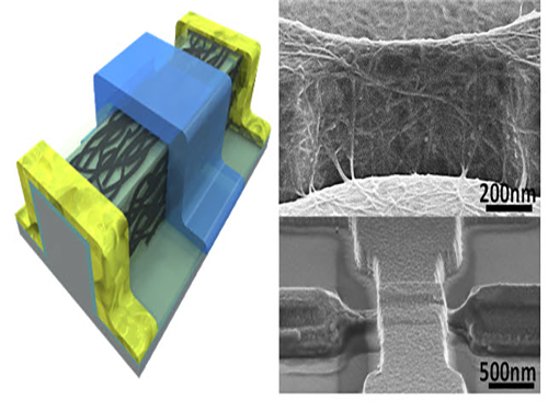
Professor Yang-Kyu Choi and his research team of the School of Electrical Engineering at KAIST collaborated with Professor Sung-Jin Choi of Kookmin University to develop a large-scale carbon nanotube semiconductor by using a 3-D fin-gate structure with carbon nanotubes on its top.
Dong Il Lee, a postdoctoral researcher at KAIST’s Electrical Engineering School, participated in this study as the first author. It was published in ACS Nano on November 10, 2016, and was entitled “Three-Dimensional Fin-Structured Semiconducting Carbon Nanotube Network Transistor.”
A semiconductor made with carbon nanotubes operates faster than a silicon semiconductor and requires less energy, yielding higher performance.
Most electronic equipment and devices, however, use silicon semiconductors because it is difficult to fabricate highly purified and densely packed semiconductors with carbon nanotubes (CNTs).
To date, the performance of CNTs was limited due to their low density. Their purity was also low, so it was impossible to make products that had a constant yield on a large-surface wafer or substrate. These characteristics made the mass production of semiconducting CNTs difficult.
To solve these difficulties, the research team used a 3-D fin-gate to vapor-deposit carbon nanotubes on its top. They developed a semiconductor that had a high current density with a width less than 50 nm.
The three-dimensional fin structure was able to vapor-deposit 600 carbon nanotubes per micrometer. This structure could have 20 times more nanotubes than the two dimensional structure, which could only vapor-deposit thirty in the same 1 micrometer width.
In addition, the research team used semi-conductive carbon nanotubes having a purity rating higher than 99.9% from a previous study to obtain a high yield semiconductor.
The semiconductor from the research group has a high current density even with a width less than 50 μm. The new semiconductor is expected to be five times faster than a silicon-based semiconductor and will require five times less electricity during operation.
Furthermore, the new semiconductor can be made by or will be compatible with the equipment for producing silicon-based semiconductors, so there will be no additional costs.
Researcher Lee said, “As a next generation semiconductor, the carbon nanotube semiconductor will have better performance, and its effectiveness will be higher.” He also added, “Hopefully, the new semiconductor will replace the silicon-based semiconductors in ten years.”
This study received support from the Center for Integrated Smart Sensors funded by the Ministry of Science, ICT & Future Planning of Korea as the Global Frontier Project, and from the CMOS (Complementary Metal-Oxide-Semiconductor) THz Technology Convergence Center of the Pioneer Research Center Program sponsored by the National Research Foundation of Korea.
Picture 1: 3D Diagram of the Carbon Nanotube Electronic Device and Its Scanning Electron Microscope (SEM) Image
Picture 2: 3D Transistor Device on an 8-inch Base and the SEM Image of Its Cross Section
2017.02.16 View 10796
 -
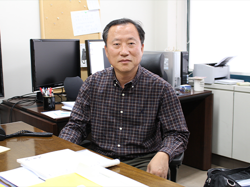 Professor Tae-Eog Lee Receives December's Scientist of the Month Award by the Korean Government
Professor Tae-Eog Lee of the Industrial and Systems Engineering at KAIST received the Scientist of the Month Award for December 2015. The award is sponsored by the Ministry of Science, ICT and Future Planning of Korea, which was hosted by the National Research Foundation of Korea.
The award recognizes Professor Lee’s efforts to advance the field of semiconductor device fabrication processing. This includes the development of the most efficient scheduling and controlling of cluster tools. He also created mathematical solutions to optimize the complicated cycle time of cluster tools in semiconductor manufacturing and the process of robot task workload.
Professor Lee contributed to the formation of various discrete event systems and automation systems based on his mathematical theories and solutions and advanced a scheduling technology for the automation of semiconductor production.
He has published 18 research papers in the past three years and has pioneered to develop Korean tool schedulers through the private sector-university cooperation.
2015.12.10 View 7572
 -
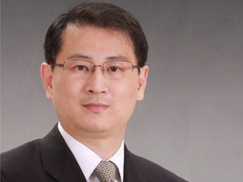 Professor Keon-Jae Lee Lectures at IEDM and ISSCC Forums
Professor Keon-Jae Lee of KAIST’s Materials Science and Engineering Department delivered a speech at the 2015 Institute of Electrical and Electronics Engineers (IEEE) International Electron Devices Meeting (IEDM) held on December 7-9, 2015 in Washington, D.C.
He will also present a speech at the 2016 International Solid-State Circuits Conference scheduled on January 31-February 4, 2016 in San Francisco, California.
Both professional gatherings are considered the world’s most renowned forums in electronic devices and semiconductor technology. It is rare for a Korean researcher to be invited to speak at these global conferences.
Professor Lee was recognized for his research on flexible NAND chips. The Korea Times, an English language daily newspaper in Korea, reported on his participation in the forums and his recent work. An excerpt of the article follows below:
“KAIST Professor to Lecture at Renowned Tech Forums”
By Lee Min-hyung, The Korea Times, November 26, 2015
Recently he has focused on delivering technologies for producing flexible materials that can be applied to everyday life. The flexible NAND flash memory chips are expected to be widely used for developing flexible handsets. His latest research also includes flexible light-emitting diodes (LED) for implantable biomedical applications.
Lee is currently running a special laboratory focused on developing new flexible nano-materials. The research group is working to develop what it calls “self-powered flexible electronic systems” using nanomaterials and electronic technology.
Lee’s achievement with flexible NAND chips was published in the October edition of Nano Letters, the renowned U.S.-based scientific journal.
He said that flexible memory chips will be used to develop wearable computers that can be installed anywhere.
2015.11.26 View 11268
 -
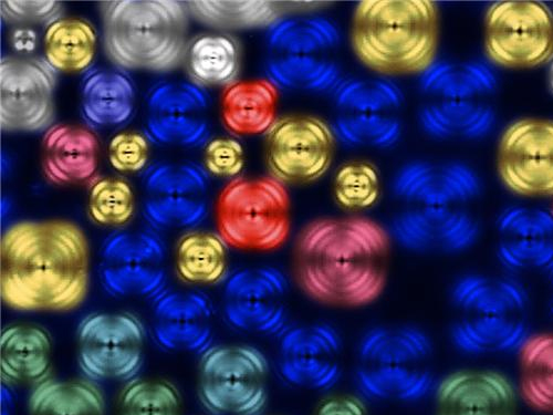 Dr. Se-Jung Kim Receives the Grand Prize at the International Photo and Image Contest on Light
Dr. Se-Jung Kim of the Physics Department at KAIST received the Grand Prize at the 2015 Photo and Image Contest of the International Year of Light and Light-based Technologies.
The United Nations has designated the year 2015 as the International Year of Light and Light-based Technologies.
The Optical Society of Korea celebrated the UN’s designation by hosting an international photo and image contest on the theme of light and optics related technology.
Dr. Kim presented a photo of images taken from a liquid crystal, which was entitled “A Micro Pinwheel.” She took pictures of liquid crystal images with a polarizing microscope and then colored the pictures. The liquid crystal has self-assembled circle domain structures, and each domain can form vortex optics. Her adviser for the project is Professor Yong-Hoon Cho of the Physics Department.
Her work was exhibited during the annual conference of the Optical Society of Korea, which was held on July 13-15, 2015 at Gyeong-Ju Hwabaek International Convention Center. It will also be exhibited at the National Science Museum in Gwacheon and the Kim Dae-Jung Convention Center in Gwangju.
Picture: A Micro Pinwheel
2015.07.31 View 10041
 -
 Professor Naehyuck Jang was Appointed Technical Program Chair of the Design Automation Conference
Professor Naehyuck Jang of the Electrical Engineering Department at KAIST was appointed as the technical program chair of the Design Automation Conference (DAC). He is the first Asian to serve the conference as the chair. At next year’s conference, he will select 150 program committee members and supervise the selection process of 1,000 papers.
Founded in 1964, DAC encompasses research related to automation of semiconductor processes, which usually involve billions of transistors. More than seven thousand people and 150 companies from all around the world participate, of which only the top 20% of the submitted papers are selected. It is the most prestigious conference in the field of semiconductor automation.
The Design Automation Conference also introduces optimization and automation of design processes of systems, hardware security, automobiles, and the Internet of things. Professor Jang specializes in low power system designs. As an ACM Distinguished Scientist, Professor Jang was elected as the chairman after contributing to this year’s program committee by reforming the process of selection of papers.
Professor Jang said, “This year’s conference represents a departure, where we move from the field of traditional semiconductors to the optimization of embedded system, the Internet of things, and security. He added that “we want to create a paper selection process that can propose the future of design automation.”
The 53rd annual DAC will take place at the Austin Convention Center in Texas in June 2016.
2015.07.02 View 6908
 -
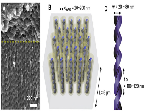 KAIST Develops Core Technology to Synthesize a Helical Nanostructure
Professor Dong-Ki Yoon’s research team of the Graduate School of Nanoscience and Technology (GSNT) at KAIST has developed helical nanostructures using self-assembly processes. The results were published in the Proceedings of the National Academy of Sciences of the United States of America(PNAS) on the October 7th.
This technology enables the synthesis of various helical structures on a relatively large confined area. Its synthesis is often considered the most arduous for three dimensional structures. Formed from liquid crystal, the structure holds a regular helical structure within the confined space of 20 to 300 nanometers. Also, the distance between each pattern increased as the diameter of the nanostructure increased.
Liquid crystals have a unique property of responding sensitively to the surrounding electromagnetic field. The technology, in combination with the electromagnetic property of liquid crystal, is expected to foster the development of highly efficient optoelectronic devices.
Using this technology, it is possible to develop three dimensional patterning technology beyond the current semiconductor manufacturing technology which uses two dimensional photolithography processes. Three-dimensional semiconductor devices are expected to store hundred times more data than current devices. They will also lower costs by simplifying manufacturing processes.
The essence of this research, “self-assembly in confined space,” refers to controlling complex nanostructures, which can be synthesized from materials such as macromolecules, liquid crystal molecules, and biomolecules in relation to surrounding environments including the temperature, concentration, and pH.
The research team produced a confined space with a length of tens of nanometers by using a porous anodized aluminum membrane induced from an electrochemical reaction. They successfully synthesized independently controlled helical nanostructures by forming the helical structures from liquid crystal molecules within that space.
Professor Yoon said, “This research examines the physicochemical principle of controlling helical nanostructures.” He highlighted the significance of the research and commented, “The technology enables the control of complex nanostructures from organic molecules by using confined space and surface reforming.”
He added that, “When grafted with nanotechnology or information technology, this technology will spur new growth to liquid crystal-related industries such as the LCD.”
The research was led by two Ph.D. candidates, Hanim Kim and Sunhee Lee, under the guidance of Professor Yoon. Dr. Tae-Joo Shin of the Pohang Accelerator Laboratory, Professor Sang-Bok Lee of the University of Maryland, and Professor Noel Clark of the University of Colorado also participated.
Picture 1. Electron Microscopy Pictures and Conceptual Diagrams of Helical Nanostructures
Picture 2. Electron Microscopy Pictures of Manufactured Helical Nanostructures
2014.10.29 View 9061