Department+of+materials+science
-
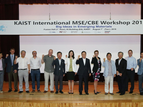 The MSE/CBE Int'l Workshop Explores Big Ideas in Emerging Materials
(KAIST President Sung-Chul Shin with scholars participated in the workshop)
The MSE/CBE International Workshop brought together editors from key academic journals in multidisciplinary materials science and scholars from leading universities at KAIST on Aug. 7.
The workshop hosted ten distinguished speakers in the fields of nanostructures for next-generation emerging applications, chemical and bio-engineering, and materials innovation for functional applications. They explored opportunities and challenges for reinventing novel materials that will solve complex problems.
(From left: Professor Buriak, Professor Swager and Professor Il-Doo Kim)
Speakers included: Chief Editor of Nature Materials Vincent Dusastre; Editor-in- Chief of ACS NANO and professor at UCLA Paul S. Weiss; Jillian M. Buriak, Editor-in-Chief of Chemistry of Materials; Associate Editor of Macromolecules and professor at MIT Timothy M. Swager; Coordinating Editor of Acta Materialia and Head of the Department of Materials Science and Engineering at MIT Christopher A. Schuh; Editor-in-Chief of Biotechnology Journal and Metabolic Engineering and Distinguished Professor at KAIST Sang-Yup Lee; Associate Editor of Energy Storage Materials and professor at KAIST Sang Ouk Kim; Professor Jeffrey C. Grossman at MIT; Professor Zhenan Bao at Stanford University; and Professor Hyuck Mo Lee, head of the Department of Materials Science and Engineering at KAIST.
Interdisciplinary materials research holds the key to building technological competitiveness in many industrial sectors extending from energy, environment, and health care to medicine and beyond. It has also been the bedrock of KAIST’s scholarship and research innovation. More than 200 faculty members in the field of materials science produce about 800 SCI papers every year. The two departments of materials science and chemical biomolecular engineering are leading KAIST’s global reputation, as they were both ranked 13th and 14th in the QS World University Ranking by Subject this year.
(Professor Il-Doo Kim fromt he Department of Materials Science Engineering)
Professor Il-Doo Kim from the Department of Materials Science Engineering has been the chair of this workshop from 2016. In hosting the second one this year, he said that he hopes this year’s workshop will inspire many materials scientists to have big ideas and work to make those big ideas get noticed in order to have a real impact.
(KAIST President Sung-Chul Shin)
President Sung-Chul Shin, who is a physicist specializing in materials physics, expressed his keen interest in the workshop, saying innovative materials made of unthinkable and noble combinations will be the key factor in determining the competitiveness of new technology and new industries. He lauded international collaborations for making new materials and the scholarly passion to evaluate the materials’ characteristics that made this significant progress possible.
Dr. Vincent Dusastre, chief editor of Nature Materials, presented recent trends in materials for energy. He described how the rational design and improvement of materials’ properties can lead to energy alternatives which will compete with existing technologies. He pointed out that given the dramatic fundamental and practical breakthroughs that are taking place in the realization of solar cells with high energy-conversion efficiency, the improvement of batteries for electric vehicles and the grid is also a major challenge. He stressed, “Key advances in sustainable approaches beyond Li-ion batteries and control of redox processes are also greatly needed.”
Meanwhile, ACS NANO Editor-in-Chief Paul S. Weiss spoke on the importance of heterogeneity in the structure and function of molecules and nanoscale assemblies. He stressed that such extensiveness of multi-interdisciplinary research will accelerate a greater impact as indicated when the fields of neuroscience and microbiome converged with nanoscience and nanotechnology.
Editor-in-Chief of Chemistry of Materials Professor Jillian M. Buriak from the University of Alberta described how predictive models and machine learning can replace time consuming empirical device production and screening. By understanding and pinpointing the frustrating bottlenecks in the design of stable and efficient organic photovoltaics, much faster throughput can be obtained to enable a more direct pathway to stability, efficiency, and finally commercialization.
2018.08.13 View 14045
 -
 A New Efficient Oxide Coating Technology to Improve Fuel Cells
A new efficient oxide coating technology that can be applied in less than five minutes could lead to dramatic improvements in the lifetime and performance of fuel cells. The fundamental principle behind this approach is maximizing the oxygen reduction reaction site of a platinum thin-film electrode, preventing the electrodes from aggregating at high temperatures.
Fuel cells have emerged as a clean electricity generation system that does not pollute the air. In particular, solid oxide fuel cells (SOFCs) are beginning to gain a great deal of attention due to their higher power generation efficiency compared to other fuel cells. It is also advantageous to use other power sources than expensive hydrogen fuel.
However, the high costs and insufficient lifetimes caused by high temperatures needed to operate the solid oxide fuel cells have remained significant challenges to commercialization.
Recently, attempts to lower the operating temperature (< 600°C) of these devices by introducing thin-film processes have drew attention of researchers, with the resulting products known as thin-film-based solid oxide fuel cells.
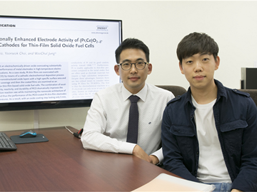
In order to create enhanced device performance at lower temperatures, the research team, led by Professor WooChul Jung in the Department of Materials Science and Engineering, applied and developed oxide coating technology to maximize the oxygen reduction reaction sites of a platinum thin-film electrode and to prevent platinum electrodes from thermal aggregating.
The team succeeded in over-coating a platinum electrode with a new coating material called praseodymium-doped ceria (Pr,Ce)O2-, which has high conductivity for both electrons and oxygen ions and excellent catalytic properties for oxygen reduction reactions. As a result, electrode resistance was reduced by more than 1000 times, creating the potential for these electrodes to be used in high-temperature electrochemical cells.
In addition, they proposed that the high performance of thin-film-based oxide fuel cells’ oxygen electrodes could be realized through the nano-structuring of (Pr,Ce)O2-δ without any platinum.
Professor Jung said, “The electrode coating technology used in this study is of great technical value because of the utilization of affordable and mass-produced electrochemical deposition.” He added, “In the future, this technology will be feasible for replacing platinum electrodes in thin-film-based oxide fuel cells, and we expect that the affordable prices of this fuel cell will eventually boost market competitiveness.”
This research was described in Advanced Energy Materials in July and was featured as the Inside Front Cover and video abstract. It was supported by the Korea Institute of Energy Technology Evaluation and Planning (KETEP) and the Korea Electric Power Corporation (KEPCO) Research Institute.
Figure 1. The change of electrode activity with and without overcoated (Pr,Ce)O2-δ nanostructures.
2018.07.18 View 8979
 -
 KAIST Team Develops Flexible Blue Vertical Micro LEDs
A KAIST research team developed a crucial source technology that will advance the commercialization of micro LEDs.
Professor Keon Jae Lee from the Department of Materials Science and Engineering and his team have developed a low cost production technology for thin-film blue flexible vertical micro LEDs (f-VLEDs).
In CES 2018, micro LED TV was spotlighted as a strong candidate for replacing the active-matrix organic light-emitting diode (AMOLED) display. Micro LED is a sub-100 um light source for red, green and blue light, which has advantages of outstanding optical output, ultra-low power consumption, fast response speed, and excellent flexibility.
However, the current display industry has utilized the individual chip transfer of millions of LED pixels, causing high production cost. Therefore, the initial market of micro LED TV will be estimated to ~ a hundred thousand dollars for global premium market.
To widely commercialize micro LEDs for mobile and TV displays, the transfer method of thin film micro LEDs requires a one-time transfer of one million LEDs. In addition, highly efficient thin-film blue micro LED is crucial for a full-color display.
The team developed thin-film red f-VLED in previous projects, and now has realized thousands of thin-film blue vertical micro LEDs (thickness < 2 μm) on plastics using a one-time transfer.
The blue GaN f-VLEDs achieved optical power density (~30 mW/mm2) three times higher than that of lateral micro LEDs, and a device lifetime of 100,000 hours by reducing heat generation. These blue f-VLEDs could be conformally attached to the curved skin and brains for wearable devices, and stably operated by wirelessly transferred electrical energy.
Professor Lee said, “For future micro LEDs, the innovative technology of thin-film transfer, efficient devices, and interconnection is necessary. We plan to demonstrate a full-color micro LED display in smart watch sizes by the end of this year. ”
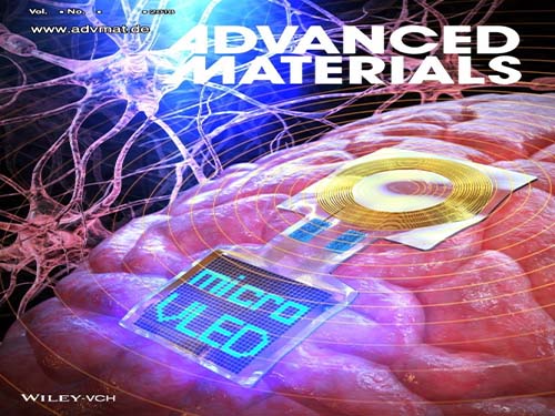
This research “ Monolithic Flexible Vertical GaN Light‐Emitting Diodes for a Transparent Wireless Brain Optical Stimulator ” led by a PhD candidate Han Eol Lee was published in the June 2018 issue of Advanced Materials.
Figure 1. Schematic image of wireless thin-film blue f-VLED arrays on the brain surface
Figure 2. Photo of high-performance and high-density blue f-VLED arrays
2018.06.18 View 9264
 -
 Platinum Catalyst Has Price Lowed and Durability Doubled
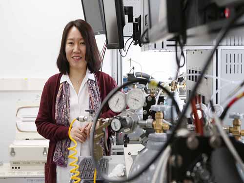
(Professor Cho in the Department of Materials Science and Engineering)
Professor EunAe Cho in the Department of Materials Science and Engineering reported a fuel cell catalyst that shows 12 times higher performance and twice the durability than previously used platinum catalyst.
Fuel cells, eco-friendly power generators, are said to be running air purifiers. A hydrogen vehicle powered by fuel cells can allegedly purify more than 98 percent of the particulate matter and ultrafine particles from the amount of air that 70 adults breathe.
Despite this peculiarity, the high price of platinum, which is used as an electrode catalyst, remains a big challenge to accelerating commercialization. In addition, recently developed ‘nano-structured platinum catalysts’ have not yet commercialized due to its meager oxygen reduction reaction and durability in fuel cell.
Addressing all those challenges, Professor Cho’s team reported a platinum catalyst costing 30 percent less but boasting 12 times higher performance.
The research team, to this end, combined the platinum with nickel, then applied various metallic elements for making the most efficient performance. Among others, they found that the addition of gallium can modulate the oxygen intermediate binding energy, leading to enhanced catalytic activity of the oxygen reduction reaction.
They made octahedron nanoparticle platinum-nickel alloy and could efficiently achieve 12-times high performance with the platinum catalyst by adding gallium to the surface of octahedron.
Existing fuel cell catalysts have issues in practical fuel cell applications. However, Professor Cho’s team experimentally proved the high performance of the catalyst even in the fuel cell, and is expected to be practically applied to the existing procedure.
First author JeongHoon Lim said their work demonstrates the gallium-added octahedral nanoparticles can be utilized as a highly active and durable oxygen reduction reaction catalyst in practical fuel cell applications. It will make it feasible for the mass production of the catalysts.
Professor Cho also said, “Our study realized the two main goals: an affordable price and increased performance of fuel cells. We hope this will make a contribution to the market competitiveness of fuel cell electric vehicles.”
This research was described in Nano Letters in April and was supported by the Korea Institute of Energy Technology Evaluation and Planning (KETEP), the National Research Foundation (NRF), and the Agency for Defense Development (ADD).
(Figure: HAADF STEM images with EDX analyses and line scanning profiles of (a) Ga-PtNi/C and (b) PtNi/C during the voltage-cycling tests. The composition changes of Ni, Pt, and Ga atoms in the nanoparticles were determined by EDX (inset in the EDX mapping results)).
2018.05.15 View 8183
 -
 Capillary Forces at Work for Lithium-Sulfur Batteries
Professor Do Kyung Kim from the KAIST Department of Materials Science and Engineering and his team succeeded in developing high-areal-capacity lithium sulfur batteries (Li-S batteries) by capturing polysulfide with carbon nanofibers. This research will provide new batteries to replace existing lithium rechargeable batteries, shifting the commercialization of related technologies ahead.
Electrical vehicles and large-scale energy storage systems necessitate the development of batteries with high energy density and cost effectiveness, and Li-S batteries are known to be one of the promising alternatives to the predominant lithium ion batteries.
With six times as much energy density, Li-S batteries theoretically thrust electric vehicle to twice the distance of lithium ion batteries. Therefore, they have been spotlighted as next-generation lithium rechargeable batteries because they can go up to 400km once charged.
However, several issues make it challenging to readily commercialize Li-S batteries. The low electrical conductivity of sulfur, volumetric expansion and contraction of the battery during charge and discharge, and permanent damage of the electrode caused by the dissolution of the lithium polysulfide into the electrolyte – known as the “shuttle effect” – are three of the biggest obstacles to commercial-grade Li-S batteries.
While there have been numerous attempts to curb, avoid, or alleviate these issues — such as the physical encapsulation of sulfur using various metal oxides or carbonaceous matrices — most of them entail utilizing zero-dimensional (0D) carbon materials. This encapsulation method has been somewhat effective in enhancing the electrical conductivity of sulfur while simultaneously tolerating some volumetric alterations and suppressing the shuttle effect. The downside of 0D carbon material-based encapsulation methods is their complicated synthetic processing and the limited mass loading of sulfur.
With this in mind, the team set out to employ one-dimensional (1D) carbon materials instead. Unlike the 0D case, 1D carbon materials render a large surface area and a long-range conduction path for electrons and lithium ions. Being 1D also solves the undesirable high-contact resistance problem frequently encountered by 0D carbon material-based encapsulation.
The key to developing the proposed material was to exploit the capillary force to decrease the energy associated with the dissolution of polysulfides. As such, carbon nanofibers (CNFs) were found to be suitable for high-areal-capacity lithium-sulfur batteries since capillary force acting between CNFs can take advantage of the high electrical conductivity with the suppressed dissolution of sulfides.
The research findings show that sulfur was successfully contained in between the CNFs by wetting due to the capillary force without the need for complicated synthetic processing, as in the 0D case. The research results indicate that the sulfur contained per unit area (mg/cm2) is five times greater for the newly implemented method, which then enabled the lithium-sulfur battery to achieve an areal capacity of 7 mAh/cm2, which amounts to as much as at most seven times that of conventional lithium ion batteries.
First author Jong Hyuk Yun stated that the unprecedented methods utilized in this study will help further and widen the progress of lithium batteries in general. Meanwhile, Professor Kim said, “This study brought us closer to commercial-grade high-capacity Li-S batteries, which are applicable for a wide variety of products, including electric vehicles, unmanned aerial vehicles (UAVs), and drones.”
This research, led by PhD candidate Yun, was published in the 18th issue of this year’s Nano Letters.
Figure 1. Electrochemical reaction leading to the containment of the sulfur within the carbon nanofiber and the corresponding specific capacity of the battery over a number of charge-discharge cycles
Figure 2. SEM images of the first discharged electrode containing lithium sulfide at the junction between the nanofibers, and the first charged electrode
Figure 3. carbon nanofiber effectively absorbing liquid based lithium polysulfide
2018.05.14 View 8548
 -
 New Material for Generating Energy-Efficient Spin Currents
(Professor Byong-Guk Park (left) and Professor Kab-Jin Kim)
Magnetic random access memory (MRAM) is emerging as next-generation memory. It allows information to be kept even without an external power supply and its unique blend of high density and high speed operation is driving global semiconductor manufacturers to develop new versions continuously.
A KAIST team, led by Professor Byong-Guk Park in the Department of Materials Science and Engineering and Professor Kab-Jin Kim in the Department of Physics, recently has developed a new material which enables the efficient generation of a spin current, the core part of operating MRAM. This new material consisting of ferromagnet-transition metal bilayers can randomly control the direction of the generated spin current unlike the existing ones.
They also described a mechanism for spin-current generation at the interface between the bottom ferromagnetic layer and the non-magnetic spacer layer, which gives torques on the top magnetic layer that are consistent with the measured magnetization dependence.
When applying this to spin-orbit torque magnetic memory, it shows the increased efficiency of spin torque and generation of the spin current without an external magnetic field. High-speed operation, the distinct feature of spin-orbit torque-based MRAM that carries its non-volatility, can significantly reduce the standby power better than SRAM.
This new material will expect to speed up the commercialization of MRAM. The research team said that this magnetic memory will further be applied to mobile, wearable, and IoT devices.
This study, conducted in collaboration with Professor Kyung-Jin Lee from Korea University and Dr. Mark Stiles from the National Institute of Standards and Technology in the US, was featured in Nature Materials in March. The research was funded by the Creative Materials Discovery Program of the Ministry of Science and ICT.
(Figure: Ferromagnet-transition metal bilayers which can randomly control the direction of the generated spin current)
2018.05.11 View 11321
 -
 KAIST Develops Sodium Ion Batteries using Copper Sulfide
A KAIST research team recently developed sodium ion batteries using copper sulfide anode. This finding will contribute to advancing the commercialization of sodium ion batteries (SIBs) and reducing the production cost of any electronic products with batteries.
Professor Jong Min Yuk and Emeritus Professor Jeong Yong Lee from Department of Materials Science and Engineering succeeded in developing a new anode material suitable for use in a SIB. Compared to the existing anode materials, the copper sulfide anode was measured to exhibit 1.5 times better cyclability with projected 40% reduction in cost.
Batteries used in various applications including mobile phones are lithium ion batteries, mostly referred as Li-ion batteries or LIBs. Though they are popularly used until now, large-scale energy storage systems require much inexpensive and abundant materials. Hence, a SIB has attracted enormous attention for their advantage over a lithium counterpart.
However, one main obstacle to commercialization of SIB is the lack of suitable anodes that exhibit high capacity and the cycling stability of the battery. Hence, the research team recognized this need for a good anode material that could offer high electrical conductivity and theoretical capacity. The material was found to be copper sulfide, preferably in nanoplates, which “prefers to make an alloy with sodium and is thus promising for high capacity and long-term cyclability.”
Further analysis presented in the study reveals that copper sulfide undergoes crystallographic tuning to make a room for sodium insertion. Results indicate that the sodium ion-insertion capacity of copper sulfide is as much as 1.5 times that of lithium ions for graphite. Furthermore, a battery with this new anode material retains 90% of its original capacity for 250 charge-discharge cycles.
With the natural abundance of sodium in seawater, this development may contribute to reduction in battery costs, which can be translated into up to 30% cut in the price of various consumer electronics.
Professor Lee expressed his hope for “the production of next-generation, high-performance sodium ion batteries”.
Professor Yuk said, “These days, people are showing a great deal of interest in products related to renewable energy due to recent micro-dust issues ongoing in Korea. This study may help Korea get a head-start on renewable energy products”.
This research, led by PhD candidate Jae Yeol Park and Dr. Sung Joo Kim, was published online in Nature Communications on March 2.
Figure 1. The sodiation process of copper sulfide
2018.04.17 View 7184
 -
 Developing Flexible Vertical Micro LED
A KAIST research team led by Professor Keon Jae Lee from the Department of Materials Science and Engineering and Professor Daesoo Kim from the Department of Biological Sciences has developed flexible vertical micro LEDs (f-VLEDs) using anisotropic conductive film (ACF)-based transfer and interconnection technology. The team also succeeded in controlling animal behavior via optogenetic stimulation of the f-VLEDs.
Flexible micro LEDs have become a strong candidate for the next-generation display due to their ultra-low power consumption, fast response speed, and excellent flexibility. However, the previous micro LED technology had critical issues such as poor device efficiency, low thermal reliability, and the lack of interconnection technology for high-resolution micro LED displays.
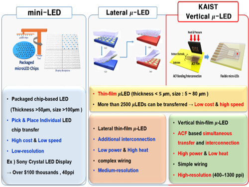
The research team has designed new transfer equipment and fabricated a f-VLED array (50ⅹ50) using simultaneous transfer and interconnection through the precise alignment of ACF bonding process. These f-VLEDs (thickness: 5 ㎛, size: below 80 ㎛) achieved optical power density (30 mW/mm2) three times higher than that of lateral micro LEDs, improving thermal reliability and lifetime by reducing heat generation within the thin film LEDs.
These f-VLEDs can be applied to optogenetics for controlling the behavior of neuron cells and brains. In contrast to the electrical stimulation that activates all of the neurons in brain, optogenetics can stimulate specific excitatory or inhibitory neurons within the localized cortical areas of the brain, which facilitates precise analysis, high-resolution mapping, and neuron modulation of animal brains. (Refer to the author’s previous ACS Nano paper of “Optogenetic Mapping of Functional Connectivity in Freely Moving Mice via Insertable Wrapping Electrode Array Beneath the Skull.” )
In this work, they inserted the innovative f-VLEDs into the narrow space between the skull and the brain surface and succeeded in controlling mouse behavior by illuminating motor neurons on two-dimensional cortical areas located deep below the brain surface.
Professor Lee said, “The flexible vertical micro LED can be used in low-power smart watches, mobile displays, and wearable lighting. In addition, these flexible optoelectronic devices are suitable for biomedical applications such as brain science, phototherapeutic treatment, and contact lens biosensors.”
He recently established a startup company ( FRONICS Inc. ) based on micro LED technology and is looking for global partnerships for commercialization. This result entitled “ Optogenetic Control of Body Movements via Flexible Vertical Light-Emitting Diodes on Brain Surface ” was published in the February 2018 issue of Nano Energy.
Figure 1. Comparison of μ-LEDs Technology
2018.01.29 View 14354
 -
 Lifespan of Fuel Cells Maximized Using Small Amount of Metals
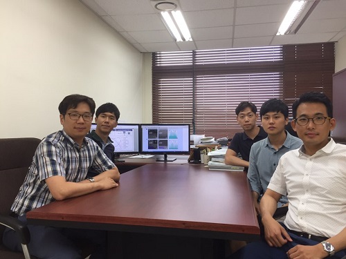
(Professor Jung (far right) and his team)
Fuel cells are key future energy technology that is emerging as eco-friendly and renewable energy sources. In particular, solid oxide fuel cells composed of ceramic materials gain increasing attention for their ability to directly convert various forms of fuel such as biomass, LNG, and LPG to electric energy.
KAIST researchers described a new technique to improve chemical stability of electrode materials which can extend the lifespan by employing a very little amount of metals.
The core factor that determines the performance of solid oxide fuel cells is the cathode at which the reduction reaction of oxygen occurs. Conventionally, oxides with perovskite structure (ABO3) are used in cathodes. However, despite the high performance of perovskite oxides at initial operation, the performance decreases with time, limiting their long-term use. In particular, the condition of high temperature oxidation state required for cathode operation leads to surface segregation phenomenon, in which second phases such as strontium oxide (SrOx) accumulate on the surface of oxides, resulting in decrease in electrode performance. The detailed mechanism of this phenomenon and a way to effectively inhibit it has not been suggested.
Using computational chemistry and experimental data, Professor WooChul Jung’s team at the Department of Materials Science and Engineering observed that local compressive states around the Sr atoms in a perovskite electrode lattice weakened the Sr-O bond strength, which in turn promote strontium segregation. The team identified local changes in strain distribution in perovskite oxide as the main cause of segregation on strontium surface. Based on these findings, the team doped different sizes of metals in oxides to control the extent of lattice strain in cathode material and effectively inhibited strontium segregation.
Professor Jung said, “This technology can be implemented by adding a small amount of metal atoms during material synthesis, without any additional process.” He continued, “I hope this technology will be useful in developing high-durable perovskite oxide electrode in the future.”
The study co-led by Professor Jung and Professor Jeong Woo Han at Department of Chemical Engineering, University of Seoul was featured as the cover of Energy and Environmental Science in the first issue of 2018.
(Figure1.Correlation between the extent of lattice strain in electrode, strontium segregation, and electrode reaction.)
(Figure 2. Cathode surface of solid oxide fuel cell stabilized using the developed technology)
2018.01.18 View 8874
 -
 A New Spin Current Generating Material Developed
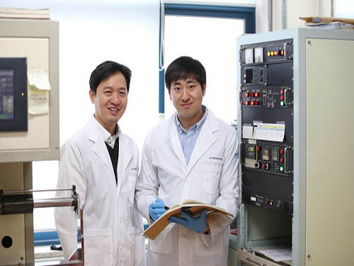
(Professor Park(left) and Ph.D. candidate Kim)
Magnetic random-access memory (MRAM) is a non-volatile device made of thin magnetic film that can maintain information without an external power supply, in contrast to conventional silicon-based semiconductor memory. It also has the potential for high-density integration and high-speed operation.
The operation of MRAM involves the control of the magnetization direction by exerting spin current-induced torque on a magnetic material. Spin current is generated using electricity in conventional MRAM, but this study developed materials technology that generates spin current using heat.
A KAIST research team led by Professor Byong-Guk Park of the Department of Materials Science and Engineering developed a material that generates spin current from heat, which can be utilized for a new operation principle for MRAM.
There have been theoretical reports on the spin Nernst effect, the phenomenon of the thermal generation of spin current, but is yet to have been experimentally proven due to technological limitations. However, the research team introduced a spin Nernst magnetoresistance measurement method using tungsten (W) and platinum (Pt) with high spin orbit coupling which allows for the experimental identification of the spin Nernst effect. They also demonstrated that the efficiency of spin current generation from heat is similar to that of spin current generated from electricity.
Professor Park said, “This research has great significance in experimentally proving spin current generation from heat, a new physical phenomenon. We aim to develop the technology as a new operational method for MRAM through further research. This can lower power consumption, and is expected to contribute to the advancement of electronics requiring low power requirement such as wearable, mobile, and IOT devices”.
This research was conducted as a joint research project with Professor Kyung-Jin Lee at Korea University and Professor Jong-Ryul Jeong at Chungnam National University. It was published in Nature Communications online on November 9 titled “Observation of transverse spin Nernst magnetoresistance induced by thermal spin current in ferromagnet/non-magnet bilayers.” Ph.D. candidate Dong-Jun Kim at KAIST is the first author. This research was funded by the Ministry of Science and ICT.
(Schematic diagram of spin Nernst magnetoresistance)
(Research result of new spin current generating materials)
2017.12.08 View 9141
 -
 Ultra-Fast and Ultra-Sensitive Hydrogen Sensor
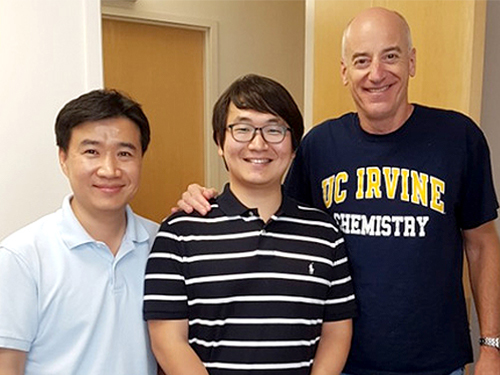
(From left: Professor Kim, Ph.D. candidate Koo, and Professor Penner)
A KAIST team made an ultra-fast hydrogen sensor that can detect hydrogen gas levels under 1% in less than seven seconds. The sensor also can detect hundreds of parts per million levels of hydrogen gas within 60 seconds at room temperature.
A research group under Professor Il-Doo Kim in the Department of Materials Science and Engineering at KAIST, in collaboration with Professor Reginald M. Penner of the University of California-Irvine, has developed an ultra-fast hydrogen gas detection system based on a palladium (Pd) nanowire array coated with a metal-organic framework (MOF).
Hydrogen has been regarded as an eco-friendly next-generation energy source. However, it is a flammable gas that can explode even with a small spark. For safety, the lower explosion limit for hydrogen gas is 4 vol% so sensors should be able to detect the colorless and odorless hydrogen molecule quickly. The importance of sensors capable of rapidly detecting colorless and odorless hydrogen gas has been emphasized in recent guidelines issued by the U.S. Department of Energy. According to the guidelines, hydrogen sensors should detect 1 vol% of hydrogen in air in less than 60 seconds for adequate response and recovery times.
To overcome the limitations of Pd-based hydrogen sensors, the research team introduced a MOF layer on top of a Pd nanowire array. Lithographically patterned Pd nanowires were simply overcoated with a Zn-based zeolite imidazole framework (ZIF-8) layer composed of Zn ions and organic ligands. ZIF-8 film is easily coated on Pd nanowires by simple dipping (for 2–6 hours) in a methanol solution including Zn (NO3)2·6H2O and 2-methylimidazole.
(This cover image depicts lithographically-patterned Pd nanowires overcoated with a Zn-based zeolite imidazole framework (ZIF-8) layer.)
As synthesized ZIF-8 is a highly porous material composed of a number of micro-pores of 0.34 nm and 1.16 nm, hydrogen gas with a kinetic diameter of 0.289 nm can easily penetrate inside the ZIF-8 membrane, while large molecules (> 0.34 nm) are effectively screened by the MOF filter. Thus, the ZIF-8 filter on the Pd nanowires allows the predominant penetration of hydrogen molecules, leading to the acceleration of Pd-based H2 sensors with a 20-fold faster recovery and response speed compared to pristine Pd nanowires at room temperature.
Professor Kim expects that the ultra-fast hydrogen sensor can be useful for the prevention of explosion accidents caused by the leakage of hydrogen gas. In addition, he expects that other harmful gases in the air can be accurately detected through effective nano-filtration by using of a variety of MOF layers.
This study was carried out by Ph.D. candidate Won-Tae Koo (first author), Professor Kim (co-corresponding author), and Professor Penner (co-corresponding author). The study has been published in the online edition of ACS Nano, as the cover-featured image for the September issue.
Figure 1. Representative image for this paper published in ACS Nano, August, 18.
Figure 2. Images of Pd nanowire array-based hydrogen sensors, scanning electron microscopy image of a Pd nanowire covered by a metal-organic framework layer, and the hydrogen sensing properties of the sensors.
Figure 3. Schematic illustration of a metal-organic framework (MOF). The MOF, consisting of metal ions and organic ligands, is a highly porous material with an ultrahigh surface area. The various structures of MOFs can be synthesized depending on the kinds of metal ions and organic ligands.
2017.09.28 View 11671
 -
 Semiconductor Patterning of Seven Nanometers Technology Using a Camera Flash
A research team led by Professor Sang Ouk Kim in the Department of Materials Science and Engineering at KAIST has developed semiconductor manufacturing technology using a camera flash.
This technology can manufacture ultra-fine patterns over a large area by irradiating a single flash with a seven-nanometer patterning technique for semiconductors. It can facilitate the manufacturing of highly efficient, integrated semiconductor devices in the future.
Technology for the Artificial Intelligence (AI), the Internet of Things (IoTs), and big data, which are the major keys for the fourth Industrial Revolution, require high-capacity, high-performance semiconductor devices. It is necessary to develop lithography technology to produce such next-generation, highly integrated semiconductor devices.
Although related industries have been using conventional photolithography for small patterns, this technique has limitations for forming a pattern of sub-10 nm patterns.
Molecular assembly patterning technology using polymers has been in the spotlight as the next generation technology to replace photolithography because it is inexpensive to produce and can easily form sub-10 nm patterns. However, since it generally takes a long time for heat treatment at high-temperature or toxic solvent vapor treatment, mass production is difficult and thus its commercialization has been limited.
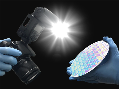
The research team introduced a camera flash that instantly emits strong light to solve the issues of polymer molecular assembly patterning. Using a flash can possibly achieve a semiconductor patterning of seven nanometers within 15 milliseconds (1 millisecond = 1/1,000 second), which can generate a temperature of several hundred degrees Celsius in several tens of milliseconds.
The team has demonstrated that applying this technology to polymer molecular assembly allows a single flash of light to form molecular assembly patterns.
The team also identified its compatibility with polymer flexible substrates, which are impossible to process at high temperatures. Through these findings, the technology can be applied to the fabrication of next-generation, flexible semiconductors.
The researchers said the camera flash photo-thermal process will be introduced into molecular assembly technology and this highly-efficiency technology can accelerate the realization of molecular assembly semiconductor technology.
Professor Kim, who led the research, said, “Despite its potential, molecular assembly semiconductor technology has remained a big challenge in improving process efficiency.” “This technology will be a breakthrough for the practical use of molecular assembly-based semiconductors.”
The paper was published in the international journal, Advanced Materials on August 21 with first authors, researcher Hyeong Min Jin and PhD candidate Dae Yong Park.
The research, sponsored by the Ministry of Science and ICT, was co-led Professor by Keon Jae Lee in the Department of Materials Science and Engineering at KAIST, and Professor Kwang Ho Kim in the School of Materials Science and Engineering at Pusan National University.
(1. Formation of semiconductor patterns using a camera flash)
(Schematic diagram of molecular assembly pattern using a camera flash)
(Self-assembled patterns)
2017.09.18 View 12314