Sung-Yool+Choi
-
 KAIST Develops Analog Memristive Synapses for Neuromorphic Chips
(Professor Sung-Yool Choi from the School of Electrical Engineering)
A KAIST research team developed a technology that makes a transition of the operation mode of flexible memristors to synaptic analog switching by reducing the size of the formed filament. Through this technology, memristors can extend their role to memristive synapses for neuromorphic chips, which will lead to developing soft neuromorphic intelligent systems.
Brain-inspired neuromorphic chips have been gaining a great deal of attention for reducing the power consumption and integrating data processing, compared to conventional semiconductor chips. Similarly, memristors are known to be the most suitable candidate for making a crossbar array which is the most efficient architecture for realizing hardware-based artificial neural network (ANN) inside a neuromorphic chip.
A hardware-based ANN consists of a neuron circuit and synapse elements, the connecting pieces. In the neuromorphic system, the synaptic weight, which represents the connection strength between neurons, should be stored and updated as the type of analog data at each synapse.
However, most memristors have digital characteristics suitable for nonvolatile memory. These characteristics put a limitation on the analog operation of the memristors, which makes it difficult to apply them to synaptic devices.
Professor Sung-Yool Choi from the School of Electrical Engineering and his team fabricated a flexible polymer memristor on a plastic substrate, and found that changing the size of the conductive metal filaments formed inside the device on the scale of metal atoms can make a transition of the memristor behavior from digital to analog.
Using this phenomenon, the team developed flexible memristor-based electronic synapses, which can continuously and linearly update synaptic weight, and operate under mechanical deformations such as bending.
The team confirmed that the ANN based on these memristor synapses can effectively classify person’s facial images even when they were damaged. This research demonstrated the possibility of a neuromorphic chip that can efficiently recognize faces, numbers, and objects.
Professor Choi said, “We found the principles underlying the transition from digital to analog operation of the memristors. I believe that this research paves the way for applying various memristors to either digital memory or electronic synapses, and will accelerate the development of a high-performing neuromorphic chip.”
In a joint research project with Professor Sung Gap Im (KAIST) and Professor V. P. Dravid (Northwestern University), this study was led by Dr. Byung Chul Jang (Samsung Electronics), Dr. Sungkyu Kim (Northwestern University) and Dr. Sang Yoon Yang (KAIST), and was published online in Nano Letters (10.1021/acs.nanolett.8b04023) on January 4, 2019.
Figure 1. a) Schematic illustration of a flexible pV3D3 memristor-based electronic synapse array. b) Cross-sectional TEM image of the flexible pV3D3 memristor
2019.02.28 View 10750
 -
 Low-power, Flexible Memristor Circuit for Mobile and Wearable Devices
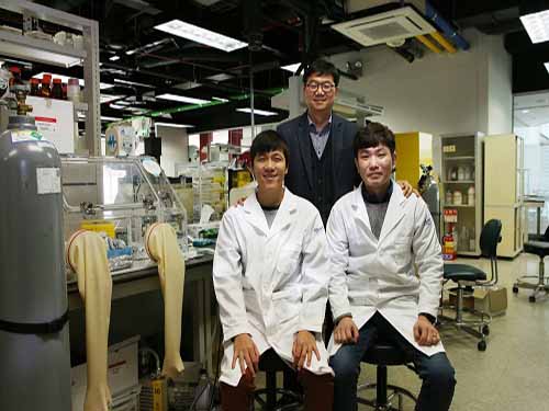
(from left: Yunyong Nam, Professor Sung-Yool Choi and Byung Chul Jang)
A KAIST research team succeeded in developing an energy efficient, nonvolatile logic-in-memory circuit by using a memristor. This novel technology can be used as an energy efficient computing architecture for battery-powered flexible electronic systems, such as mobile and wearable devices.
Professor Sung-Yool Choi from the School of Electrical Engineering and Professor Sang-Hee Ko Park from the Department of Materials Science and Engineering developed a memristive nonvolatile logic-in-memory circuit.
Transistor-based conventional electronic systems have issues with battery supply and a long standby period due to their volatile computing architecture. The standby power consumption caused by subthreshold leakage current limits their potential applications for mobile electronic devices. Also, their physical separation of memory and processor causes power consumption and time delay during data transfer.
In order to solve this problem, the team developed a logic-in-memory circuit that enables data storage as well as logic operation simultaneously. It can minimize energy consumption and time delay because it does not require data transfer between memory and processor.
The team employed nonvolatile, polymer-based memristors and flexible back-to-back Schottky diode selector devices on plastic substrates. Unlike the conventional architecture, this memristive nonvolatile logic-in-memory is a novel computing architecture that consumes a minimal amount of standby power. This one-selector-one memristor (1S-1M) solved the issue of undesirable leakage currents, known as ‘sneak currents’.
They also implemented single-instruction multiple-data (SIMD) to calculate multiple values at once.
The proposed parallel computing method using a memristive nonvolatile logic-in-memory circuit can provide a low-power circuit platform for battery-powered flexible electronic systems with a variety of potential applications.
Professor Choi said, “Flexible logic-in-memory circuits integrating memristor and selector device can provide flexibility, low power, memory with logic functions. This will be a core technology that will bring innovation to mobile and wearable electronic systems.”
This research, collaborated with Ph.D. candidates Byung Chul Jang and Yunyong Nam, was published and chosen as the cover of Advanced Functional Materials on January 10.
Figure 1. Cover of the Advanced Functional Materials
Figure 2. Schematic illustration and cross-sectional TEM image of flexible memristive nonvolatile logic-in-memory circuit
Figure 3. Test performance
Figure 4. Parallel logic operation within 1S-1M memristor array
2018.02.21 View 7181
 -
 Ultra-Low Power Flexible Memory Using 2D Materials
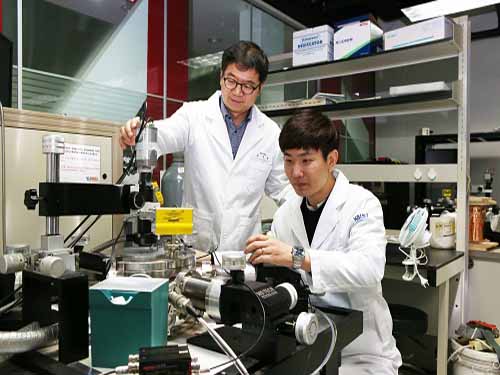
(Professor Choi and Ph.D. candidate Jang)
KAIST research team led by Professor Sung-Yool Choi at School of Electrical Engineering and Professor Sung Gap Im at the Department of Chemical and Biomolecular Engineering developed high-density, ultra-low power, non-volatile, flexible memory technology using 2D materials. The team used ultrathin molybdenum disulfide (MoS2) with atomic-scale thickness as the channel material and high-performance polymeric insulator film as the tunneling dielectric material. This research was published on the cover of Advanced Functional Materials on November 17. KAIST graduate Myung Hun Woo, a researcher at Samsung Electronics and Ph.D. candidate Byung Chul Jang are first authors.
The surge of new technologies such as Internet of Things (IoT), Artificial Intelligence (AI), and cloud server led to the paradigm shift from processor-centric computing to memory-centric computing in the industry, as well as the increase in demand of wearable devices. This led to an increased need for high-density, ultra-low power, non-volatile flexible memory. In particular, ultrathin MoS2 as semiconductor material has been recently regarded as post-silicon material. This is due to its ultrathin thickness of atomic-scale which suppresses short channel effect observed in conventional silicon material, leading to advantages in high- density and low-power consumption. Further, this thickness allows the material to be flexible, and thus the material is applicable to wearable devices.
However, due to the dangling-bond free surface of MoS2 semiconductor material, it is difficult to deposit the thin insulator film to be uniform and stable over a large area via the conventional atomic layer deposition process. Further, the currently used solution process makes it difficult to deposit uniformly low dielectric constant (k) polymeric insulator film with sub-10 nm thickness on a large area, thus indicating that the memory device utilizing the conventional solution-processed polymer insulator film cannot be operated at low-operating voltage and is not compatible with photolithography.
The research team tried to overcome the hurdles and develop high-density, ultra-low power, non-volatile flexible memory by employing a low-temperature, solvent-free, and all-dry vapor phase technique named initiated chemical vapor deposition (iCVD) process. Using iCVD process, tunneling polymeric insulator film with 10 nm thickness was deposited uniformly on MoS2 semiconductor material without being restricted by the dangling bond-free surface of MoS2. The team observed that the newly developed MoS2-based non-volatile memory can be operated at low-voltage (around 10V), in contrast to the conventional MoS2-based non-volatile memory that requires over 20V.
Professor Choi said, “As the basis for the Fourth Industrial revolution technologies including AI and IoT, semiconductor device technology needs to have characteristics of low-power and flexibility, in clear contrast to conventional memory devices.” He continued, “This new technology is significant in developing source technology in terms of materials, processes, and devices to contribute to achieve these characteristics.”
This research was supported by the Global Frontier Center for Advanced Soft Electronics and the Creative Materials Discovery Program by funded the National Research Foundation of Korea of Ministry of Science and ICT.
( Figure 1. Cover of Advanced Functional Materials)
(Figure 2. Concept map for the developed non-volatile memory material and high-resolution transmission electron microscopy image for material cross-section )
2018.01.02 View 10391
 -
 KAIST Develops a Method to Transfer Graphene by Stamping
Professor Sung-Yool Choi’s research team from KAIST's Department of Electrical Engineering has developed a technique that can produce a single-layer graphene from a metal etching. Through this, transferring a graphene layer onto a circuit board can be done as easily as stamping a seal on paper.
The research findings were published in the January 14th issue of Small as the lead article.
This technology will allow different types of wafer transfer methods such as transfer onto a surface of a device or a curved surface, and large surface transfer onto a 4 inch wafer. It will be applied in the field of wearable smart gadgets through commercialization of graphene electronic devices.
The traditional method used to transfer graphene onto a circuit board is a wet transfer. However, it has some drawbacks as the graphene layer can be damaged or contaminated during the transfer process from residue from the metal etching. This may affect the electrical properties of the transferred graphene.
After a graphene growth substrate formed on a catalytic metal substrate is pretreated in an aqueous poly vinyl alcohol (PVA) solution, a PVA film forms on the pretreated substrate. The substrate and the graphene layers bond strongly. The graphene is lifted from the growth substrate by means of an elastomeric stamp.
The delaminated graphene layer is isolated state from the elastomeric stamp and thus can be freely transferred onto a circuit board. As the catalytic metal substrate can be reused and does not contain harmful chemical substances, such transfer method is very eco-friendly.
Professor Choi said, “As the new graphene transfer method has a wide range of applications and allows a large surface transfer, it will contribute to the commercialization of graphene electronic devices.” He added that “because this technique has a high degree of freedom in transfer process, it has a variety of usages for graphene and 2 dimensional nano-devices.”
This research was sponsored by the Ministry of Science, ICT and Future Planning, the Republic of Korea.
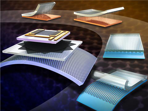
Figure 1. Cover photo of the journal Small which illustrates the research findings
Figure 2. Above view of Graphene layer transferred through the new method
Figure 3. Large surface transfer of Graphene
2015.01.23 View 12428