Yong-Hoon+Cho
-
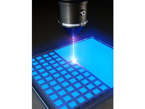 KAIST researchers develops a tech to enable production of ultrahigh-resolution LED with sub-micrometer scale pixels
Ultrahigh-resolution displays are an essential element for developing next-generation electronic products such as virtual reality (VR), augmented reality (AR), and smart watches, and can be applied not only to head-mounted displays, but also to smart glasses and smart lenses. The technology developed through this research is expected to be used to make such next-generation ultrahigh-resolution displays and other various sub-micro optoelectronic devices.
KAIST (President Kwang Hyung Lee) announced on the 22nd that Professor Yong-Hoon Cho's research team of KAIST Department of Physics developed the core technology for an ultrahigh resolution light-emitting diode (LED) display that can realize 0.5 micron-scale pixels smaller than 1/100 of the average hair thickness (about 100 microns) using focused ion beams.
Commonly, pixelation of ultrahigh-resolution LED displays usually relies on the etching method that physically cuts the area around the pixel, but as the pixel becomes smaller due to the occurrence of various defects around it, leading to side-effects of having leakage of current increased and light-emission efficiency decreased. In addition, various complex processes such as patterning for pixelation and post-processing for prevention of leakage current are required.
Professor Yong-Hoon Cho's research team developed a technology that can create pixels down to the size of a microscale without the complicated pre- and post-processing using a focused ion beam. This method has the advantage of being able to freely set the shape of the emitting pixel without causing any structural deformation on the material surface by controlling the intensity of the focused ion beam.
The focused ion beam technology has been widely used for ultrahigh-magnification imaging and nanostructure fabrication in fields such as materials engineering and biology. However, when a focused ion beam is used on a light emitting body such as an LED, light emission of a portion hit by the beam and a surrounding area rapidly decreases, which has been a barrier to fabricating a nano-scale light emitting structure. Upon facing this issue, Professor Cho's research team began the research on the idea that if they turned things around to use these problematic phenomena, they can be used in ultra-fine pixelation method on a sub-micron scale.
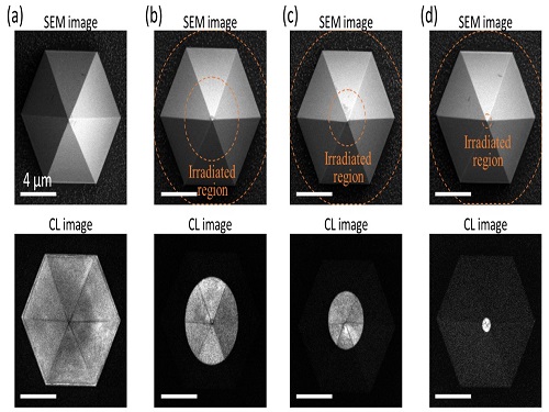
The research team used a focused ion beam whose intensity was softened to the extent that the surface was not shaved, and found that not only the light-emission rapidly decreased in the area hit by the focused ion beam, but also the local resistance greatly increased. As a result, while the surface of the LED is kept flat, the portion hit by the focused ion beam is optically and electrically isolated, enabling pixelation for independent operation.
Professor Yong-Hoon Cho, who led the research, said, “We have newly developed a technology that can create sub-micron-scale pixels without complicated processes using a focused ion beam, which will be a base technology that can be applied to next-generation ultrahigh-resolution displays and nano-photoelectronic devices.”
This research in which the Master's student Ji-Hwan Moon and the Ph.D. student Baul Kim of KAIST Department of Physics participated as co-first authors, was carried out with the support of the National Research Foundation of Korea's Support Program for Mid-Career Researchers and the Institute of Information and Communications Technology Planning and Evaluation. It was published online in 'Advanced Materials' on February 13, and was also selected as the internal cover of the next offline edition. (Title: Electrically Driven Sub-Micron Light-Emitting Diode Arrays Using Maskless and Etching-Free Pixelation)
Figure 1. Schematic diagram of the technology for ultrahigh density sub-micron-sized pixels through He focused ion beam (FIB) irradiation on an LED device
Figure 2. Ultra-high-density pixelation technology of micro light-emitting diodes (μLED) through He focused ion beam (FIB) irradiation
Figure 3. Rectangular pixels of different sizes (surface structure picture and luminescence picture) realized by a focused ion beam. Luminescence pictures of pixel arrays ranging in size from 20 µm x 20 µm to 0.5 µm x 0.5 µm, with surface flatness maintained.
2023.03.08 View 9946
 -
 Quantum Emitters: Beyond Crystal Clear to Single-Photon Pure
‘Nanoscale Focus Pinspot’ can quench only the background noise without changing the optical properties of the quantum emitter and the built-in photonic structure
Photons, fundamental particles of light, are carrying these words to your eyes via the light from your computer screen or phone. Photons play a key role in the next-generation quantum information technology, such as quantum computing and communications. A quantum emitter, capable of producing a single, pure photon, is the crux of such technology but has many issues that have yet to be solved, according to KAIST researchers.
A research team under Professor Yong-Hoon Cho has developed a technique that can isolate the desired quality emitter by reducing the noise surrounding the target with what they have dubbed a ‘nanoscale focus pinspot.’ They published their results on June 24 in ACS Nano.
“The nanoscale focus pinspot is a structurally nondestructive technique under an extremely low dose ion beam and is generally applicable for various platforms to improve their single-photon purity while retaining the integrated photonic structures,” said lead author Yong-Hoon Cho from the Department of Physics at KAIST.
To produce single photons from solid state materials, the researchers used wide-bandgap semiconductor quantum dots — fabricated nanoparticles with specialized potential properties, such as the ability to directly inject current into a small chip and to operate at room temperature for practical applications. By making a quantum dot in a photonic structure that propagates light, and then irradiating it with helium ions, researchers theorized that they could develop a quantum emitter that could reduce the unwanted noisy background and produce a single, pure photon on demand.
Professor Cho explained, “Despite its high resolution and versatility, a focused ion beam typically suppresses the optical properties around the bombarded area due to the accelerated ion beam’s high momentum. We focused on the fact that, if the focused ion beam is well controlled, only the background noise can be selectively quenched with high spatial resolution without destroying the structure.”
In other words, the researchers focused the ion beam on a mere pin prick, effectively cutting off the interactions around the quantum dot and removing the physical properties that could negatively interact with and degrade the photon purity emitted from the quantum dot.
“It is the first developed technique that can quench the background noise without changing the optical properties of the quantum emitter and the built-in photonic structure,” Professor Cho asserted.
Professor Cho compared it to stimulated emission depletion microscopy, a technique used to decrease the light around the area of focus, but leaving the focal point illuminated. The result is increased resolution of the desired visual target.
“By adjusting the focused ion beam-irradiated region, we can select the target emitter with nanoscale resolution by quenching the surrounding emitter,” Professor Cho said. “This nanoscale selective-quenching technique can be applied to various material and structural platforms and further extended for applications such as optical memory and high-resolution micro displays.” Korea’s National Research Foundation and the Samsung Science and Technology Foundation supported this work.
-PublicationMinho Choi, Seongmoon Jun, and Yong-Hoon Cho et al. ACS Nano‘Nanoscale Focus Pinspot for High-Purity Quantum Emitters via Focused-Ion-Beam-Induced Luminescence Quenching,’(https://pubs.acs.org/doi/10.1021/acsnano.1c00587)
-ProfileProfessor Yong-Hoon ChoQuantum & Nanobio Photonics Laboratoryhttp://qnp.kaist.ac.kr/
Department of PhysicsKAIST
2021.09.02 View 13388
 -
 Quantum Laser Turns Energy Loss into Gain
A new laser that generates quantum particles can recycle lost energy for highly efficient, low threshold laser applications
Scientists at KAIST have fabricated a laser system that generates highly interactive quantum particles at room temperature. Their findings, published in the journal Nature Photonics, could lead to a single microcavity laser system that requires lower threshold energy as its energy loss increases.
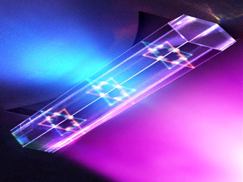
The system, developed by KAIST physicist Yong-Hoon Cho and colleagues, involves shining light through a single hexagonal-shaped microcavity treated with a loss-modulated silicon nitride substrate. The system design leads to the generation of a polariton laser at room temperature, which is exciting because this usually requires cryogenic temperatures.
The researchers found another unique and counter-intuitive feature of this design. Normally, energy is lost during laser operation. But in this system, as energy loss increased, the amount of energy needed to induce lasing decreased. Exploiting this phenomenon could lead to the development of high efficiency, low threshold lasers for future quantum optical devices.
“This system applies a concept of quantum physics known as parity-time reversal symmetry,” explains Professor Cho. “This is an important platform that allows energy loss to be used as gain. It can be used to reduce laser threshold energy for classical optical devices and sensors, as well as quantum devices and controlling the direction of light.”
The key is the design and materials. The hexagonal microcavity divides light particles into two different modes: one that passes through the upward-facing triangle of the hexagon and another that passes through its downward-facing triangle. Both modes of light particles have the same energy and path but don’t interact with each other.
However, the light particles do interact with other particles called excitons, provided by the hexagonal microcavity, which is made of semiconductors. This interaction leads to the generation of new quantum particles called polaritons that then interact with each other to generate the polariton laser. By controlling the degree of loss between the microcavity and the semiconductor substrate, an intriguing phenomenon arises, with the threshold energy becoming smaller as energy loss increases. This research was supported by the Samsung Science and Technology Foundation and Korea’s National Research Foundation.
-PublicationSong,H.G, Choi, M, Woo, K.Y. Yong-Hoon Cho Room-temperature polaritonic non-Hermitian system with single microcavityNature Photonics (https://doi.org/10.1038/s41566-021-00820-z)
-ProfileProfessor Yong-Hoon ChoQuantum & Nanobio Photonics Laboratoryhttp://qnp.kaist.ac.kr/
Department of PhysicsKAIST
2021.07.07 View 12737
 -
 Ultra-high Resolution 2-dimentional Real-time Image Capture with Super Lens
Applications to high-precision semiconductor processing or intracellular structures observation are possible.
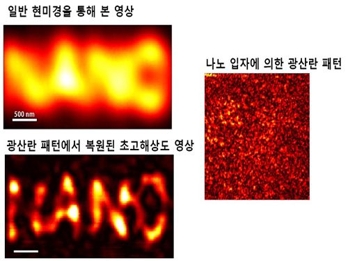
A joint research team led by Professors Yongkeun Park and Yong-Hoon Cho from the Department of Physics, KAIST, has succeeded in capturing real-time 2D images at a resolution of 100 nm (nanometers), which was impossible with optical lens due to the diffraction limit of light until now. Its future application includes high-precision semiconductor manufacturing process or observation of intracellular structures.
This research follows the past research of the super-lens developed by Professor Park last April, using paint spray to observe images that have three times higher resolution than those discovered by conventional optical lens.
Since optical lens utilize the refraction of light, the diffraction limit, which prevents achieving focus smaller than the wavelength of light, has always been a barrier for acquiring high-resolution images. In the past, it was impossible to observe objects less than the size of 200 to 300 nm in the visible light spectrum.
In order to solve the problem of near-field extinction due to scattering of light, the research team used spray paint consisting of nano-particles massed with dense scattering materials to obtain high-resolution information.
Then, by calculating and restoring the first scattering shape of light using the time reversibility of light, the researchers were able to overcome the diffraction limit. The original position of an object to be observed is obtained by deriving the complex trajectory of the light, and reversing the time to locate the particular position of the object.
Professor Park said, “This new technology can be used as the core technology in all fields which require optical measurement and control. The existing electron microscopy cannot observe cells without destroying them, but the new technology allows us to visualize at ultra-high resolution without destruction.”
The research results were published online in the 9th edition of Physical Review Letters, a prestigious international journal in the field of physics.
2014.09.23 View 11970
Ultra-high Resolution 2-dimentional Real-time Image Capture with Super Lens
Ultra-high Resolution 2-dimentional Real-time Image Capture with Super Lens
Applications to high-precision semiconductor processing or intracellular structures observation are possible.
A joint research team led by Professors Yongkeun Park and Yong-Hoon Cho from the Department of Physics, KAIST, has succeeded in capturing real-time 2D images at a resolution of 100 nm (nanometers), which was impossible with optical lens due to the diffraction limit of light until now. Its future application includes high-precision semiconductor manufacturing process or observation of intracellular structures.
This research follows the past research of the super-lens developed by Professor Park last April, using paint spray to observe images that have three times higher resolution than those discovered by conventional optical lens.
Since optical lens utilize the refraction of light, the diffraction limit, which prevents achieving focus smaller than the wavelength of light, has always been a barrier for acquiring high-resolution images. In the past, it was impossible to observe objects less than the size of 200 to 300 nm in the visible light spectrum.
In order to solve the problem of near-field extinction due to scattering of light, the research team used spray paint consisting of nano-particles massed with dense scattering materials to obtain high-resolution information.
Then, by calculating and restoring the first scattering shape of light using the time reversibility of light, the researchers were able to overcome the diffraction limit. The original position of an object to be observed is obtained by deriving the complex trajectory of the light, and reversing the time to locate the particular position of the object.
Professor Park said, “This new technology can be used as the core technology in all fields which require optical measurement and control. The existing electron microscopy cannot observe cells without destroying them, but the new technology allows us to visualize at ultra-high resolution without destruction.”
The research results were published online in the 9th edition of Physical Review Letters, a prestigious international journal in the field of physics.
2014.09.23 View 11970 -
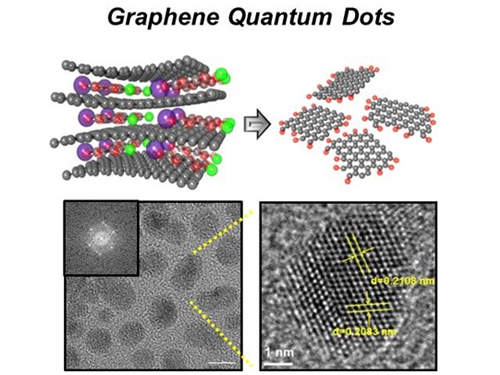 News Article on the Development of Synthesis Process for Graphene Quantum Dots
Before It's News, an international online news agency, highlighted the recent research conducted by KAIST professors (Seokwoo Jeon of the Department of Materials Science and Engineering, Yong-Hoon Cho of the Department of Physics, and Seunghyup Yoo of the Department of Electrical Engineering) on the development of synthesis process for graphene quantum dots, nanometer-sized round semiconductor nanoparticles that are very efficient at emitting photons. If commercialized, this synthetic technology will lead the way to the development of paper-thin displays in the future.
For the article, please go to the link below:
Before It’s News, September 3, 2014“Graphene quantum dots prove highly efficient in emitting light”
http://beforeitsnews.com/science-and-technology/2014/09/graphene-quantum-dots-prove-highly-efficient-in-emitting-light-2718190.html
2014.09.07 View 16486