Soft+Nanomaterials+Lab
-
 Unravelling Inherent Electrocatalysis to Improve the Performance of Hydrogen Fuel Cells
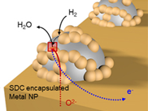
(Figure 1. Electrode structure for the precise evaluation of the metal nanoparticles’ electrochemical catalytic characteristics at a high temperature.)
A KAIST team presented an ideal electrode design to enhance the performance of high-temperature fuel cells. The new analytical platform with advanced nanoscale patterning method quantitatively revealed the electrochemical value of metal nanoparticles dispersed on the oxide electrode, thus leading to electrode design directions that can be used in a variety of eco-friendly energy technologies.
The team, working under Professor WooChul Jung and Professor Sang Ouk Kim at the Department of Materials Science and Engineering, described an accurate analysis of the reactivity of oxide electrodes boosted by metal nanoparticles, where all particles participate in the reaction. They identified how the metal catalysts activate hydrogen electro-oxidation on the ceria-based electrode surface and quantify how rapidly the reaction rate increases with the proper choice of metals.
Metal nanoparticles with diameters of 10 nanometers or less have become a key component in high-performance heterogeneous catalysts, primarily serving as a catalytic activator. Recent experimental and theoretical findings suggest that the optimization of the chemical nature at the metal and support interfaces is essential for performance improvement.
However, the high cost associated with cell fabrication and operation as well as poorer stability of metal nanoparticles at high temperatures have been a long-standing challenge. To solve this problem, the team utilized a globally recognized metal nano patterning technology that uses block copolymer self-assembled nano templates and succeeded in uniformly synthesizing metal particles 10 nanometers in size on the surface of oxide fuel cell electrodes. They also developed a technology to accurately analyze the catalyst characteristics of single particles at high temperatures and maximize the performance of a fuel cell with minimal catalyst use.
The research team confirmed that platinum, which is a commonly used metal catalyst, could boost fuel cell performance by as much as 21 times even at an amount of 300 nanograms, which only costs about 0.015 KRW.
The team quantitatively identified and compared the characteristics of widely used metal catalysts other than platinum, such as palladium, gold, and cobalt, and also elucidated the precise principle of catalyst performance through theoretical analysis.
(Figure 2. Comparison of the electrochemical catalytic characteristics for various 10nm metal nanoparticles (platinum, palladium, cobalt, gold) at a high temperature.)
Professor Jung said, "We have broken the conventional methods of increasing the amount of catalyst which have deemed inefficient and expensive. Our results suggest a clear idea for high performance fuel cells using very small amounts of nanoparticles. This technology can be applied to many different industrial fields, advancing the commercialization of eco-friendly energy technologies such as fuel cells that generate electricity and electrolytic cells that produce hydrogen from water.”
The research has been published as the cover article of Nature Nanotechnology in the March issue. This research was carried out with support from the Nano-Material Technology Development Program through the National Research Foundation of Korea.
2019.03.28 View 31148
 -
 Mussel-Inspired Defect Engineering Enhances the Mechanical Strength of Graphene Fibers
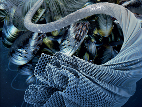
Researchers demonstrated the mussel-inspired reinforcement of graphene fibers for the improvement of different material properties. A research group under Professor Sang Ouk Kim applied polydopamine as an effective infiltrate binder to achieve high mechanical and electrical properties for graphene-based liquid crystalline fibers.
This bio-inspired defect engineering is clearly distinguishable from previous attempts with insulating binders and proposes great potential for versatile applications of flexible and wearable devices as well as low-cost structural materials. The two-step defect engineering addresses the intrinsic limitation of graphene fibers arising from the folding and wrinkling of graphene layers during the fiber-spinning process.
Bio-inspired graphene-based fiber holds great promise for a wide range of applications, including flexible electronics, multifunctional textiles, and wearable sensors. In 2009, the research group discovered graphene oxide liquid crystals in aqueous media while introducing an effective purification process to remove ionic impurities. Graphene fibers, typically wet-spun from aqueous graphene oxide liquid crystal dispersion, are expected to demonstrate superior thermal and electrical conductivities as well as outstanding mechanical performance.
Nonetheless, owing to the inherent formation of defects and voids caused by bending and wrinkling the graphene oxide layer within graphene fibers, their mechanical strength and electrical/thermal conductivities are still far below the desired ideal values. Accordingly, finding an efficient method for constructing the densely packed graphene fibers with strong interlayer interaction is a principal challenge.
Professor Kim's team focused on the adhesion properties of dopamine, a polymer developed with the inspiration of the natural mussel, to solve the problem. This functional polymer, which is studied in various fields, can increase the adhesion between the graphene layers and prevent structural defects.
Professor Kim’s research group succeeded in fabricating high-strength graphene liquid crystalline fibers with controlled structural defects. They also fabricated fibers with improved electrical conductivity through the post-carbonization process of polydopamine.
Based on the theory that dopamine with subsequent high temperature annealing has a similar structure with that of graphene, the team optimized dopamine polymerization conditions and solved the inherent defect control problems of existing graphene fibers.
They also confirmed that the physical properties of dopamine are improved in terms of electrical conductivity due to the influence of nitrogen in dopamine molecules, without damaging the conductivity, which is the fundamental limit of conventional polymers.
Professor Kim, who led the research, said, "Despite its technological potential, carbon fiber using graphene liquid crystals still has limits in terms of its structural limitations." This technology will be applied to composite fiber fabrication and various wearable textile-based application devices." This work, in which Dr. In-Ho Kim participated as first author was selected as a front cover paper of Advanced Materials on October 4.
This research was supported by the National Creative Research Initiative (CRI) Center for Multi-Dimensional Directed Nanoscale Assembly and the Nanomaterial Technology Development Program through the National Research Foundation of Korea funded by the Ministry of Science and ICT.
Figure 1. Cross-section SEM image of pure graphene fiber (left) and that of graphene fiber after two-stage defect control using polydopamine (middle and right).
2018.10.23 View 7127
 -
 Semiconductor Patterning of Seven Nanometers Technology Using a Camera Flash
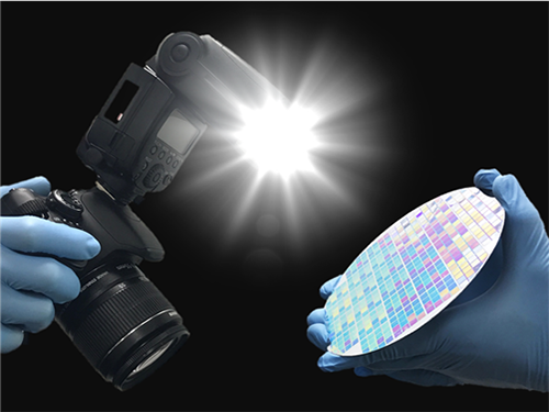
A research team led by Professor Sang Ouk Kim in the Department of Materials Science and Engineering at KAIST has developed semiconductor manufacturing technology using a camera flash.
This technology can manufacture ultra-fine patterns over a large area by irradiating a single flash with a seven-nanometer patterning technique for semiconductors. It can facilitate the manufacturing of highly efficient, integrated semiconductor devices in the future.
Technology for the Artificial Intelligence (AI), the Internet of Things (IoTs), and big data, which are the major keys for the fourth Industrial Revolution, require high-capacity, high-performance semiconductor devices. It is necessary to develop lithography technology to produce such next-generation, highly integrated semiconductor devices.
Although related industries have been using conventional photolithography for small patterns, this technique has limitations for forming a pattern of sub-10 nm patterns.
Molecular assembly patterning technology using polymers has been in the spotlight as the next generation technology to replace photolithography because it is inexpensive to produce and can easily form sub-10 nm patterns. However, since it generally takes a long time for heat treatment at high-temperature or toxic solvent vapor treatment, mass production is difficult and thus its commercialization has been limited.
The research team introduced a camera flash that instantly emits strong light to solve the issues of polymer molecular assembly patterning. Using a flash can possibly achieve a semiconductor patterning of seven nanometers within 15 milliseconds (1 millisecond = 1/1,000 second), which can generate a temperature of several hundred degrees Celsius in several tens of milliseconds.
The team has demonstrated that applying this technology to polymer molecular assembly allows a single flash of light to form molecular assembly patterns.
The team also identified its compatibility with polymer flexible substrates, which are impossible to process at high temperatures. Through these findings, the technology can be applied to the fabrication of next-generation, flexible semiconductors.
The researchers said the camera flash photo-thermal process will be introduced into molecular assembly technology and this highly-efficiency technology can accelerate the realization of molecular assembly semiconductor technology.
Professor Kim, who led the research, said, “Despite its potential, molecular assembly semiconductor technology has remained a big challenge in improving process efficiency.” “This technology will be a breakthrough for the practical use of molecular assembly-based semiconductors.”
The paper was published in the international journal, Advanced Materials on August 21 with first authors, researcher Hyeong Min Jin and PhD candidate Dae Yong Park.
The research, sponsored by the Ministry of Science and ICT, was co-led Professor by Keon Jae Lee in the Department of Materials Science and Engineering at KAIST, and Professor Kwang Ho Kim in the School of Materials Science and Engineering at Pusan National University.
(1. Formation of semiconductor patterns using a camera flash)
(Schematic diagram of molecular assembly pattern using a camera flash)
(Self-assembled patterns)
2017.09.18 View 12208
 -
 KAIST Team Develops Technology to Enable Unzipping of the Graphene Plane
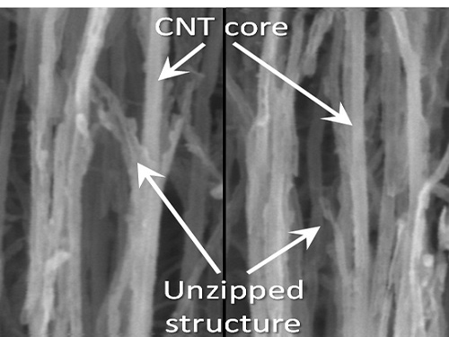
Professor Sang-Wook Kim’s research team of the Material Science and Engineering Department has developed a technique, which enables unzipping of the graphene plane without uncontrollable damage. The research findings were published online on the January 22 issue of Nature Communications.
Graphene is a form of carbon in which its atoms form a honey-comb structure through chemical bonding. If this structure can be cut to a desired form, other carbon materials with nanostructure can be created. Many researchers have tried to obtain the accurate unzipping of graphene structures, but faced challenges doing so.
To break a very strong bond between carbon atoms, an equivalently strong chemical reaction must be induced. But the chemical reaction not only cuts out the desirable borders, but also damages the surrounding ones. Conventional techniques, which cut out graphene at once, damaged the chemical properties of the graphene structure after unzipping. This is similar to wearing out paper while manipulating it.
To solve this problem, the research team adopted “heteroatom doping.” The idea is similar to a sheet of paper being split following a groove drawn on the sheet. After making some regions of the structure unstable by doping other atoms such as nitrogen on a carbon plane, the regions are electrochemically stimulated to split the parts. Nitrogen or other atoms act as the groove on the grapheme plane.
The researchers finely controlled the amount of unzipping graphene by adjusting the amount of heteroatom dopants, from which they were able to create a quality nano graphene without any damage in its 2-dimensional crystalline structure. Using this technique, the researchers were able to obtain a capacitor with state-of-the-art energy transfer speed. The nano graphene can be combined with polymer, metal, and semiconductor nano molecules to form carbon composites.
Professor Kim said, “In order to commercialize this technique, heteroatom doping should be researched further. We plan to develop fabric-like carbon materials with excellent mechanical and electrical properties using this technique.”
Picture 1: Unzipped Carbon Nano Tube
Picture 2: Development of Nano Graphene from Carbon Nano Tube Using Heteroatom Dopants
Korean descriptions translated into English:
Unzipping Process of Graphene
Carbon Nano Tube → Nano Graphen
Heteroatom
This process is similar to a paper being split in two from a tiny hole punched therein.
2016.03.22 View 9663