application
-
 KAIST Professor Jee-Hwan Ryu Receives Global IEEE Robotics Journal Best Paper Award
- Professor Jee-Hwan Ryu of Civil and Environmental Engineering receives the Best Paper Award from the Institute of Electrical and Electronics Engineers (IEEE) Robotics Journal, officially presented at ICRA, a world-renowned robotics conference.
- This is the highest level of international recognition, awarded to only the top 5 papers out of approximately 1,500 published in 2024.
- Securing a new working channel technology for soft growing robots expands the practicality and application possibilities in the field of soft robotics.
< Professor Jee-Hwan Ryu (left), Nam Gyun Kim, Ph.D. Candidate (right) from the KAIST Department of Civil and Environmental Engineering and KAIST Robotics Program >
KAIST (President Kwang-Hyung Lee) announced on the 6th that Professor Jee-Hwan Ryu from the Department of Civil and Environmental Engineering received the 2024 Best Paper Award from the Robotics and Automation Letters (RA-L), a premier journal under the IEEE, at the '2025 IEEE International Conference on Robotics and Automation (ICRA)' held in Atlanta, USA, on May 22nd.
This Best Paper Award is a prestigious honor presented to only the top 5 papers out of approximately 1,500 published in 2024, boasting high international competition and authority.
The award-winning paper by Professor Ryu proposes a novel working channel securing mechanism that significantly expands the practicality and application possibilities of 'Soft Growing Robots,' which are based on soft materials that move or perform tasks through a growing motion similar to plant roots.
< IEEE Robotics Journal Award Ceremony >
Existing soft growing robots move by inflating or contracting their bodies through increasing or decreasing internal pressure, which can lead to blockages in their internal passages. In contrast, the newly developed soft growing robot achieves a growing function while maintaining the internal passage pressure equal to the external atmospheric pressure, thereby successfully securing an internal passage while retaining the robot's flexible and soft characteristics.
This structure allows various materials or tools to be freely delivered through the internal passage (working channel) within the robot and offers the advantage of performing multi-purpose tasks by flexibly replacing equipment according to the working environment.
The research team fabricated a prototype to prove the effectiveness of this technology and verified its performance through various experiments. Specifically, in the slide plate experiment, they confirmed whether materials or equipment could pass through the robot's internal channel without obstruction, and in the pipe pulling experiment, they verified if a long pipe-shaped tool could be pulled through the internal channel.
< Figure 1. Overall hardware structure of the proposed soft growing robot (left) and a cross-sectional view composing the inflatable structure (right) >
Experimental results demonstrated that the internal channel remained stable even while the robot was growing, serving as a key basis for supporting the technology's practicality and scalability.
Professor Jee-Hwan Ryu stated, "This award is very meaningful as it signifies the global recognition of Korea's robotics technology and academic achievements. Especially, it holds great significance in achieving technical progress that can greatly expand the practicality and application fields of soft growing robots. This achievement was possible thanks to the dedication and collaboration of the research team, and I will continue to contribute to the development of robotics technology through innovative research."
< Figure 2. Material supplying mechanism of the Soft Growing Robot >
This research was co-authored by Dongoh Seo, Ph.D. Candidate in Civil and Environmental Engineering, and Nam Gyun Kim, Ph.D. Candidate in Robotics. It was published in IEEE Robotics and Automation Letters on September 1, 2024.
(Paper Title: Inflatable-Structure-Based Working-Channel Securing Mechanism for Soft Growing Robots, DOI: 10.1109/LRA.2024.3426322)
This project was supported simultaneously by the National Research Foundation of Korea's Future Promising Convergence Technology Pioneer Research Project and Mid-career Researcher Project.
2025.06.09 View 3056
KAIST Professor Jee-Hwan Ryu Receives Global IEEE Robotics Journal Best Paper Award
- Professor Jee-Hwan Ryu of Civil and Environmental Engineering receives the Best Paper Award from the Institute of Electrical and Electronics Engineers (IEEE) Robotics Journal, officially presented at ICRA, a world-renowned robotics conference.
- This is the highest level of international recognition, awarded to only the top 5 papers out of approximately 1,500 published in 2024.
- Securing a new working channel technology for soft growing robots expands the practicality and application possibilities in the field of soft robotics.
< Professor Jee-Hwan Ryu (left), Nam Gyun Kim, Ph.D. Candidate (right) from the KAIST Department of Civil and Environmental Engineering and KAIST Robotics Program >
KAIST (President Kwang-Hyung Lee) announced on the 6th that Professor Jee-Hwan Ryu from the Department of Civil and Environmental Engineering received the 2024 Best Paper Award from the Robotics and Automation Letters (RA-L), a premier journal under the IEEE, at the '2025 IEEE International Conference on Robotics and Automation (ICRA)' held in Atlanta, USA, on May 22nd.
This Best Paper Award is a prestigious honor presented to only the top 5 papers out of approximately 1,500 published in 2024, boasting high international competition and authority.
The award-winning paper by Professor Ryu proposes a novel working channel securing mechanism that significantly expands the practicality and application possibilities of 'Soft Growing Robots,' which are based on soft materials that move or perform tasks through a growing motion similar to plant roots.
< IEEE Robotics Journal Award Ceremony >
Existing soft growing robots move by inflating or contracting their bodies through increasing or decreasing internal pressure, which can lead to blockages in their internal passages. In contrast, the newly developed soft growing robot achieves a growing function while maintaining the internal passage pressure equal to the external atmospheric pressure, thereby successfully securing an internal passage while retaining the robot's flexible and soft characteristics.
This structure allows various materials or tools to be freely delivered through the internal passage (working channel) within the robot and offers the advantage of performing multi-purpose tasks by flexibly replacing equipment according to the working environment.
The research team fabricated a prototype to prove the effectiveness of this technology and verified its performance through various experiments. Specifically, in the slide plate experiment, they confirmed whether materials or equipment could pass through the robot's internal channel without obstruction, and in the pipe pulling experiment, they verified if a long pipe-shaped tool could be pulled through the internal channel.
< Figure 1. Overall hardware structure of the proposed soft growing robot (left) and a cross-sectional view composing the inflatable structure (right) >
Experimental results demonstrated that the internal channel remained stable even while the robot was growing, serving as a key basis for supporting the technology's practicality and scalability.
Professor Jee-Hwan Ryu stated, "This award is very meaningful as it signifies the global recognition of Korea's robotics technology and academic achievements. Especially, it holds great significance in achieving technical progress that can greatly expand the practicality and application fields of soft growing robots. This achievement was possible thanks to the dedication and collaboration of the research team, and I will continue to contribute to the development of robotics technology through innovative research."
< Figure 2. Material supplying mechanism of the Soft Growing Robot >
This research was co-authored by Dongoh Seo, Ph.D. Candidate in Civil and Environmental Engineering, and Nam Gyun Kim, Ph.D. Candidate in Robotics. It was published in IEEE Robotics and Automation Letters on September 1, 2024.
(Paper Title: Inflatable-Structure-Based Working-Channel Securing Mechanism for Soft Growing Robots, DOI: 10.1109/LRA.2024.3426322)
This project was supported simultaneously by the National Research Foundation of Korea's Future Promising Convergence Technology Pioneer Research Project and Mid-career Researcher Project.
2025.06.09 View 3056 -
 KAIST to Develop a Korean-style ChatGPT Platform Specifically Geared Toward Medical Diagnosis and Drug Discovery
On May 23rd, KAIST (President Kwang-Hyung Lee) announced that its Digital Bio-Health AI Research Center (Director: Professor JongChul Ye of KAIST Kim Jaechul Graduate School of AI) has been selected for the Ministry of Science and ICT's 'AI Top-Tier Young Researcher Support Program (AI Star Fellowship Project).' With a total investment of ₩11.5 billion from May 2025 to December 2030, the center will embark on the full-scale development of AI technology and a platform capable of independently inferring and determining the kinds of diseases, and discovering new drugs.
< Photo. On May 20th, a kick-off meeting for the AI Star Fellowship Project was held at KAIST Kim Jaechul Graduate School of AI’s Yangjae Research Center with the KAIST research team and participating organizations of Samsung Medical Center, NAVER Cloud, and HITS. [From left to right in the front row] Professor Jaegul Joo (KAIST), Professor Yoonjae Choi (KAIST), Professor Woo Youn Kim (KAIST/HITS), Professor JongChul Ye (KAIST), Professor Sungsoo Ahn (KAIST), Dr. Haanju Yoo (NAVER Cloud), Yoonho Lee (KAIST), HyeYoon Moon (Samsung Medical Center), Dr. Su Min Kim (Samsung Medical Center) >
This project aims to foster an innovative AI research ecosystem centered on young researchers and develop an inferential AI agent that can utilize and automatically expand specialized knowledge systems in the bio and medical fields.
Professor JongChul Ye of the Kim Jaechul Graduate School of AI will serve as the lead researcher, with young researchers from KAIST including Professors Yoonjae Choi, Kimin Lee, Sungsoo Ahn, and Chanyoung Park, along with mid-career researchers like Professors Jaegul Joo and Woo Youn Kim, jointly undertaking the project. They will collaborate with various laboratories within KAIST to conduct comprehensive research covering the entire cycle from the theoretical foundations of AI inference to its practical application.
Specifically, the main goals include: - Building high-performance inference models that integrate diverse medical knowledge systems to enhance the precision and reliability of diagnosis and treatment. - Developing a convergence inference platform that efficiently combines symbol-based inference with neural network models. - Securing AI technology for new drug development and biomarker discovery based on 'cell ontology.'
Furthermore, through close collaboration with industry and medical institutions such as Samsung Medical Center, NAVER Cloud, and HITS Co., Ltd., the project aims to achieve: - Clinical diagnostic AI utilizing medical knowledge systems. - AI-based molecular target exploration for new drug development. - Commercialization of an extendible AI inference platform.
Professor JongChul Ye, Director of KAIST's Digital Bio-Health AI Research Center, stated, "At a time when competition in AI inference model development is intensifying, it is a great honor for KAIST to lead the development of AI technology specialized in the bio and medical fields with world-class young researchers." He added, "We will do our best to ensure that the participating young researchers reach a world-leading level in terms of research achievements after the completion of this seven-year project starting in 2025."
The AI Star Fellowship is a newly established program where post-doctoral researchers and faculty members within seven years of appointment participate as project leaders (PLs) to independently lead research. Multiple laboratories within a university and demand-side companies form a consortium to operate the program.
Through this initiative, KAIST plans to nurture bio-medical convergence AI talent and simultaneously promote the commercialization of core technologies in collaboration with Samsung Medical Center, NAVER Cloud, and HITS.
2025.05.26 View 4788
KAIST to Develop a Korean-style ChatGPT Platform Specifically Geared Toward Medical Diagnosis and Drug Discovery
On May 23rd, KAIST (President Kwang-Hyung Lee) announced that its Digital Bio-Health AI Research Center (Director: Professor JongChul Ye of KAIST Kim Jaechul Graduate School of AI) has been selected for the Ministry of Science and ICT's 'AI Top-Tier Young Researcher Support Program (AI Star Fellowship Project).' With a total investment of ₩11.5 billion from May 2025 to December 2030, the center will embark on the full-scale development of AI technology and a platform capable of independently inferring and determining the kinds of diseases, and discovering new drugs.
< Photo. On May 20th, a kick-off meeting for the AI Star Fellowship Project was held at KAIST Kim Jaechul Graduate School of AI’s Yangjae Research Center with the KAIST research team and participating organizations of Samsung Medical Center, NAVER Cloud, and HITS. [From left to right in the front row] Professor Jaegul Joo (KAIST), Professor Yoonjae Choi (KAIST), Professor Woo Youn Kim (KAIST/HITS), Professor JongChul Ye (KAIST), Professor Sungsoo Ahn (KAIST), Dr. Haanju Yoo (NAVER Cloud), Yoonho Lee (KAIST), HyeYoon Moon (Samsung Medical Center), Dr. Su Min Kim (Samsung Medical Center) >
This project aims to foster an innovative AI research ecosystem centered on young researchers and develop an inferential AI agent that can utilize and automatically expand specialized knowledge systems in the bio and medical fields.
Professor JongChul Ye of the Kim Jaechul Graduate School of AI will serve as the lead researcher, with young researchers from KAIST including Professors Yoonjae Choi, Kimin Lee, Sungsoo Ahn, and Chanyoung Park, along with mid-career researchers like Professors Jaegul Joo and Woo Youn Kim, jointly undertaking the project. They will collaborate with various laboratories within KAIST to conduct comprehensive research covering the entire cycle from the theoretical foundations of AI inference to its practical application.
Specifically, the main goals include: - Building high-performance inference models that integrate diverse medical knowledge systems to enhance the precision and reliability of diagnosis and treatment. - Developing a convergence inference platform that efficiently combines symbol-based inference with neural network models. - Securing AI technology for new drug development and biomarker discovery based on 'cell ontology.'
Furthermore, through close collaboration with industry and medical institutions such as Samsung Medical Center, NAVER Cloud, and HITS Co., Ltd., the project aims to achieve: - Clinical diagnostic AI utilizing medical knowledge systems. - AI-based molecular target exploration for new drug development. - Commercialization of an extendible AI inference platform.
Professor JongChul Ye, Director of KAIST's Digital Bio-Health AI Research Center, stated, "At a time when competition in AI inference model development is intensifying, it is a great honor for KAIST to lead the development of AI technology specialized in the bio and medical fields with world-class young researchers." He added, "We will do our best to ensure that the participating young researchers reach a world-leading level in terms of research achievements after the completion of this seven-year project starting in 2025."
The AI Star Fellowship is a newly established program where post-doctoral researchers and faculty members within seven years of appointment participate as project leaders (PLs) to independently lead research. Multiple laboratories within a university and demand-side companies form a consortium to operate the program.
Through this initiative, KAIST plans to nurture bio-medical convergence AI talent and simultaneously promote the commercialization of core technologies in collaboration with Samsung Medical Center, NAVER Cloud, and HITS.
2025.05.26 View 4788 -
 KAIST Innovates Mid-Infrared Photodetectors for Exoplanet Detection, Expanding Applications to Environmental and Medical Fields
NASA’s James Webb Space Telescope (JWST) utilizes mid-infrared spectroscopy to precisely analyze molecular components such as water vapor and sulfur dioxide in exoplanet atmospheres. The key to this analysis, where each molecule exhibits a unique spectral "fingerprint," lies in highly sensitive photodetector technology capable of measuring extremely weak light intensities. Recently, KAIST researchers have developed an innovative photodetector capable of detecting a broad range of mid-infrared spectra, garnering significant attention.
< Photo 1. (from the left) Ph.D. candidate Inki Kim (co-author), Professor SangHyeon Kim (corresponding author), Dr. Joonsup Shim (first author), and Dr. Jinha Lim (co-author) of KAIST School of Electrical Engineering. >
KAIST (represented by President Kwang-Hyung Lee) announced on the 27th of March that a research team led by Professor SangHyeon Kim from the School of Electrical Engineering has developed a mid-infrared photodetector that operates stably at room temperature, marking a major turning point for the commercialization of ultra-compact optical sensors.
The newly developed photodetector utilizes conventional silicon-based CMOS processes, enabling low-cost mass production while maintaining stable operation at room temperature. Notably, the research team successfully demonstrated the real-time detection of carbon dioxide (CO₂) gas using ultra-compact and ultra-thin optical sensors equipped with this photodetector, proving its potential for environmental monitoring and hazardous gas analysis.
Existing mid-infrared photodetectors generally require cooling systems due to high thermal noise at room temperature. These cooling systems increase the size and cost of equipment, making miniaturization and integration into portable devices challenging. Furthermore, conventional mid-infrared photodetectors are incompatible with silicon-based CMOS processes, limiting large-scale production and commercialization.
To address these limitations, the research team developed a waveguide-integrated photodetector using germanium (Ge), a Group IV element like silicon. This approach enables broad-spectrum mid-infrared detection while ensuring stable operation at room temperature.
< Figure 1. Schematic diagram of a room-temperature mid-infrared waveguide-integrated photodetector based on the Ge-on-insulator optical platform proposed in this study (top). Optical microscope image of the integrated photodetector connected with the sensing unit (bottom). >
A waveguide is a structure designed to efficiently guide light along a specific path with minimal loss. To implement various optical functions on a chip (on-chip), the development of waveguide-integrated photodetectors and waveguide-based optical components is essential.
Unlike conventional photodetectors that primarily rely on bandgap absorption principles, this new technology leverages the bolometric effect*, allowing it to detect the entire mid-infrared spectral range. As a result, it can be widely applied to the real-time sensing of various molecular species.
*Bolometric effect: A principle in which light absorption leads to an increase in temperature, causing electrical signals to change accordingly.
The waveguide-integrated mid-infrared photodetector developed by the research team is considered a groundbreaking innovation that overcomes the limitations of existing mid-infrared sensor technologies, including the need for cooling, difficulties in mass production, and high costs.
< Figure 2. Room temperature photoresponse characteristics of the mid-infrared waveguide photodetector proposed in this study (left) and real-time carbon dioxide (CO2) gas sensing results using the photodetector (right). >
This breakthrough technology is expected to be applicable across diverse fields, including environmental monitoring, medical diagnostics, industrial process management, national defense and security, and smart devices. It also paves the way for next-generation mid-infrared sensor advancements.
Professor SangHyeon Kim from KAIST stated, "This research represents a novel approach that overcomes the limitations of existing mid-infrared photodetector technologies and has great potential for practical applications in various fields." He further emphasized, "Since this sensor technology is compatible with CMOS processes, it enables low-cost mass production, making it highly suitable for next-generation environmental monitoring systems and smart manufacturing sites."
< Figure 3. Performance comparison image of a room-temperature mid-infrared waveguide photodetector fabricated with the technology proposed in this study. It achieves the world’s highest performance compared to existing technologies utilizing the Bolometric effect, and is the only solution compatible with CMOS processes. The technology proposed by our research team is characterized by its ability to respond to a wide spectrum of the mid-infrared band without limitations. >
The study, with Dr. Joonsup Shim (currently a postdoctoral researcher at Harvard University) as the first author, was published on March 19, 2025 in the internationally renowned journal Light: Science & Applications (JCR 2.9%, IF=20.6).
(Paper title: “Room-temperature waveguide-integrated photodetector using bolometric effect for mid-infrared spectroscopy applications,” https://doi.org/10.1038/s41377-025-01803-3)
2025.03.27 View 3977
KAIST Innovates Mid-Infrared Photodetectors for Exoplanet Detection, Expanding Applications to Environmental and Medical Fields
NASA’s James Webb Space Telescope (JWST) utilizes mid-infrared spectroscopy to precisely analyze molecular components such as water vapor and sulfur dioxide in exoplanet atmospheres. The key to this analysis, where each molecule exhibits a unique spectral "fingerprint," lies in highly sensitive photodetector technology capable of measuring extremely weak light intensities. Recently, KAIST researchers have developed an innovative photodetector capable of detecting a broad range of mid-infrared spectra, garnering significant attention.
< Photo 1. (from the left) Ph.D. candidate Inki Kim (co-author), Professor SangHyeon Kim (corresponding author), Dr. Joonsup Shim (first author), and Dr. Jinha Lim (co-author) of KAIST School of Electrical Engineering. >
KAIST (represented by President Kwang-Hyung Lee) announced on the 27th of March that a research team led by Professor SangHyeon Kim from the School of Electrical Engineering has developed a mid-infrared photodetector that operates stably at room temperature, marking a major turning point for the commercialization of ultra-compact optical sensors.
The newly developed photodetector utilizes conventional silicon-based CMOS processes, enabling low-cost mass production while maintaining stable operation at room temperature. Notably, the research team successfully demonstrated the real-time detection of carbon dioxide (CO₂) gas using ultra-compact and ultra-thin optical sensors equipped with this photodetector, proving its potential for environmental monitoring and hazardous gas analysis.
Existing mid-infrared photodetectors generally require cooling systems due to high thermal noise at room temperature. These cooling systems increase the size and cost of equipment, making miniaturization and integration into portable devices challenging. Furthermore, conventional mid-infrared photodetectors are incompatible with silicon-based CMOS processes, limiting large-scale production and commercialization.
To address these limitations, the research team developed a waveguide-integrated photodetector using germanium (Ge), a Group IV element like silicon. This approach enables broad-spectrum mid-infrared detection while ensuring stable operation at room temperature.
< Figure 1. Schematic diagram of a room-temperature mid-infrared waveguide-integrated photodetector based on the Ge-on-insulator optical platform proposed in this study (top). Optical microscope image of the integrated photodetector connected with the sensing unit (bottom). >
A waveguide is a structure designed to efficiently guide light along a specific path with minimal loss. To implement various optical functions on a chip (on-chip), the development of waveguide-integrated photodetectors and waveguide-based optical components is essential.
Unlike conventional photodetectors that primarily rely on bandgap absorption principles, this new technology leverages the bolometric effect*, allowing it to detect the entire mid-infrared spectral range. As a result, it can be widely applied to the real-time sensing of various molecular species.
*Bolometric effect: A principle in which light absorption leads to an increase in temperature, causing electrical signals to change accordingly.
The waveguide-integrated mid-infrared photodetector developed by the research team is considered a groundbreaking innovation that overcomes the limitations of existing mid-infrared sensor technologies, including the need for cooling, difficulties in mass production, and high costs.
< Figure 2. Room temperature photoresponse characteristics of the mid-infrared waveguide photodetector proposed in this study (left) and real-time carbon dioxide (CO2) gas sensing results using the photodetector (right). >
This breakthrough technology is expected to be applicable across diverse fields, including environmental monitoring, medical diagnostics, industrial process management, national defense and security, and smart devices. It also paves the way for next-generation mid-infrared sensor advancements.
Professor SangHyeon Kim from KAIST stated, "This research represents a novel approach that overcomes the limitations of existing mid-infrared photodetector technologies and has great potential for practical applications in various fields." He further emphasized, "Since this sensor technology is compatible with CMOS processes, it enables low-cost mass production, making it highly suitable for next-generation environmental monitoring systems and smart manufacturing sites."
< Figure 3. Performance comparison image of a room-temperature mid-infrared waveguide photodetector fabricated with the technology proposed in this study. It achieves the world’s highest performance compared to existing technologies utilizing the Bolometric effect, and is the only solution compatible with CMOS processes. The technology proposed by our research team is characterized by its ability to respond to a wide spectrum of the mid-infrared band without limitations. >
The study, with Dr. Joonsup Shim (currently a postdoctoral researcher at Harvard University) as the first author, was published on March 19, 2025 in the internationally renowned journal Light: Science & Applications (JCR 2.9%, IF=20.6).
(Paper title: “Room-temperature waveguide-integrated photodetector using bolometric effect for mid-infrared spectroscopy applications,” https://doi.org/10.1038/s41377-025-01803-3)
2025.03.27 View 3977 -
 KAIST Secures Core Technology for Ultra-High-Resolution Image Sensors
A joint research team from Korea and the United States has developed next-generation, high-resolution image sensor technology with higher power efficiency and a smaller size compared to existing sensors. Notably, they have secured foundational technology for ultra-high-resolution shortwave infrared (SWIR) image sensors, an area currently dominated by Sony, paving the way for future market entry.
KAIST (represented by President Kwang Hyung Lee) announced on the 20th of November that a research team led by Professor SangHyeon Kim from the School of Electrical Engineering, in collaboration with Inha University and Yale University in the U.S., has developed an ultra-thin broadband photodiode (PD), marking a significant breakthrough in high-performance image sensor technology.
This research drastically improves the trade-off between the absorption layer thickness and quantum efficiency found in conventional photodiode technology. Specifically, it achieved high quantum efficiency of over 70% even in an absorption layer thinner than one micrometer (μm), reducing the thickness of the absorption layer by approximately 70% compared to existing technologies.
A thinner absorption layer simplifies pixel processing, allowing for higher resolution and smoother carrier diffusion, which is advantageous for light carrier acquisition while also reducing the cost. However, a fundamental issue with thinner absorption layers is the reduced absorption of long-wavelength light.
< Figure 1. Schematic diagram of the InGaAs photodiode image sensor integrated on the Guided-Mode Resonance (GMR) structure proposed in this study (left), a photograph of the fabricated wafer, and a scanning electron microscope (SEM) image of the periodic patterns (right) >
The research team introduced a guided-mode resonance (GMR) structure* that enables high-efficiency light absorption across a wide spectral range from 400 nanometers (nm) to 1,700 nanometers (nm). This wavelength range includes not only visible light but also light the SWIR region, making it valuable for various industrial applications.
*Guided-Mode Resonance (GMR) Structure: A concept used in electromagnetics, a phenomenon in which a specific (light) wave resonates (forming a strong electric/magnetic field) at a specific wavelength. Since energy is maximized under these conditions, it has been used to increase antenna or radar efficiency.
The improved performance in the SWIR region is expected to play a significant role in developing next-generation image sensors with increasingly high resolutions. The GMR structure, in particular, holds potential for further enhancing resolution and other performance metrics through hybrid integration and monolithic 3D integration with complementary metal-oxide-semiconductor (CMOS)-based readout integrated circuits (ROIC).
< Figure 2. Benchmark for state-of-the-art InGaAs-based SWIR pixels with simulated EQE lines as a function of TAL variation. Performance is maintained while reducing the absorption layer thickness from 2.1 micrometers or more to 1 micrometer or less while reducing it by 50% to 70% >
The research team has significantly enhanced international competitiveness in low-power devices and ultra-high-resolution imaging technology, opening up possibilities for applications in digital cameras, security systems, medical and industrial image sensors, as well as future ultra-high-resolution sensors for autonomous driving, aerospace, and satellite observation.
Professor Sang Hyun Kim, the lead researcher, commented, “This research demonstrates that significantly higher performance than existing technologies can be achieved even with ultra-thin absorption layers.”
< Figure 3. Top optical microscope image and cross-sectional scanning electron microscope image of the InGaAs photodiode image sensor fabricated on the GMR structure (left). Improved quantum efficiency performance of the ultra-thin image sensor (red) fabricated with the technology proposed in this study (right) >
The results of this research were published on 15th of November, in the prestigious international journal Light: Science & Applications (JCR 2.9%, IF=20.6), with Professor Dae-Myung Geum of Inha University (formerly a KAIST postdoctoral researcher) and Dr. Jinha Lim (currently a postdoctoral researcher at Yale University) as co-first authors. (Paper title: “Highly-efficient (>70%) and Wide-spectral (400 nm -1700 nm) sub-micron-thick InGaAs photodiodes for future high-resolution image sensors”)
This study was supported by the National Research Foundation of Korea.
2024.11.22 View 6926
KAIST Secures Core Technology for Ultra-High-Resolution Image Sensors
A joint research team from Korea and the United States has developed next-generation, high-resolution image sensor technology with higher power efficiency and a smaller size compared to existing sensors. Notably, they have secured foundational technology for ultra-high-resolution shortwave infrared (SWIR) image sensors, an area currently dominated by Sony, paving the way for future market entry.
KAIST (represented by President Kwang Hyung Lee) announced on the 20th of November that a research team led by Professor SangHyeon Kim from the School of Electrical Engineering, in collaboration with Inha University and Yale University in the U.S., has developed an ultra-thin broadband photodiode (PD), marking a significant breakthrough in high-performance image sensor technology.
This research drastically improves the trade-off between the absorption layer thickness and quantum efficiency found in conventional photodiode technology. Specifically, it achieved high quantum efficiency of over 70% even in an absorption layer thinner than one micrometer (μm), reducing the thickness of the absorption layer by approximately 70% compared to existing technologies.
A thinner absorption layer simplifies pixel processing, allowing for higher resolution and smoother carrier diffusion, which is advantageous for light carrier acquisition while also reducing the cost. However, a fundamental issue with thinner absorption layers is the reduced absorption of long-wavelength light.
< Figure 1. Schematic diagram of the InGaAs photodiode image sensor integrated on the Guided-Mode Resonance (GMR) structure proposed in this study (left), a photograph of the fabricated wafer, and a scanning electron microscope (SEM) image of the periodic patterns (right) >
The research team introduced a guided-mode resonance (GMR) structure* that enables high-efficiency light absorption across a wide spectral range from 400 nanometers (nm) to 1,700 nanometers (nm). This wavelength range includes not only visible light but also light the SWIR region, making it valuable for various industrial applications.
*Guided-Mode Resonance (GMR) Structure: A concept used in electromagnetics, a phenomenon in which a specific (light) wave resonates (forming a strong electric/magnetic field) at a specific wavelength. Since energy is maximized under these conditions, it has been used to increase antenna or radar efficiency.
The improved performance in the SWIR region is expected to play a significant role in developing next-generation image sensors with increasingly high resolutions. The GMR structure, in particular, holds potential for further enhancing resolution and other performance metrics through hybrid integration and monolithic 3D integration with complementary metal-oxide-semiconductor (CMOS)-based readout integrated circuits (ROIC).
< Figure 2. Benchmark for state-of-the-art InGaAs-based SWIR pixels with simulated EQE lines as a function of TAL variation. Performance is maintained while reducing the absorption layer thickness from 2.1 micrometers or more to 1 micrometer or less while reducing it by 50% to 70% >
The research team has significantly enhanced international competitiveness in low-power devices and ultra-high-resolution imaging technology, opening up possibilities for applications in digital cameras, security systems, medical and industrial image sensors, as well as future ultra-high-resolution sensors for autonomous driving, aerospace, and satellite observation.
Professor Sang Hyun Kim, the lead researcher, commented, “This research demonstrates that significantly higher performance than existing technologies can be achieved even with ultra-thin absorption layers.”
< Figure 3. Top optical microscope image and cross-sectional scanning electron microscope image of the InGaAs photodiode image sensor fabricated on the GMR structure (left). Improved quantum efficiency performance of the ultra-thin image sensor (red) fabricated with the technology proposed in this study (right) >
The results of this research were published on 15th of November, in the prestigious international journal Light: Science & Applications (JCR 2.9%, IF=20.6), with Professor Dae-Myung Geum of Inha University (formerly a KAIST postdoctoral researcher) and Dr. Jinha Lim (currently a postdoctoral researcher at Yale University) as co-first authors. (Paper title: “Highly-efficient (>70%) and Wide-spectral (400 nm -1700 nm) sub-micron-thick InGaAs photodiodes for future high-resolution image sensors”)
This study was supported by the National Research Foundation of Korea.
2024.11.22 View 6926 -
 Extremely Stable Perovskite Nanoparticles Films for Next-Generation Displays
Researchers have reported an extremely stable cross-linked perovskite nanoparticle that maintains a high photoluminescence quantum yield (PLQY) for 1.5 years in air and harsh liquid environments. This stable material’s design strategies, which addressed one of the most critical problems limiting their practical application, provide a breakthrough for the commercialization of perovskite nanoparticles in next-generation displays and bio-related applications.
According to the research team led by Professor Byeong-Soo Bae, their development can survive in severe environments such as water, various polar solvents, and high temperature with high humidity without additional encapsulation. This development is expected to enable perovskite nanoparticles to be applied to high color purity display applications as a practical color converting material. This result was published as the inside front cover article in Advanced Materials.
Perovskites, which consist of organics, metals, and halogen elements, have emerged as key elements in various optoelectronic applications. The power conversion efficiency of photovoltaic cells based on perovskites light absorbers has been rapidly increased. Perovskites are also great promise as a light emitter in display applications because of their low material cost, facile wavelength tunability, high (PLQY), very narrow emission band width, and wider color gamut than inorganic semiconducting nanocrystals and organic emitters. Thanks to these advantages, perovskites have been identified as a key color-converting material for next-generation high color-purity displays. In particular, perovskites are the only luminescence material that meets Rec. 2020 which is a new color standard in display industry.
However, perovskites are very unstable against heat, moisture, and light, which makes them almost impossible to use in practical applications. To solve these problems, many researchers have attempted to physically prevent perovskites from coming into contact with water molecules by passivating the perovskite grain and nanoparticle surfaces with organic ligands or inorganic shell materials, or by fabricating perovskite-polymer nanocomposites. These methods require complex processes and have limited stability in ambient air and water. Furthermore, stable perovskite nanoparticles in the various chemical environments and high temperatures with high humidity have not been reported yet.
The research team in collaboration with Seoul National University develops siloxane-encapsulated perovskite nanoparticle composite films. Here, perovskite nanoparticles are chemically crosslinked with thermally stable siloxane molecules, thereby significantly improving the stability of the perovskite nanoparticles without the need for any additional protecting layer.
Siloxane-encapsulated perovskite nanoparticle composite films exhibited a high PLQY (> 70%) value, which can be maintained over 600 days in water, various chemicals (alcohol, strong acidic and basic solutions), and high temperatures with high humidity (85℃/85%). The research team investigated the mechanisms impacting the chemical crosslinking and water molecule-induced stabilization of perovskite nanoparticles through various photo-physical analysis and density-functional theory calculation.
The research team confirmed that displays based on their siloxane-perovskite nanoparticle composite films exhibited higher PLQY and a wider color gamut than those of Cd-based quantum dots and demonstrated perfect color converting properties on commercial mobile phone screens. Unlike what was commonly believed in the halide perovskite field, the composite films showed excellent bio-compatibility because the siloxane matrix prevents the toxicity of Pb in perovskite nanoparticle.
By using this technology, the instability of perovskite materials, which is the biggest challenge for practical applications, is greatly improved through simple encapsulation method.
“Perovskite nanoparticle is the only photoluminescent material that can meet the next generation display color standard. Nevertheless, there has been reluctant to commercialize it due to its moisture vulnerability. The newly developed siloxane encapsulation technology will trigger more research on perovskite nanoparticles as color conversion materials and will accelerate early commercialization,” Professor Bae said.
This work was supported by the Wearable Platform Materials Technology Center (WMC) of the Engineering Research Center (ERC) Project, and the Leadership Research Program funded by the National Research Foundation of Korea.
-Publication:
Junho Jang, Young-Hoon Kim, Sunjoon Park, Dongsuk Yoo, Hyunjin Cho, Jinhyeong Jang, Han Beom Jeong, Hyunhwan Lee, Jong Min Yuk, Chan Beum Park, Duk Young Jeon, Yong-Hyun Kim, Byeong-Soo Bae, and Tae-Woo Lee. “Extremely Stable Luminescent Crosslinked Perovskite Nanoparticles under Harsh Environments over 1.5 Years” Advanced Materials, 2020, 2005255. https://doi.org/10.1002/adma.202005255.
Link to download the full-text paper:
https://onlinelibrary.wiley.com/doi/10.1002/adma.202005255
-Profile: Prof. Byeong-Soo Bae (Corresponding author)
bsbae@kaist.ac.kr
Lab. of Optical Materials & Coating
Department of Materials Science and Engineering
Korea Advanced Institute of Science and Technology (KAIST)
2020.12.29 View 16165
Extremely Stable Perovskite Nanoparticles Films for Next-Generation Displays
Researchers have reported an extremely stable cross-linked perovskite nanoparticle that maintains a high photoluminescence quantum yield (PLQY) for 1.5 years in air and harsh liquid environments. This stable material’s design strategies, which addressed one of the most critical problems limiting their practical application, provide a breakthrough for the commercialization of perovskite nanoparticles in next-generation displays and bio-related applications.
According to the research team led by Professor Byeong-Soo Bae, their development can survive in severe environments such as water, various polar solvents, and high temperature with high humidity without additional encapsulation. This development is expected to enable perovskite nanoparticles to be applied to high color purity display applications as a practical color converting material. This result was published as the inside front cover article in Advanced Materials.
Perovskites, which consist of organics, metals, and halogen elements, have emerged as key elements in various optoelectronic applications. The power conversion efficiency of photovoltaic cells based on perovskites light absorbers has been rapidly increased. Perovskites are also great promise as a light emitter in display applications because of their low material cost, facile wavelength tunability, high (PLQY), very narrow emission band width, and wider color gamut than inorganic semiconducting nanocrystals and organic emitters. Thanks to these advantages, perovskites have been identified as a key color-converting material for next-generation high color-purity displays. In particular, perovskites are the only luminescence material that meets Rec. 2020 which is a new color standard in display industry.
However, perovskites are very unstable against heat, moisture, and light, which makes them almost impossible to use in practical applications. To solve these problems, many researchers have attempted to physically prevent perovskites from coming into contact with water molecules by passivating the perovskite grain and nanoparticle surfaces with organic ligands or inorganic shell materials, or by fabricating perovskite-polymer nanocomposites. These methods require complex processes and have limited stability in ambient air and water. Furthermore, stable perovskite nanoparticles in the various chemical environments and high temperatures with high humidity have not been reported yet.
The research team in collaboration with Seoul National University develops siloxane-encapsulated perovskite nanoparticle composite films. Here, perovskite nanoparticles are chemically crosslinked with thermally stable siloxane molecules, thereby significantly improving the stability of the perovskite nanoparticles without the need for any additional protecting layer.
Siloxane-encapsulated perovskite nanoparticle composite films exhibited a high PLQY (> 70%) value, which can be maintained over 600 days in water, various chemicals (alcohol, strong acidic and basic solutions), and high temperatures with high humidity (85℃/85%). The research team investigated the mechanisms impacting the chemical crosslinking and water molecule-induced stabilization of perovskite nanoparticles through various photo-physical analysis and density-functional theory calculation.
The research team confirmed that displays based on their siloxane-perovskite nanoparticle composite films exhibited higher PLQY and a wider color gamut than those of Cd-based quantum dots and demonstrated perfect color converting properties on commercial mobile phone screens. Unlike what was commonly believed in the halide perovskite field, the composite films showed excellent bio-compatibility because the siloxane matrix prevents the toxicity of Pb in perovskite nanoparticle.
By using this technology, the instability of perovskite materials, which is the biggest challenge for practical applications, is greatly improved through simple encapsulation method.
“Perovskite nanoparticle is the only photoluminescent material that can meet the next generation display color standard. Nevertheless, there has been reluctant to commercialize it due to its moisture vulnerability. The newly developed siloxane encapsulation technology will trigger more research on perovskite nanoparticles as color conversion materials and will accelerate early commercialization,” Professor Bae said.
This work was supported by the Wearable Platform Materials Technology Center (WMC) of the Engineering Research Center (ERC) Project, and the Leadership Research Program funded by the National Research Foundation of Korea.
-Publication:
Junho Jang, Young-Hoon Kim, Sunjoon Park, Dongsuk Yoo, Hyunjin Cho, Jinhyeong Jang, Han Beom Jeong, Hyunhwan Lee, Jong Min Yuk, Chan Beum Park, Duk Young Jeon, Yong-Hyun Kim, Byeong-Soo Bae, and Tae-Woo Lee. “Extremely Stable Luminescent Crosslinked Perovskite Nanoparticles under Harsh Environments over 1.5 Years” Advanced Materials, 2020, 2005255. https://doi.org/10.1002/adma.202005255.
Link to download the full-text paper:
https://onlinelibrary.wiley.com/doi/10.1002/adma.202005255
-Profile: Prof. Byeong-Soo Bae (Corresponding author)
bsbae@kaist.ac.kr
Lab. of Optical Materials & Coating
Department of Materials Science and Engineering
Korea Advanced Institute of Science and Technology (KAIST)
2020.12.29 View 16165 -
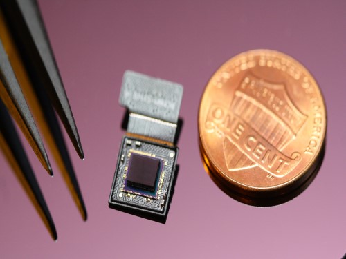 Ultrathin but Fully Packaged High-Resolution Camera
- Biologically inspired ultrathin arrayed camera captures super-resolution images. -
The unique structures of biological vision systems in nature inspired scientists to design ultracompact imaging systems. A research group led by Professor Ki-Hun Jeong have made an ultracompact camera that captures high-contrast and high-resolution images. Fully packaged with micro-optical elements such as inverted micro-lenses, multilayered pinhole arrays, and gap spacers on the image sensor, the camera boasts a total track length of 740 μm and a field of view of 73°.
Inspired by the eye structures of the paper wasp species Xenos peckii, the research team completely suppressed optical noise between micro-lenses while reducing camera thickness. The camera has successfully demonstrated high-contrast clear array images acquired from tiny micro lenses. To further enhance the image quality of the captured image, the team combined the arrayed images into one image through super-resolution imaging.
An insect’s compound eye has superior visual characteristics, such as a wide viewing angle, high motion sensitivity, and a large depth of field while maintaining a small volume of visual structure with a small focal length. Among them, the eyes of Xenos peckii and an endoparasite found on paper wasps have hundreds of photoreceptors in a single lens unlike conventional compound eyes. In particular, the eye structures of an adult Xenos peckii exhibit hundreds of photoreceptors on an individual eyelet and offer engineering inspiration for ultrathin cameras or imaging applications because they have higher visual acuity than other compound eyes.
For instance, Xenos peckii’s eye-inspired cameras provide a 50 times higher spatial resolution than those based on arthropod eyes. In addition, the effective image resolution of the Xenos peckii’s eye can be further improved using the image overlaps between neighboring eyelets. This unique structure offers higher visual resolution than other insect eyes.
The team achieved high-contrast and super-resolution imaging through a novel arrayed design of micro-optical elements comprising multilayered aperture arrays and inverted micro-lens arrays directly stacked over an image sensor. This optical component was integrated with a complementary metal oxide semiconductor image sensor.
This is first demonstration of super-resolution imaging which acquires a single integrated image with high contrast and high resolving power reconstructed from high-contrast array images. It is expected that this ultrathin arrayed camera can be applied for further developing mobile devices, advanced surveillance vehicles, and endoscopes.
Professor Jeong said, “This research has led to technological advances in imaging technology. We will continue to strive to make significant impacts on multidisciplinary research projects in the fields of microtechnology and nanotechnology, seeking inspiration from natural photonic structures.”
This work was featured in Light Science & Applications last month and was supported by the National Research Foundation (NRF) of and the Ministry of Health and Welfare (MOHW) of Korea.
Image credit: Professor Ki-Hun Jeong, KAIST
Image usage restrictions: News organizations may use or redistribute this image, with proper attribution, as part of news coverage of this paper only.
Publication:
Kisoo Kim, Kyung-Won Jang, Jae-Kwan Ryu, and Ki-Hun Jeong. (2020) “Biologically inspired ultrathin arrayed camera for high-contrast and high-resolution imaging”. Light Science & Applications. Volume 9. Article 28. Available online at https://doi.org/10.1038/s41377-020-0261-8
Profile:
Ki-Hun Jeong
Professor
kjeong@kaist.ac.kr
http://biophotonics.kaist.ac.kr/
Department of Bio and Brain Engineering
KAIST
Profile:
Kisoo Kim
Ph.D. Candidate
kisoo.kim1@kaist.ac.kr
http://biophotonics.kaist.ac.kr/
Department of Bio and Brain Engineering
KAIST
(END)
2020.03.23 View 21947
Ultrathin but Fully Packaged High-Resolution Camera
- Biologically inspired ultrathin arrayed camera captures super-resolution images. -
The unique structures of biological vision systems in nature inspired scientists to design ultracompact imaging systems. A research group led by Professor Ki-Hun Jeong have made an ultracompact camera that captures high-contrast and high-resolution images. Fully packaged with micro-optical elements such as inverted micro-lenses, multilayered pinhole arrays, and gap spacers on the image sensor, the camera boasts a total track length of 740 μm and a field of view of 73°.
Inspired by the eye structures of the paper wasp species Xenos peckii, the research team completely suppressed optical noise between micro-lenses while reducing camera thickness. The camera has successfully demonstrated high-contrast clear array images acquired from tiny micro lenses. To further enhance the image quality of the captured image, the team combined the arrayed images into one image through super-resolution imaging.
An insect’s compound eye has superior visual characteristics, such as a wide viewing angle, high motion sensitivity, and a large depth of field while maintaining a small volume of visual structure with a small focal length. Among them, the eyes of Xenos peckii and an endoparasite found on paper wasps have hundreds of photoreceptors in a single lens unlike conventional compound eyes. In particular, the eye structures of an adult Xenos peckii exhibit hundreds of photoreceptors on an individual eyelet and offer engineering inspiration for ultrathin cameras or imaging applications because they have higher visual acuity than other compound eyes.
For instance, Xenos peckii’s eye-inspired cameras provide a 50 times higher spatial resolution than those based on arthropod eyes. In addition, the effective image resolution of the Xenos peckii’s eye can be further improved using the image overlaps between neighboring eyelets. This unique structure offers higher visual resolution than other insect eyes.
The team achieved high-contrast and super-resolution imaging through a novel arrayed design of micro-optical elements comprising multilayered aperture arrays and inverted micro-lens arrays directly stacked over an image sensor. This optical component was integrated with a complementary metal oxide semiconductor image sensor.
This is first demonstration of super-resolution imaging which acquires a single integrated image with high contrast and high resolving power reconstructed from high-contrast array images. It is expected that this ultrathin arrayed camera can be applied for further developing mobile devices, advanced surveillance vehicles, and endoscopes.
Professor Jeong said, “This research has led to technological advances in imaging technology. We will continue to strive to make significant impacts on multidisciplinary research projects in the fields of microtechnology and nanotechnology, seeking inspiration from natural photonic structures.”
This work was featured in Light Science & Applications last month and was supported by the National Research Foundation (NRF) of and the Ministry of Health and Welfare (MOHW) of Korea.
Image credit: Professor Ki-Hun Jeong, KAIST
Image usage restrictions: News organizations may use or redistribute this image, with proper attribution, as part of news coverage of this paper only.
Publication:
Kisoo Kim, Kyung-Won Jang, Jae-Kwan Ryu, and Ki-Hun Jeong. (2020) “Biologically inspired ultrathin arrayed camera for high-contrast and high-resolution imaging”. Light Science & Applications. Volume 9. Article 28. Available online at https://doi.org/10.1038/s41377-020-0261-8
Profile:
Ki-Hun Jeong
Professor
kjeong@kaist.ac.kr
http://biophotonics.kaist.ac.kr/
Department of Bio and Brain Engineering
KAIST
Profile:
Kisoo Kim
Ph.D. Candidate
kisoo.kim1@kaist.ac.kr
http://biophotonics.kaist.ac.kr/
Department of Bio and Brain Engineering
KAIST
(END)
2020.03.23 View 21947 -
 Wearable Strain Sensor Using Light Transmittance Helps Measure Physical Signals Better
KAIST researchers have developed a novel wearable strain sensor based on the modulation of optical transmittance of a carbon nanotube (CNT)-embedded elastomer. The sensor is capable of sensitive, stable, and continuous measurement of physical signals. This technology, featured in the March 4th issue of ACS Applied Materials & Interfaces as a front cover article, shows great potential for the detection of subtle human motions and the real-time monitoring of body postures for healthcare applications.
A wearable strain sensor must have high sensitivity, flexibility, and stretchability, as well as low cost. Those used especially for health monitoring should also be tied to long-term solid performance, and be environmentally stable. Various stretchable strain sensors based on piezo-resistive and capacitive principles have been developed to meet all these requirements.
Conventional piezo-resistive strain sensors using functional nanomaterials, including CNTs as the most common example, have shown high sensitivity and great sensing performance. However, they suffer from poor long-term stability and linearity, as well as considerable signal hysteresis. As an alternative, piezo-capacitive strain sensors with better stability, lower hysteresis, and higher stretchability have been suggested. But due to the fact that piezo-capacitive strain sensors exhibit limited sensitivity and strong electromagnetic interference caused by the conductive objects in the surrounding environment, these conventional stretchable strain sensors are still facing limitations that are yet to be resolved.
A KAIST research team led by Professor Inkyu Park from the Department of Mechanical Engineering suggested that an optical-type stretchable strain sensor can be a good alternative to resolve the limitations of conventional piezo-resistive and piezo-capacitive strain sensors, because they have high stability and are less affected by environmental disturbances. The team then introduced an optical wearable strain sensor based on the light transmittance changes of a CNT-embedded elastomer, which further addresses the low sensitivity problem of conventional optical stretchable strain sensors.
In order to achieve a large dynamic range for the sensor, Professor Park and his researchers chose Ecoflex as an elastomeric substrate with good mechanical durability, flexibility, and attachability on human skin, and the new optical wearable strain sensor developed by the research group actually shows a wide dynamic range of 0 to 400%.
In addition, the researchers propagated the microcracks under tensile strain within the film of multi-walled CNTs embedded in the Ecoflex substrate, changing the optical transmittance of the film. By doing so, it was possible for them to develop a wearable strain sensor having a sensitivity 10 times higher than conventional optical stretchable strain sensors.
The proposed sensor has also passed the durability test with excellent results. The sensor’s response after 13,000 sets of cyclic loading was stable without any noticeable drift. This suggests that the sensor response can be used without degradation, even if the sensor is repeatedly used for a long time and in various environmental conditions.
Using the developed sensor, the research team could measure the finger bending motion and used it for robot control. They also developed a three-axes sensor array for body posture monitoring. The sensor was able to monitor human motions with small strains such as a pulse near the carotid artery and muscle movement around the mouth during pronunciation.
Professor Park said, “In this study, our group developed a new wearable strain sensor platform that overcomes many limitations of previously developed resistive, capacitive, and optical-type stretchable strain sensors. Our sensor could be widely used in a variety of fields including soft robotics, wearable electronics, electronic skin, healthcare, and even entertainment.”
This work was supported by the National Research Foundation (NRF) of Korea.
Publication:
Jimin Gu, Donguk Kwon, Junseong Ahn, and Inkyu Park. (2020) “Wearable Strain sensors Using Light Transmittance Change of Carbon Nanotube-Embedded Elastomers with Microcracks” ACS Applied Materials & Interfaces. Volume 12. Issue 9. Available online at https://doi.org/10.1021/acsami.9b18069
Profile:
Inkyu Park
Professor
inkyu@kaist.ac.kr
http://mintlab1.kaist.ac.kr
Micro/Nano Transducers Laboratory (MINT Lab)
Department of Mechanical Engineering (ME)Korea Advanced Institute of Science and Technology (KAIST)
Profile:
Jimin Gu
Ph.D. Candidate
mint9411@kaist.ac.kr
http://mintlab1.kaist.ac.kr
MINT Lab
KAIST ME
(END)
2020.03.20 View 22852
Wearable Strain Sensor Using Light Transmittance Helps Measure Physical Signals Better
KAIST researchers have developed a novel wearable strain sensor based on the modulation of optical transmittance of a carbon nanotube (CNT)-embedded elastomer. The sensor is capable of sensitive, stable, and continuous measurement of physical signals. This technology, featured in the March 4th issue of ACS Applied Materials & Interfaces as a front cover article, shows great potential for the detection of subtle human motions and the real-time monitoring of body postures for healthcare applications.
A wearable strain sensor must have high sensitivity, flexibility, and stretchability, as well as low cost. Those used especially for health monitoring should also be tied to long-term solid performance, and be environmentally stable. Various stretchable strain sensors based on piezo-resistive and capacitive principles have been developed to meet all these requirements.
Conventional piezo-resistive strain sensors using functional nanomaterials, including CNTs as the most common example, have shown high sensitivity and great sensing performance. However, they suffer from poor long-term stability and linearity, as well as considerable signal hysteresis. As an alternative, piezo-capacitive strain sensors with better stability, lower hysteresis, and higher stretchability have been suggested. But due to the fact that piezo-capacitive strain sensors exhibit limited sensitivity and strong electromagnetic interference caused by the conductive objects in the surrounding environment, these conventional stretchable strain sensors are still facing limitations that are yet to be resolved.
A KAIST research team led by Professor Inkyu Park from the Department of Mechanical Engineering suggested that an optical-type stretchable strain sensor can be a good alternative to resolve the limitations of conventional piezo-resistive and piezo-capacitive strain sensors, because they have high stability and are less affected by environmental disturbances. The team then introduced an optical wearable strain sensor based on the light transmittance changes of a CNT-embedded elastomer, which further addresses the low sensitivity problem of conventional optical stretchable strain sensors.
In order to achieve a large dynamic range for the sensor, Professor Park and his researchers chose Ecoflex as an elastomeric substrate with good mechanical durability, flexibility, and attachability on human skin, and the new optical wearable strain sensor developed by the research group actually shows a wide dynamic range of 0 to 400%.
In addition, the researchers propagated the microcracks under tensile strain within the film of multi-walled CNTs embedded in the Ecoflex substrate, changing the optical transmittance of the film. By doing so, it was possible for them to develop a wearable strain sensor having a sensitivity 10 times higher than conventional optical stretchable strain sensors.
The proposed sensor has also passed the durability test with excellent results. The sensor’s response after 13,000 sets of cyclic loading was stable without any noticeable drift. This suggests that the sensor response can be used without degradation, even if the sensor is repeatedly used for a long time and in various environmental conditions.
Using the developed sensor, the research team could measure the finger bending motion and used it for robot control. They also developed a three-axes sensor array for body posture monitoring. The sensor was able to monitor human motions with small strains such as a pulse near the carotid artery and muscle movement around the mouth during pronunciation.
Professor Park said, “In this study, our group developed a new wearable strain sensor platform that overcomes many limitations of previously developed resistive, capacitive, and optical-type stretchable strain sensors. Our sensor could be widely used in a variety of fields including soft robotics, wearable electronics, electronic skin, healthcare, and even entertainment.”
This work was supported by the National Research Foundation (NRF) of Korea.
Publication:
Jimin Gu, Donguk Kwon, Junseong Ahn, and Inkyu Park. (2020) “Wearable Strain sensors Using Light Transmittance Change of Carbon Nanotube-Embedded Elastomers with Microcracks” ACS Applied Materials & Interfaces. Volume 12. Issue 9. Available online at https://doi.org/10.1021/acsami.9b18069
Profile:
Inkyu Park
Professor
inkyu@kaist.ac.kr
http://mintlab1.kaist.ac.kr
Micro/Nano Transducers Laboratory (MINT Lab)
Department of Mechanical Engineering (ME)Korea Advanced Institute of Science and Technology (KAIST)
Profile:
Jimin Gu
Ph.D. Candidate
mint9411@kaist.ac.kr
http://mintlab1.kaist.ac.kr
MINT Lab
KAIST ME
(END)
2020.03.20 View 22852 -
 Professor Hojong Chang’s Research Team Wins ISIITA 2020 Best Paper Award
The paper written by Professor Hojong Chang’s research team from KAIST Institute for IT Convergence won the best paper award from the International Symposium on Innovation in Information Technology Application (ISIITA) 2020, held this month at Ton Duc Thang University in Vietnam.
ISIITA is a networking symposium where leading researchers from various fields including information and communications, biotechnology, and computer systems come together and share on the convergence of technology.
Professor Chang’s team won the best paper award at this year’s symposium with its paper, “A Study of Single Photon Counting System for Quantitative Analysis of Luminescence”. The awarded paper discusses the realization of a signal processing system for silicon photomultipliers.
The silicon photomultiplier is the core of a urinalysis technique that tests for sodium and potassium in the body using simple chemical reactions. If our bodily sodium and potassium levels exceed a certain amount, it can lead to high blood pressure, cardiovascular problems, and kidney damage.
Through this research, the team has developed a core technique that quantifies the sodium and potassium discharged in the urine. When the reagent is injected into the urine, a very small amount of light is emitted as a result of the chemical reaction. However, if there is a large amount of sodium and potassium, they interrupt the reaction and reduce the emission. The key to this measurement technique is digitizing the strength of this very fine emission of light. Professor Chang’s team developed a system that uses a photomultiplier to measure the chemiluminescence.
Professor Chang said, “I look forward for this signal processing system greatly helping to prevent diseases caused by the excessive consumption of sodium and potassium through quick and easy detection.”
Researcher Byunghun Han who carried out the central research for the system design added, “We are planning to focus on miniaturizing the developed technique, so that anyone can carry our device around like a cellphone.”
The research was supported by the Ministry of Science and ICT.
(END)
2020.02.27 View 12672
Professor Hojong Chang’s Research Team Wins ISIITA 2020 Best Paper Award
The paper written by Professor Hojong Chang’s research team from KAIST Institute for IT Convergence won the best paper award from the International Symposium on Innovation in Information Technology Application (ISIITA) 2020, held this month at Ton Duc Thang University in Vietnam.
ISIITA is a networking symposium where leading researchers from various fields including information and communications, biotechnology, and computer systems come together and share on the convergence of technology.
Professor Chang’s team won the best paper award at this year’s symposium with its paper, “A Study of Single Photon Counting System for Quantitative Analysis of Luminescence”. The awarded paper discusses the realization of a signal processing system for silicon photomultipliers.
The silicon photomultiplier is the core of a urinalysis technique that tests for sodium and potassium in the body using simple chemical reactions. If our bodily sodium and potassium levels exceed a certain amount, it can lead to high blood pressure, cardiovascular problems, and kidney damage.
Through this research, the team has developed a core technique that quantifies the sodium and potassium discharged in the urine. When the reagent is injected into the urine, a very small amount of light is emitted as a result of the chemical reaction. However, if there is a large amount of sodium and potassium, they interrupt the reaction and reduce the emission. The key to this measurement technique is digitizing the strength of this very fine emission of light. Professor Chang’s team developed a system that uses a photomultiplier to measure the chemiluminescence.
Professor Chang said, “I look forward for this signal processing system greatly helping to prevent diseases caused by the excessive consumption of sodium and potassium through quick and easy detection.”
Researcher Byunghun Han who carried out the central research for the system design added, “We are planning to focus on miniaturizing the developed technique, so that anyone can carry our device around like a cellphone.”
The research was supported by the Ministry of Science and ICT.
(END)
2020.02.27 View 12672 -
 Transformative Electronics Systems to Broaden Wearable Applications
Imagine a handheld electronic gadget that can soften and deform when attached to our skin. This will be the future of electronics we all dreamed of. A research team at KAIST says their new platform called 'Transformative Electronics Systems' will open a new class of electronics, allowing reconfigurable electronic interfaces to be optimized for a variety of applications.
A team working under Professor Jae-Woong Jeong from the School of Electrical Engineering at KAIST has invented a multifunctional electronic platform that can mechanically transform its shape, flexibility, and stretchability. This platform, which was reported in Science Advances, allows users to seamlessly and precisely tune its stiffness and shape.
"This new class of electronics will not only offer robust, convenient interfaces for use in both tabletop or handheld setups, but also allow seamless integration with the skin when applied onto our bodies," said Professor Jeong.
The transformative electronics consist of a special gallium metal structure, hermetically encapsulated and sealed within a soft silicone material, combined with electronics that are designed to be flexible and stretchable. The mechanical transformation of the electronic systems is specifically triggered by temperature change events controlled by the user.
"Gallium is an interesting key material. It is biocompatible, has high rigidity in solid form, and melts at a temperature comparable to the skin's temperature," said lead author Sang-Hyuk Byun, a researcher at KAIST.
Once the transformative electronic platform comes in contact with a human body, the gallium metal encapsulated inside the silicone changes to a liquid state and softens the whole electronic structure, making it stretchable, flexible, and wearable. The gallium metal then solidifies again once the structure is peeled off the skin, making the electronic circuits stiff and stable. When flexible electronic circuits were integrated onto these transformative platforms, it empowered them with the ability to become either flexible and stretchable or rigid.
"This technology could not have been achieved without interdisciplinary efforts," said co-lead author Joo Yong Sim, who is a researcher with ETRI. "We worked together with electrical, mechanical, and biomedical engineers, as well as material scientists and neuroscientists to make this breakthrough."
This universal electronics platform allowed researchers to demonstrate applications that were highly adaptable and customizable, such as a multi-purpose personal electronics with variable stiffness and stretchability, a pressure sensor with tuneable bandwidth and sensitivity, and a neural probe that softens upon implantation into brain tissue.
Applicable for both traditional and emerging electronics technologies, this breakthrough can potentially reshape the consumer electronics industry, especially in the biomedical and robotic domains. The researchers believe that with further development, this novel electronics technology can significantly impact the way we use electronics in our daily life.
< Transformative electronics in soft mode,which becomes wearable for outdoor applications.>
Video Material:
https://youtu.be/im0J18TfShk
Publication: Sang-Hyuk Byun, Joo Yong Sim, Zhanan Zhou, Juhyun Lee, Raza Qazi, Marie C. Walicki, Kyle E. Parker, Matthew P. Haney, Su Hwan Choi, Ahnsei Shon, Graydon B. Gereau, John Bilbily, Shuo Li, Yuhao Liu, Woon-Hong Yeo, Jordan G. McCall, Jianliang Xiao, and Jae-Woong Jeong. 2019. Mechanically transformative electronics, sensors, and implantable devices. Science Advances. Volume 5. No. 11. 12 pages. https://doi.org/10.1126/sciadv.aay0418
Link to download the full-text paper: https://advances.sciencemag.org/content/advances/5/11/eaay0418.full.pdf
Profile: Prof. Jae-Woong Jeong, PhD jjeong1@kaist.ac.kr
https://www.jeongresearch.org/
Professor
Bio-Integrated Electronics and Systems Laboratory
School of Electrical Engineering
Korea Advanced Institute of Science and Technology (KAIST) https://www.kaist.ac.kr
Daejeon 34141, Korea
Profile: Sang-Hyuk Byun, PhD Candidate
shbun95@kaist.ac.kr
(END)
2020.01.31 View 8512
Transformative Electronics Systems to Broaden Wearable Applications
Imagine a handheld electronic gadget that can soften and deform when attached to our skin. This will be the future of electronics we all dreamed of. A research team at KAIST says their new platform called 'Transformative Electronics Systems' will open a new class of electronics, allowing reconfigurable electronic interfaces to be optimized for a variety of applications.
A team working under Professor Jae-Woong Jeong from the School of Electrical Engineering at KAIST has invented a multifunctional electronic platform that can mechanically transform its shape, flexibility, and stretchability. This platform, which was reported in Science Advances, allows users to seamlessly and precisely tune its stiffness and shape.
"This new class of electronics will not only offer robust, convenient interfaces for use in both tabletop or handheld setups, but also allow seamless integration with the skin when applied onto our bodies," said Professor Jeong.
The transformative electronics consist of a special gallium metal structure, hermetically encapsulated and sealed within a soft silicone material, combined with electronics that are designed to be flexible and stretchable. The mechanical transformation of the electronic systems is specifically triggered by temperature change events controlled by the user.
"Gallium is an interesting key material. It is biocompatible, has high rigidity in solid form, and melts at a temperature comparable to the skin's temperature," said lead author Sang-Hyuk Byun, a researcher at KAIST.
Once the transformative electronic platform comes in contact with a human body, the gallium metal encapsulated inside the silicone changes to a liquid state and softens the whole electronic structure, making it stretchable, flexible, and wearable. The gallium metal then solidifies again once the structure is peeled off the skin, making the electronic circuits stiff and stable. When flexible electronic circuits were integrated onto these transformative platforms, it empowered them with the ability to become either flexible and stretchable or rigid.
"This technology could not have been achieved without interdisciplinary efforts," said co-lead author Joo Yong Sim, who is a researcher with ETRI. "We worked together with electrical, mechanical, and biomedical engineers, as well as material scientists and neuroscientists to make this breakthrough."
This universal electronics platform allowed researchers to demonstrate applications that were highly adaptable and customizable, such as a multi-purpose personal electronics with variable stiffness and stretchability, a pressure sensor with tuneable bandwidth and sensitivity, and a neural probe that softens upon implantation into brain tissue.
Applicable for both traditional and emerging electronics technologies, this breakthrough can potentially reshape the consumer electronics industry, especially in the biomedical and robotic domains. The researchers believe that with further development, this novel electronics technology can significantly impact the way we use electronics in our daily life.
< Transformative electronics in soft mode,which becomes wearable for outdoor applications.>
Video Material:
https://youtu.be/im0J18TfShk
Publication: Sang-Hyuk Byun, Joo Yong Sim, Zhanan Zhou, Juhyun Lee, Raza Qazi, Marie C. Walicki, Kyle E. Parker, Matthew P. Haney, Su Hwan Choi, Ahnsei Shon, Graydon B. Gereau, John Bilbily, Shuo Li, Yuhao Liu, Woon-Hong Yeo, Jordan G. McCall, Jianliang Xiao, and Jae-Woong Jeong. 2019. Mechanically transformative electronics, sensors, and implantable devices. Science Advances. Volume 5. No. 11. 12 pages. https://doi.org/10.1126/sciadv.aay0418
Link to download the full-text paper: https://advances.sciencemag.org/content/advances/5/11/eaay0418.full.pdf
Profile: Prof. Jae-Woong Jeong, PhD jjeong1@kaist.ac.kr
https://www.jeongresearch.org/
Professor
Bio-Integrated Electronics and Systems Laboratory
School of Electrical Engineering
Korea Advanced Institute of Science and Technology (KAIST) https://www.kaist.ac.kr
Daejeon 34141, Korea
Profile: Sang-Hyuk Byun, PhD Candidate
shbun95@kaist.ac.kr
(END)
2020.01.31 View 8512 -
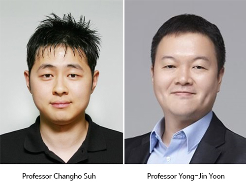 KAIST and Google Jointly Develop AI Curricula
KAIST selected the two professors who will develop AI curriculum under the auspices of the KAIST-Google Partnership for AI Education and Research. The Graduate School of AI announced the two authors among the 20 applicants who will develop the curriculum next year. They will be provided 7,500 USD per subject.
Professor Changho Suh from the School of Electrical Engineering and Professor Yong-Jin Yoon from the Department of Mechanical Engineering will use Google technology such as TensorFlow, Google Cloud, and Android to create the curriculum.
Professor Suh’s “TensorFlow for Information Theory and Convex Optimization “will be used for curriculum in the graduate courses and Professor Yoon’s “AI Convergence Project Based Learning (PBL)” will be used for online courses. Professor Yoon’s course will explore and define problems by utilizing AI and experiencing the process of developing products that use AI through design thinking, which involves product design, production, and verification. Professor Suh’s course will discus“information theory and convergence,” which uses basic sciences and engineering as well as AI, machine learning, and deep learning.
2019.12.04 View 17400
KAIST and Google Jointly Develop AI Curricula
KAIST selected the two professors who will develop AI curriculum under the auspices of the KAIST-Google Partnership for AI Education and Research. The Graduate School of AI announced the two authors among the 20 applicants who will develop the curriculum next year. They will be provided 7,500 USD per subject.
Professor Changho Suh from the School of Electrical Engineering and Professor Yong-Jin Yoon from the Department of Mechanical Engineering will use Google technology such as TensorFlow, Google Cloud, and Android to create the curriculum.
Professor Suh’s “TensorFlow for Information Theory and Convex Optimization “will be used for curriculum in the graduate courses and Professor Yoon’s “AI Convergence Project Based Learning (PBL)” will be used for online courses. Professor Yoon’s course will explore and define problems by utilizing AI and experiencing the process of developing products that use AI through design thinking, which involves product design, production, and verification. Professor Suh’s course will discus“information theory and convergence,” which uses basic sciences and engineering as well as AI, machine learning, and deep learning.
2019.12.04 View 17400 -
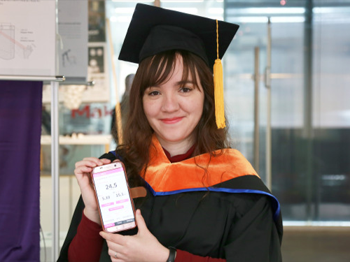 Kimchi Toolkit by Costa Rican Summa Cum Laude Helps Make the Best Flavor
(Maria Jose Reyes Castro with her kimchi toolkit application)
Every graduate feels a special attachment to their school, but for Maria Jose Reyes Castro who graduated summa cum laude in the Department of Industrial Design this year, KAIST will be remembered for more than just academics. She appreciates KAIST for not only giving her great professional opportunities, but also helping her find the love of her life.
During her master’s course, she completed an electronic kimchi toolkit, which optimizes kimchi’s flavor. Her kit uses a mobile application and smart sensor to find the fermentation level of kimchi by measuring its pH level, which is closely related to its fermentation. A user can set a desired fermentation level or salinity on the mobile application, and it provides the best date to serve it.
Under the guidance of Professor Daniel Saakes, she conducted research on developing a kimchi toolkit for beginners (Qualified Kimchi: Improving the experience of inexperienced kimchi makers by developing a monitoring toolkit for kimchi).
“I’ve seen many foreigners saying it’s quite difficult to make kimchi. So I chose to study kimchi to help people, especially those who are first-experienced making kimchi more easily,” she said. She got recipes from YouTube and studied fermentation through academic journals. She also asked kimchi experts to have a more profound understanding of it.
Extending her studies, she now works for a startup specializing in smart farms after starting last month. She conducts research on biology and applies it to designs that can be used practically in daily life.
Her tie with KAIST goes back to 2011 when she attended an international science camp in Germany. She met Sunghan Ro (’19 PhD in Nanoscience and Technology), a student from KAIST and now her husband. He recommended for her to enroll at KAIST because the school offers an outstanding education and research infrastructure along with support for foreign students.
At that time, Castro had just begun her first semester in electrical engineering at the University of Costa Rica, but she decided to apply to KAIST and seek a better opportunity in a new environment. One year later, she began her fresh start at KAIST in the fall semester of 2012.
Instead of choosing her original major, electrical engineering, she decided to pursue her studies in the Department of Industrial Design, because it is an interdisciplinary field where students get to study design while learning business models and making prototypes.
She said, “I felt encouraged by my professors and colleagues in my department to be creative and follow my passion. I never regret entering this major.”
When Castro was pursuing her master’s program in the same department, she became interested in interaction designs with food and biological designs by Professor Saakes, who is her advisor specializing in these areas.
After years of following her passion in design, she now graduates with academic honors in her department.
It is a bittersweet moment to close her journey at KAIST, but “I want to thank KAIST for the opportunity to change my life for the better. I also thank my parents for being supportive and encouraging me. I really appreciate the professors from the Department of Industrial Design who guided and shaped who I am,” she said.
Figure 1. The concept of the kimchi toolkit
Figure 2. The scenario of the kimchi toolkit
2019.02.19 View 6731
Kimchi Toolkit by Costa Rican Summa Cum Laude Helps Make the Best Flavor
(Maria Jose Reyes Castro with her kimchi toolkit application)
Every graduate feels a special attachment to their school, but for Maria Jose Reyes Castro who graduated summa cum laude in the Department of Industrial Design this year, KAIST will be remembered for more than just academics. She appreciates KAIST for not only giving her great professional opportunities, but also helping her find the love of her life.
During her master’s course, she completed an electronic kimchi toolkit, which optimizes kimchi’s flavor. Her kit uses a mobile application and smart sensor to find the fermentation level of kimchi by measuring its pH level, which is closely related to its fermentation. A user can set a desired fermentation level or salinity on the mobile application, and it provides the best date to serve it.
Under the guidance of Professor Daniel Saakes, she conducted research on developing a kimchi toolkit for beginners (Qualified Kimchi: Improving the experience of inexperienced kimchi makers by developing a monitoring toolkit for kimchi).
“I’ve seen many foreigners saying it’s quite difficult to make kimchi. So I chose to study kimchi to help people, especially those who are first-experienced making kimchi more easily,” she said. She got recipes from YouTube and studied fermentation through academic journals. She also asked kimchi experts to have a more profound understanding of it.
Extending her studies, she now works for a startup specializing in smart farms after starting last month. She conducts research on biology and applies it to designs that can be used practically in daily life.
Her tie with KAIST goes back to 2011 when she attended an international science camp in Germany. She met Sunghan Ro (’19 PhD in Nanoscience and Technology), a student from KAIST and now her husband. He recommended for her to enroll at KAIST because the school offers an outstanding education and research infrastructure along with support for foreign students.
At that time, Castro had just begun her first semester in electrical engineering at the University of Costa Rica, but she decided to apply to KAIST and seek a better opportunity in a new environment. One year later, she began her fresh start at KAIST in the fall semester of 2012.
Instead of choosing her original major, electrical engineering, she decided to pursue her studies in the Department of Industrial Design, because it is an interdisciplinary field where students get to study design while learning business models and making prototypes.
She said, “I felt encouraged by my professors and colleagues in my department to be creative and follow my passion. I never regret entering this major.”
When Castro was pursuing her master’s program in the same department, she became interested in interaction designs with food and biological designs by Professor Saakes, who is her advisor specializing in these areas.
After years of following her passion in design, she now graduates with academic honors in her department.
It is a bittersweet moment to close her journey at KAIST, but “I want to thank KAIST for the opportunity to change my life for the better. I also thank my parents for being supportive and encouraging me. I really appreciate the professors from the Department of Industrial Design who guided and shaped who I am,” she said.
Figure 1. The concept of the kimchi toolkit
Figure 2. The scenario of the kimchi toolkit
2019.02.19 View 6731 -
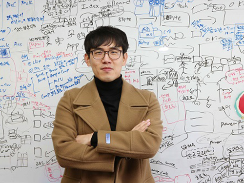 Professor Hojong Chang Wins the Best Paper Award at ISIITA 2018
Professor Hojong Chang from the KAIST Institute won the best paper award at the International Symposium on Innovation in Information Technology and Application (ISIITA) 2018.
ISIITA is a global networking symposium in which leading researchers in the field of information technology and applications gather to exchange knowledge on technological convergence.
Professor Chang won the prize for his paper, titled ‘A Study on the Measurement of Aptamer in Urine Using SiPM’.
This paper proposes using aptamer to measure and analyze the density of sodium and potassium contained in urine, allowing diseases to be diagnosed in advance.
Professor Chang said, “With a point-of-care test system that facilitates a quick diagnosis without extra processes, such as centrifugation, it is possible to get an early diagnosis and check infection in real time. Through generalizing this crucial technology, we expect to develop adequate technology for enhancing quality of life.
2018.02.12 View 10123
Professor Hojong Chang Wins the Best Paper Award at ISIITA 2018
Professor Hojong Chang from the KAIST Institute won the best paper award at the International Symposium on Innovation in Information Technology and Application (ISIITA) 2018.
ISIITA is a global networking symposium in which leading researchers in the field of information technology and applications gather to exchange knowledge on technological convergence.
Professor Chang won the prize for his paper, titled ‘A Study on the Measurement of Aptamer in Urine Using SiPM’.
This paper proposes using aptamer to measure and analyze the density of sodium and potassium contained in urine, allowing diseases to be diagnosed in advance.
Professor Chang said, “With a point-of-care test system that facilitates a quick diagnosis without extra processes, such as centrifugation, it is possible to get an early diagnosis and check infection in real time. Through generalizing this crucial technology, we expect to develop adequate technology for enhancing quality of life.
2018.02.12 View 10123