%50%72%69%6e%74%69%6e%67
-
 Direct Printing of Nanolasers, the Key to Optical Computing and Quantum Security
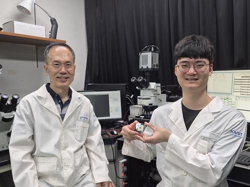
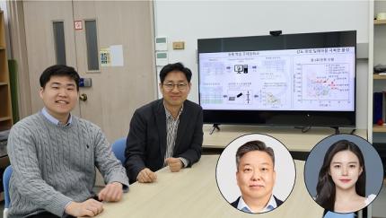
< (From left) Professor Ji Tae Kim (KAIST), Dr. Shiqi Hu (First Author, AI-based Intelligent Design-Manufacturing Integrated Research Group, KAIST-POSTECH), and Professor Junsuk Rho (POSTECH) >
In future high-tech industries, such as high-speed optical computing for massive AI, quantum cryptographic communication, and ultra-high-resolution augmented reality (AR) displays, nanolasers—which process information using light—are gaining significant attention as core components for next-generation semiconductors. A research team at our university has proposed a new manufacturing technology capable of high-density placement of nanolasers on semiconductor chips, which process information in spaces thinner than a human hair.
KAIST announced on January 6th that a joint research team, led by Professor Ji Tae Kim from the Department of Mechanical Engineering and Professor Junsuk Rho from POSTECH (President Seong-keun Kim), has developed an ultra-fine 3D printing technology capable of creating "vertical nanolasers," a key component for ultra-high-density optical integrated circuits.
Conventional semiconductor manufacturing methods, such as lithography, are effective for mass-producing identical structures but face limitations: the processes are complex and costly, making it difficult to freely change the shape or position of devices. Furthermore, most existing lasers are built as horizontal structures lying flat on a substrate, which consumes significant space and suffers from reduced efficiency due to light leakage into the substrate.
To solve these issues, the research team developed a new 3D printing method to vertically stack perovskite, a next-generation semiconductor material that generates light efficiently. This technology, known as "ultra-fine electrohydrodynamic 3D printing," uses electrical voltage to precisely control invisible ink droplets at the attoliter scale ($10^{-18}$ L).
Through this method, the team successfully printed pillar-shaped nanostructures—much thinner than a human hair—directly and vertically at desired locations without the need for complex subtractive processes (carving material away).
The core of this technology lies in significantly increasing laser efficiency by making the surface of the printed perovskite nanostructures extremely smooth. By combining the printing process with gas-phase crystallization control technology, the team achieved high-quality structures with nearly single-crystalline alignment. As a result, they were able to realize high-efficiency vertical nanolasers that operate stably with minimal light loss.
Additionally, the team demonstrated that the color of the emitted laser light could be precisely tuned by adjusting the height of the nanostructures. Utilizing this, they created laser security patterns invisible to the naked eye—identifiable only with specialized equipment—confirming the potential for commercialization in anti-counterfeiting technology.
< 3D Printing of Perovskite Nanolasers >
Professor Jitae Kim stated, "This technology allows for the direct, high-density implementation of optical computing semiconductors on a chip without complex processing. It will accelerate the commercialization of ultra-high-speed optical computing and next-generation security technologies."
The research results, with Dr. Shiqi Hu from the Department of Mechanical Engineering as the first author, were published online on December 6, 2025, in ACS Nano, an international prestigious journal in the field of nanoscience.
Paper Title: Nanoprinting with Crystal Engineering for Perovskite Lasers
DOI: https://doi.org/10.1021/acsnano.5c16906
This research was conducted with support from the Ministry of Science and ICT’s Excellent Young Researcher Program (RS-2025-00556379), the Mid-career Researcher Support Program (RS-2024-00356928), and the InnoCORE AI-based Intelligent Design-Manufacturing Integrated Research Group (N10250154).
2026.01.06 View 2265
Direct Printing of Nanolasers, the Key to Optical Computing and Quantum Security
< (From left) Professor Ji Tae Kim (KAIST), Dr. Shiqi Hu (First Author, AI-based Intelligent Design-Manufacturing Integrated Research Group, KAIST-POSTECH), and Professor Junsuk Rho (POSTECH) >
In future high-tech industries, such as high-speed optical computing for massive AI, quantum cryptographic communication, and ultra-high-resolution augmented reality (AR) displays, nanolasers—which process information using light—are gaining significant attention as core components for next-generation semiconductors. A research team at our university has proposed a new manufacturing technology capable of high-density placement of nanolasers on semiconductor chips, which process information in spaces thinner than a human hair.
KAIST announced on January 6th that a joint research team, led by Professor Ji Tae Kim from the Department of Mechanical Engineering and Professor Junsuk Rho from POSTECH (President Seong-keun Kim), has developed an ultra-fine 3D printing technology capable of creating "vertical nanolasers," a key component for ultra-high-density optical integrated circuits.
Conventional semiconductor manufacturing methods, such as lithography, are effective for mass-producing identical structures but face limitations: the processes are complex and costly, making it difficult to freely change the shape or position of devices. Furthermore, most existing lasers are built as horizontal structures lying flat on a substrate, which consumes significant space and suffers from reduced efficiency due to light leakage into the substrate.
To solve these issues, the research team developed a new 3D printing method to vertically stack perovskite, a next-generation semiconductor material that generates light efficiently. This technology, known as "ultra-fine electrohydrodynamic 3D printing," uses electrical voltage to precisely control invisible ink droplets at the attoliter scale ($10^{-18}$ L).
Through this method, the team successfully printed pillar-shaped nanostructures—much thinner than a human hair—directly and vertically at desired locations without the need for complex subtractive processes (carving material away).
The core of this technology lies in significantly increasing laser efficiency by making the surface of the printed perovskite nanostructures extremely smooth. By combining the printing process with gas-phase crystallization control technology, the team achieved high-quality structures with nearly single-crystalline alignment. As a result, they were able to realize high-efficiency vertical nanolasers that operate stably with minimal light loss.
Additionally, the team demonstrated that the color of the emitted laser light could be precisely tuned by adjusting the height of the nanostructures. Utilizing this, they created laser security patterns invisible to the naked eye—identifiable only with specialized equipment—confirming the potential for commercialization in anti-counterfeiting technology.
< 3D Printing of Perovskite Nanolasers >
Professor Jitae Kim stated, "This technology allows for the direct, high-density implementation of optical computing semiconductors on a chip without complex processing. It will accelerate the commercialization of ultra-high-speed optical computing and next-generation security technologies."
The research results, with Dr. Shiqi Hu from the Department of Mechanical Engineering as the first author, were published online on December 6, 2025, in ACS Nano, an international prestigious journal in the field of nanoscience.
Paper Title: Nanoprinting with Crystal Engineering for Perovskite Lasers
DOI: https://doi.org/10.1021/acsnano.5c16906
This research was conducted with support from the Ministry of Science and ICT’s Excellent Young Researcher Program (RS-2025-00556379), the Mid-career Researcher Support Program (RS-2024-00356928), and the InnoCORE AI-based Intelligent Design-Manufacturing Integrated Research Group (N10250154).
2026.01.06 View 2265 -
 KAIST Develops Room-Temperature 3D Printing Technology for ‘Electronic Eyes’—Miniaturized Infrared Sensors
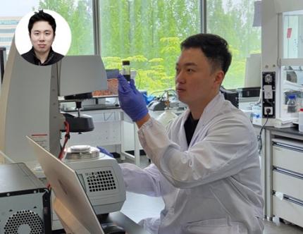
<(From Left) Professor Ji Tae Kim of the Department of Mechanical Engineering, Professor Soong Ju Oh of Korea University and Professor Tianshuo Zhao of the University of Hong Kong>
The “electronic eyes” technology that can recognize objects even in darkness has taken a step forward. Infrared sensors, which act as the “seeing” component in devices such as LiDAR for autonomous vehicles, 3D face recognition systems in smartphones, and wearable healthcare devices, are regarded as key components in next-generation electronics. Now, a research team at KAIST and their collaborators have developed the world’s first room-temperature 3D printing technology that can fabricate miniature infrared sensors in any desired shape and size.
KAIST (President Kwang Hyung Lee) announced on the 3rd of November that the research team led by Professor Ji Tae Kim of the Department of Mechanical Engineering, in collaboration with Professor Soong Ju Oh of Korea University and Professor Tianshuo Zhao of the University of Hong Kong, has developed a 3D printing technique capable of fabricating ultra-small infrared sensors—smaller than 10 micrometers (µm)—in customized shapes and sizes at room temperature.
Infrared sensors convert invisible infrared signals into electrical signals and serve as essential components in realizing future electronic technologies such as robotic vision. Accordingly, miniaturization, weight reduction, and flexible form-factor design have become increasingly important.
Conventional semiconductor fabrication processes were well suited for mass production but struggled to adapt flexibly to rapidly changing technological demands. They also required high-temperature processing, which limited material choices and consumed large amounts of energy.
To overcome these challenges, the research team developed an ultra-precise 3D printing process that uses metal, semiconductor, and insulator materials in the form of liquid nanocrystal inks, stacking them layer by layer within a single printing platform.
This method enables direct fabrication of core components of infrared sensors at room temperature, allowing for the realization of customized miniature sensors of various shapes and sizes.
Particularly, the researchers achieved excellent electrical performance without the need for high-temperature annealing by applying a “ligand-exchange” process, where insulating molecules on the surface of nanoparticles are replaced with conductive ones.
As a result, the team successfully fabricated ultra-small infrared sensors measuring less than one-tenth the thickness of a human hair (under 10 µm).
<Figure 1. 3D printing of infrared sensors.a. Room-temperature printing process for the electrodes and photoactive layer that make up the infrared sensor.b. Structure and chemical composition of the printed infrared microsensor. c.Printed infrared sensor micropixel array.>
Professor Ji Tae Kim commented, “The developed 3D printing technology not only advances the miniaturization and lightweight design of infrared sensors but also paves the way for the creation of innovative new form-factor products that were previously unimaginable. Moreover, by reducing the massive energy consumption associated with high-temperature processes, this approach can lower production costs and enable eco-friendly manufacturing—contributing to the sustainable development of the infrared sensor industry.”
The research results were published online in Nature Communications on October 16, 2025, under the title “Ligand-exchange-assisted printing of colloidal nanocrystals to enable all-printed sub-micron optoelectronics” (DOI: https://doi.org/10.1038/s41467-025-64596-4).
This research was supported by the Ministry of Science and ICT of Korea through the Excellent Young Researcher Program (RS−2025−00556379), the National Strategic Technology Material Development Program (RS−2024−00407084), and the International Cooperation Research Program for Original Technology Development (RS−2024−00438059).
2025.11.03 View 5199
KAIST Develops Room-Temperature 3D Printing Technology for ‘Electronic Eyes’—Miniaturized Infrared Sensors
<(From Left) Professor Ji Tae Kim of the Department of Mechanical Engineering, Professor Soong Ju Oh of Korea University and Professor Tianshuo Zhao of the University of Hong Kong>
The “electronic eyes” technology that can recognize objects even in darkness has taken a step forward. Infrared sensors, which act as the “seeing” component in devices such as LiDAR for autonomous vehicles, 3D face recognition systems in smartphones, and wearable healthcare devices, are regarded as key components in next-generation electronics. Now, a research team at KAIST and their collaborators have developed the world’s first room-temperature 3D printing technology that can fabricate miniature infrared sensors in any desired shape and size.
KAIST (President Kwang Hyung Lee) announced on the 3rd of November that the research team led by Professor Ji Tae Kim of the Department of Mechanical Engineering, in collaboration with Professor Soong Ju Oh of Korea University and Professor Tianshuo Zhao of the University of Hong Kong, has developed a 3D printing technique capable of fabricating ultra-small infrared sensors—smaller than 10 micrometers (µm)—in customized shapes and sizes at room temperature.
Infrared sensors convert invisible infrared signals into electrical signals and serve as essential components in realizing future electronic technologies such as robotic vision. Accordingly, miniaturization, weight reduction, and flexible form-factor design have become increasingly important.
Conventional semiconductor fabrication processes were well suited for mass production but struggled to adapt flexibly to rapidly changing technological demands. They also required high-temperature processing, which limited material choices and consumed large amounts of energy.
To overcome these challenges, the research team developed an ultra-precise 3D printing process that uses metal, semiconductor, and insulator materials in the form of liquid nanocrystal inks, stacking them layer by layer within a single printing platform.
This method enables direct fabrication of core components of infrared sensors at room temperature, allowing for the realization of customized miniature sensors of various shapes and sizes.
Particularly, the researchers achieved excellent electrical performance without the need for high-temperature annealing by applying a “ligand-exchange” process, where insulating molecules on the surface of nanoparticles are replaced with conductive ones.
As a result, the team successfully fabricated ultra-small infrared sensors measuring less than one-tenth the thickness of a human hair (under 10 µm).
<Figure 1. 3D printing of infrared sensors.a. Room-temperature printing process for the electrodes and photoactive layer that make up the infrared sensor.b. Structure and chemical composition of the printed infrared microsensor. c.Printed infrared sensor micropixel array.>
Professor Ji Tae Kim commented, “The developed 3D printing technology not only advances the miniaturization and lightweight design of infrared sensors but also paves the way for the creation of innovative new form-factor products that were previously unimaginable. Moreover, by reducing the massive energy consumption associated with high-temperature processes, this approach can lower production costs and enable eco-friendly manufacturing—contributing to the sustainable development of the infrared sensor industry.”
The research results were published online in Nature Communications on October 16, 2025, under the title “Ligand-exchange-assisted printing of colloidal nanocrystals to enable all-printed sub-micron optoelectronics” (DOI: https://doi.org/10.1038/s41467-025-64596-4).
This research was supported by the Ministry of Science and ICT of Korea through the Excellent Young Researcher Program (RS−2025−00556379), the National Strategic Technology Material Development Program (RS−2024−00407084), and the International Cooperation Research Program for Original Technology Development (RS−2024−00438059).
2025.11.03 View 5199 -
 3D Printing Becomes Stronger and More Economical with Light and AI
<(Front) Ph.D. candidate Jisoo Nam, (Back row, from left) Ph.D. candidate Boxin Chen, Professor Miso Kim>
Photocurable 3D printing, widely used for everything from dental treatments to complex prototype manufacturing, is fast and precise but has the limitation of being fragile and easily broken by impact. A KAIST research team has developed a new technology to overcome this weakness, paving the way for the more robust and economical production of everything from medical implants to precision machine parts.
KAIST (President Kwang Hyung Lee) announced on the 29th that Professor Miso Kim's research team in the Department of Mechanical Engineering has developed a new technology that fundamentally resolves the durability limitations of photocurable 3D printing.
Digital Light Processing (DLP)-based 3D printing is a technique that uses light to solidify liquid resin (polymer) to rapidly manufacture precise structures, used in various fields such as dentistry and precision machinery. While traditional injection molding offers excellent durability, it requires significant time and cost for mold fabrication. In contrast, photocurable 3D printing allows for flexible shape realization but has a durability drawback.
Professor Kim's team solved this problem by combining two key elements:
A new photocurable resin material that absorbs shock and vibration while allowing for a wide range of properties from rubber to plastic.
A machine learning-based design technology that automatically assigns optimal strength to each part of the structure.
<Figure 1. Schematic of a new manufacturing technology for high-durability photocurable 3D printing using light-controlled gradient structures. This approach integrates the development of stiffness-controllable viscoelastic polyurethane acrylate (PUA) materials, machine learning-based property gradient optimization, and grayscale DLP 3D printing. The technology enhances damping performance and alleviates stress concentration, providing an integrated solution for high reliability, durability, and customized manufacturing. It demonstrates potential applications in structural components subjected to repetitive loads such as joints, automotive interior parts, and precision machinery components>
The research team developed a Polyurethane Acrylate (PUA) material incorporating dynamic bonds, which significantly increases shock and vibration absorption capability compared to existing materials. Furthermore, they successfully applied 'grayscale DLP' technology, which controls the light intensity to achieve different strengths from a single resin composition, thereby assigning customized strength to specific areas within the structure. This concept is inspired by the harmonious and different roles played by bone and cartilage in the human body.
A machine learning algorithm automatically proposes the optimal strength distribution by analyzing the structure and load conditions. This organically connects material development and structural design, enabling customized strength distribution.
The economic efficiency is also noteworthy. Previously, expensive 'multi-material printing' technology was required to achieve diverse material properties, but this new technology yields the same effect with a single material and a single process, significantly reducing production costs. It eliminates the need for complex equipment or material management, and the AI-based structural optimization shortens research and development time and product design costs.
Professor Miso Kim explained, "This technology simultaneously expands the degrees of freedom in material properties and structural design. Patient-specific implants will become more durable and comfortable, and precision machine parts can be manufactured more robustly." She added, "The fact that it secures economic viability by realizing various strengths with a single material and single process is highly significant," and "We anticipate its utilization across various industrial fields such as biomedical, aerospace, and robotics."
The research was spearheaded by Professor Miso Kim's team at the KAIST Department of Mechanical Engineering, with Ph.D. candidate Jisoo Nam as the first author. Boxin Chen, a student from Sungkyunkwan University, also contributed to the collaborative research. The findings were published online on July 16 in the world-renowned journal in materials science, Advanced Materials (IF 26.8). Recognizing the research's excellence, it was also selected for the journal's Frontispiece.
Paper Title: Machine Learning-Driven Grayscale Digital Light Processing for Mechanically Robust 3D-Printed Gradient Materials
DOI: 10.1002/adma.202504075
The achievements of this research have brought Professor Miso Kim significant international attention, as she simultaneously received the 'Wiley Rising Star Award' and the 'Wiley Women in Materials Science Award' in July 2025, hosted by the international academic publisher Wiley.
The Wiley Rising Star Award is given to emerging researchers with the potential for academic leadership, and the Wiley Women in Materials Science Award is a prestigious honor established to celebrate outstanding female scientists in the field of materials science.
<Figure 2. Frontispiece image (scheduled for Issue 42). Multi-property structure fabricated using a photocurable 3D printer. By varying the projector light intensity by location, stronger light creates rigid regions while weaker light forms flexible ones. AI designs an optimized pattern for the structural shape to prevent fracture and reinforce the overall strength.>
This research was supported by the National Research Foundation of Korea (NRF) grants funded by the Korean government (MSIT) (Nos. NRF-2021R1A2C2095767, RS-2023-00254689, and RS-2024-00433654).
2025.09.30 View 3589
3D Printing Becomes Stronger and More Economical with Light and AI
<(Front) Ph.D. candidate Jisoo Nam, (Back row, from left) Ph.D. candidate Boxin Chen, Professor Miso Kim>
Photocurable 3D printing, widely used for everything from dental treatments to complex prototype manufacturing, is fast and precise but has the limitation of being fragile and easily broken by impact. A KAIST research team has developed a new technology to overcome this weakness, paving the way for the more robust and economical production of everything from medical implants to precision machine parts.
KAIST (President Kwang Hyung Lee) announced on the 29th that Professor Miso Kim's research team in the Department of Mechanical Engineering has developed a new technology that fundamentally resolves the durability limitations of photocurable 3D printing.
Digital Light Processing (DLP)-based 3D printing is a technique that uses light to solidify liquid resin (polymer) to rapidly manufacture precise structures, used in various fields such as dentistry and precision machinery. While traditional injection molding offers excellent durability, it requires significant time and cost for mold fabrication. In contrast, photocurable 3D printing allows for flexible shape realization but has a durability drawback.
Professor Kim's team solved this problem by combining two key elements:
A new photocurable resin material that absorbs shock and vibration while allowing for a wide range of properties from rubber to plastic.
A machine learning-based design technology that automatically assigns optimal strength to each part of the structure.
<Figure 1. Schematic of a new manufacturing technology for high-durability photocurable 3D printing using light-controlled gradient structures. This approach integrates the development of stiffness-controllable viscoelastic polyurethane acrylate (PUA) materials, machine learning-based property gradient optimization, and grayscale DLP 3D printing. The technology enhances damping performance and alleviates stress concentration, providing an integrated solution for high reliability, durability, and customized manufacturing. It demonstrates potential applications in structural components subjected to repetitive loads such as joints, automotive interior parts, and precision machinery components>
The research team developed a Polyurethane Acrylate (PUA) material incorporating dynamic bonds, which significantly increases shock and vibration absorption capability compared to existing materials. Furthermore, they successfully applied 'grayscale DLP' technology, which controls the light intensity to achieve different strengths from a single resin composition, thereby assigning customized strength to specific areas within the structure. This concept is inspired by the harmonious and different roles played by bone and cartilage in the human body.
A machine learning algorithm automatically proposes the optimal strength distribution by analyzing the structure and load conditions. This organically connects material development and structural design, enabling customized strength distribution.
The economic efficiency is also noteworthy. Previously, expensive 'multi-material printing' technology was required to achieve diverse material properties, but this new technology yields the same effect with a single material and a single process, significantly reducing production costs. It eliminates the need for complex equipment or material management, and the AI-based structural optimization shortens research and development time and product design costs.
Professor Miso Kim explained, "This technology simultaneously expands the degrees of freedom in material properties and structural design. Patient-specific implants will become more durable and comfortable, and precision machine parts can be manufactured more robustly." She added, "The fact that it secures economic viability by realizing various strengths with a single material and single process is highly significant," and "We anticipate its utilization across various industrial fields such as biomedical, aerospace, and robotics."
The research was spearheaded by Professor Miso Kim's team at the KAIST Department of Mechanical Engineering, with Ph.D. candidate Jisoo Nam as the first author. Boxin Chen, a student from Sungkyunkwan University, also contributed to the collaborative research. The findings were published online on July 16 in the world-renowned journal in materials science, Advanced Materials (IF 26.8). Recognizing the research's excellence, it was also selected for the journal's Frontispiece.
Paper Title: Machine Learning-Driven Grayscale Digital Light Processing for Mechanically Robust 3D-Printed Gradient Materials
DOI: 10.1002/adma.202504075
The achievements of this research have brought Professor Miso Kim significant international attention, as she simultaneously received the 'Wiley Rising Star Award' and the 'Wiley Women in Materials Science Award' in July 2025, hosted by the international academic publisher Wiley.
The Wiley Rising Star Award is given to emerging researchers with the potential for academic leadership, and the Wiley Women in Materials Science Award is a prestigious honor established to celebrate outstanding female scientists in the field of materials science.
<Figure 2. Frontispiece image (scheduled for Issue 42). Multi-property structure fabricated using a photocurable 3D printer. By varying the projector light intensity by location, stronger light creates rigid regions while weaker light forms flexible ones. AI designs an optimized pattern for the structural shape to prevent fracture and reinforce the overall strength.>
This research was supported by the National Research Foundation of Korea (NRF) grants funded by the Korean government (MSIT) (Nos. NRF-2021R1A2C2095767, RS-2023-00254689, and RS-2024-00433654).
2025.09.30 View 3589 -
 KAIST Successfully Implements 3D Brain-Mimicking Platform with 6x Higher Precision
<(From left) Dr. Dongjo Yoon, Professor Je-Kyun Park from the Department of Bio and Brain Engineering, (upper right) Professor Yoonkey Nam, Dr. Soo Jee Kim>
Existing three-dimensional (3D) neuronal culture technology has limitations in brain research due to the difficulty of precisely replicating the brain's complex multilayered structure and the lack of a platform that can simultaneously analyze both structure and function. A KAIST research team has successfully developed an integrated platform that can implement brain-like layered neuronal structures using 3D printing technology and precisely measure neuronal activity within them.
KAIST (President Kwang Hyung Lee) announced on the 16th of July that a joint research team led by Professors Je-Kyun Park and Yoonkey Nam from the Department of Bio and Brain Engineering has developed an integrated platform capable of fabricating high-resolution 3D multilayer neuronal networks using low-viscosity natural hydrogels with mechanical properties similar to brain tissue, and simultaneously analyzing their structural and functional connectivity.
Conventional bioprinting technology uses high-viscosity bioinks for structural stability, but this limits neuronal proliferation and neurite growth. Conversely, neural cell-friendly low-viscosity hydrogels are difficult to precisely pattern, leading to a fundamental trade-off between structural stability and biological function. The research team completed a sophisticated and stable brain-mimicking platform by combining three key technologies that enable the precise creation of brain structure with dilute gels, accurate alignment between layers, and simultaneous observation of neuronal activity.
The three core technologies are: ▲ 'Capillary Pinning Effect' technology, which enables the dilute gel (hydrogel) to adhere firmly to a stainless steel mesh (micromesh) to prevent it from flowing, thereby reproducing brain structures with six times greater precision (resolution of 500 μm or less) than conventional methods; ▲ the '3D Printing Aligner,' a cylindrical design that ensures the printed layers are precisely stacked without misalignment, guaranteeing the accurate assembly of multilayer structures and stable integration with microelectrode chips; and ▲ 'Dual-mode Analysis System' technology, which simultaneously measures electrical signals from below and observes cell activity with light (calcium imaging) from above, allowing for the simultaneous verification of the functional operation of interlayer connections through multiple methods.
< Figure 1. Platform integrating brain-structure-mimicking neural network model construction and functional measurement technology>
The research team successfully implemented a three-layered mini-brain structure using 3D printing with a fibrin hydrogel, which has elastic properties similar to those of the brain, and experimentally verified the process of actual neural cells transmitting and receiving signals within it.
Cortical neurons were placed in the upper and lower layers, while the middle layer was left empty but designed to allow neurons to penetrate and connect through it. Electrical signals were measured from the lower layer using a microsensor (electrode chip), and cell activity was observed from the upper layer using light (calcium imaging). The results showed that when electrical stimulation was applied, neural cells in both upper and lower layers responded simultaneously. When a synapse-blocking agent (synaptic blocker) was introduced, the response decreased, proving that the neural cells were genuinely connected and transmitting signals.
Professor Je-Kyun Park of KAIST explained, "This research is a joint development achievement of an integrated platform that can simultaneously reproduce the complex multilayered structure and function of brain tissue. Compared to existing technologies where signal measurement was impossible for more than 14 days, this platform maintains a stable microelectrode chip interface for over 27 days, allowing the real-time analysis of structure-function relationships. It can be utilized in various brain research fields such as neurological disease modeling, brain function research, neurotoxicity assessment, and neuroprotective drug screening in the future."
The research, in which Dr. Soo Jee Kim and Dr. Dongjo Yoon from KAIST's Department of Bio and Brain Engineering participated as co-first authors, was published online in the international journal 'Biosensors and Bioelectronics' on June 11, 2025.
※Paper: Hybrid biofabrication of multilayered 3D neuronal networks with structural and functional interlayer connectivity
※DOI: https://doi.org/10.1016/j.bios.2025.117688
2025.07.16 View 4378
KAIST Successfully Implements 3D Brain-Mimicking Platform with 6x Higher Precision
<(From left) Dr. Dongjo Yoon, Professor Je-Kyun Park from the Department of Bio and Brain Engineering, (upper right) Professor Yoonkey Nam, Dr. Soo Jee Kim>
Existing three-dimensional (3D) neuronal culture technology has limitations in brain research due to the difficulty of precisely replicating the brain's complex multilayered structure and the lack of a platform that can simultaneously analyze both structure and function. A KAIST research team has successfully developed an integrated platform that can implement brain-like layered neuronal structures using 3D printing technology and precisely measure neuronal activity within them.
KAIST (President Kwang Hyung Lee) announced on the 16th of July that a joint research team led by Professors Je-Kyun Park and Yoonkey Nam from the Department of Bio and Brain Engineering has developed an integrated platform capable of fabricating high-resolution 3D multilayer neuronal networks using low-viscosity natural hydrogels with mechanical properties similar to brain tissue, and simultaneously analyzing their structural and functional connectivity.
Conventional bioprinting technology uses high-viscosity bioinks for structural stability, but this limits neuronal proliferation and neurite growth. Conversely, neural cell-friendly low-viscosity hydrogels are difficult to precisely pattern, leading to a fundamental trade-off between structural stability and biological function. The research team completed a sophisticated and stable brain-mimicking platform by combining three key technologies that enable the precise creation of brain structure with dilute gels, accurate alignment between layers, and simultaneous observation of neuronal activity.
The three core technologies are: ▲ 'Capillary Pinning Effect' technology, which enables the dilute gel (hydrogel) to adhere firmly to a stainless steel mesh (micromesh) to prevent it from flowing, thereby reproducing brain structures with six times greater precision (resolution of 500 μm or less) than conventional methods; ▲ the '3D Printing Aligner,' a cylindrical design that ensures the printed layers are precisely stacked without misalignment, guaranteeing the accurate assembly of multilayer structures and stable integration with microelectrode chips; and ▲ 'Dual-mode Analysis System' technology, which simultaneously measures electrical signals from below and observes cell activity with light (calcium imaging) from above, allowing for the simultaneous verification of the functional operation of interlayer connections through multiple methods.
< Figure 1. Platform integrating brain-structure-mimicking neural network model construction and functional measurement technology>
The research team successfully implemented a three-layered mini-brain structure using 3D printing with a fibrin hydrogel, which has elastic properties similar to those of the brain, and experimentally verified the process of actual neural cells transmitting and receiving signals within it.
Cortical neurons were placed in the upper and lower layers, while the middle layer was left empty but designed to allow neurons to penetrate and connect through it. Electrical signals were measured from the lower layer using a microsensor (electrode chip), and cell activity was observed from the upper layer using light (calcium imaging). The results showed that when electrical stimulation was applied, neural cells in both upper and lower layers responded simultaneously. When a synapse-blocking agent (synaptic blocker) was introduced, the response decreased, proving that the neural cells were genuinely connected and transmitting signals.
Professor Je-Kyun Park of KAIST explained, "This research is a joint development achievement of an integrated platform that can simultaneously reproduce the complex multilayered structure and function of brain tissue. Compared to existing technologies where signal measurement was impossible for more than 14 days, this platform maintains a stable microelectrode chip interface for over 27 days, allowing the real-time analysis of structure-function relationships. It can be utilized in various brain research fields such as neurological disease modeling, brain function research, neurotoxicity assessment, and neuroprotective drug screening in the future."
The research, in which Dr. Soo Jee Kim and Dr. Dongjo Yoon from KAIST's Department of Bio and Brain Engineering participated as co-first authors, was published online in the international journal 'Biosensors and Bioelectronics' on June 11, 2025.
※Paper: Hybrid biofabrication of multilayered 3D neuronal networks with structural and functional interlayer connectivity
※DOI: https://doi.org/10.1016/j.bios.2025.117688
2025.07.16 View 4378 -
 Military Combatants Usher in an Era of Personalized Training with New Materials
< Photo 1. (From left) Professor Steve Park of Materials Science and Engineering, Kyusoon Pak, Ph.D. Candidate (Army Major) >
Traditional military training often relies on standardized methods, which has limited the provision of optimized training tailored to individual combatants' characteristics or specific combat situations. To address this, our research team developed an e-textile platform, securing core technology that can reflect the unique traits of individual combatants and various combat scenarios. This technology has proven robust enough for battlefield use and is economical enough for widespread distribution to a large number of troops.
On June 25th, Professor Steve Park's research team at KAIST's Department of Materials Science and Engineering announced the development of a flexible, wearable electronic textile (E-textile) platform using an innovative technology that 'draws' electronic circuits directly onto fabric.
The wearable e-textile platform developed by the research team combines 3D printing technology with new materials engineering design to directly print flexible and highly durable sensors and electrodes onto textile substrates. This enables the collection of precise movement and human body data from individual combatants, which can then be used to propose customized training models.
Existing e-textile fabrication methods were often complex or limited in their ability to provide personalized customization. To overcome these challenges, the research team adopted an additive manufacturing technology called 'Direct Ink Writing (DIW)' 3D printing.
< Figure 1. Schematic diagram of e-textile manufactured with Direct Ink Writing (DIW) printing technology on various textiles, including combat uniforms >
This technology involves directly dispensing and printing special ink, which functions as sensors and electrodes, onto textile substrates in desired patterns. This allows for flexible implementation of various designs without the complex process of mask fabrication. This is expected to be an effective technology that can be easily supplied to hundreds of thousands of military personnel.
The core of this technology lies in the development of high-performance functional inks based on advanced materials engineering design. The research team combined styrene-butadiene-styrene (SBS) polymer, which provides flexibility, with multi-walled carbon nanotubes (MWCNT) for electrical conductivity. They developed a tensile/bending sensor ink that can stretch up to 102% and maintain stable performance even after 10,000 repetitive tests. This means that accurate data can be consistently obtained even during the strenuous movements of combatants.
< Figure 2. Measurement of human movement and breathing patterns using e-textile >
Furthermore, new material technology was applied to implement 'interconnect electrodes' that electrically connect the upper and lower layers of the fabric. The team developed an electrode ink combining silver (Ag) flakes with rigid polystyrene (PS) polymer, precisely controlling the impregnation level (how much the ink penetrates the fabric) to effectively connect both sides or multiple layers of the fabric. This secures the technology for producing multi-layered wearable electronic systems integrating sensors and electrodes.
< Figure 3. Experimental results of recognizing unknown objects after machine learning six objects using a smart glove >
The research team proved the platform's performance through actual human movement monitoring experiments. They printed the developed e-textile on major joint areas of clothing (shoulders, elbows, knees) and measured movements and posture changes during various exercises such as running, jumping jacks, and push-ups in real-time.
Additionally, they demonstrated the potential for applications such as monitoring breathing patterns using a smart mask and recognizing objects through machine learning and perceiving complex tactile information by printing multiple sensors and electrodes on gloves. These results show that the developed e-textile platform is effective in precisely understanding the movement dynamics of combatants.
This research is an important example demonstrating how cutting-edge new material technology can contribute to the advancement of the defense sector. Major Kyusoon Pak of the Army, who participated in this research, considered required objectives such as military applicability and economic feasibility for practical distribution from the research design stage.
< Figure 4. Experimental results showing that a multi-layered e-textile glove connected with interconnect electrodes can measure tensile/bending signals and pressure signals at a single point >
Major Pak stated, "Our military is currently facing both a crisis and an opportunity due to the decrease in military personnel resources caused by the demographic cliff and the advancement of science and technology. Also, respect for life in the battlefield is emerging as a significant issue. This research aims to secure original technology that can provide customized training according to military branch/duty and type of combat, thereby enhancing the combat power and ensuring the survivability of our soldiers."
He added, "I hope this research will be evaluated as a case that achieved both scientific contribution and military applicability."
This research, where Kyusoon Pak, Ph.D. Candidate (Army Major) from KAIST's Department of Materials Science and Engineering, participated as the first author and Professor Steve Park supervised, was published on May 27, 2025, in `npj Flexible Electronics (top 1.8% in JCR field)', an international academic journal in the electrical, electronic, and materials engineering fields.
* Paper Title: Fabrication of Multifunctional Wearable Interconnect E-textile Platform Using Direct Ink Writing (DIW) 3D Printing
* DOI: https://doi.org/10.1038/s41528-025-00414-7
This research was supported by the Ministry of Trade, Industry and Energy and the National Research Foundation of Korea.
2025.06.25 View 7604
Military Combatants Usher in an Era of Personalized Training with New Materials
< Photo 1. (From left) Professor Steve Park of Materials Science and Engineering, Kyusoon Pak, Ph.D. Candidate (Army Major) >
Traditional military training often relies on standardized methods, which has limited the provision of optimized training tailored to individual combatants' characteristics or specific combat situations. To address this, our research team developed an e-textile platform, securing core technology that can reflect the unique traits of individual combatants and various combat scenarios. This technology has proven robust enough for battlefield use and is economical enough for widespread distribution to a large number of troops.
On June 25th, Professor Steve Park's research team at KAIST's Department of Materials Science and Engineering announced the development of a flexible, wearable electronic textile (E-textile) platform using an innovative technology that 'draws' electronic circuits directly onto fabric.
The wearable e-textile platform developed by the research team combines 3D printing technology with new materials engineering design to directly print flexible and highly durable sensors and electrodes onto textile substrates. This enables the collection of precise movement and human body data from individual combatants, which can then be used to propose customized training models.
Existing e-textile fabrication methods were often complex or limited in their ability to provide personalized customization. To overcome these challenges, the research team adopted an additive manufacturing technology called 'Direct Ink Writing (DIW)' 3D printing.
< Figure 1. Schematic diagram of e-textile manufactured with Direct Ink Writing (DIW) printing technology on various textiles, including combat uniforms >
This technology involves directly dispensing and printing special ink, which functions as sensors and electrodes, onto textile substrates in desired patterns. This allows for flexible implementation of various designs without the complex process of mask fabrication. This is expected to be an effective technology that can be easily supplied to hundreds of thousands of military personnel.
The core of this technology lies in the development of high-performance functional inks based on advanced materials engineering design. The research team combined styrene-butadiene-styrene (SBS) polymer, which provides flexibility, with multi-walled carbon nanotubes (MWCNT) for electrical conductivity. They developed a tensile/bending sensor ink that can stretch up to 102% and maintain stable performance even after 10,000 repetitive tests. This means that accurate data can be consistently obtained even during the strenuous movements of combatants.
< Figure 2. Measurement of human movement and breathing patterns using e-textile >
Furthermore, new material technology was applied to implement 'interconnect electrodes' that electrically connect the upper and lower layers of the fabric. The team developed an electrode ink combining silver (Ag) flakes with rigid polystyrene (PS) polymer, precisely controlling the impregnation level (how much the ink penetrates the fabric) to effectively connect both sides or multiple layers of the fabric. This secures the technology for producing multi-layered wearable electronic systems integrating sensors and electrodes.
< Figure 3. Experimental results of recognizing unknown objects after machine learning six objects using a smart glove >
The research team proved the platform's performance through actual human movement monitoring experiments. They printed the developed e-textile on major joint areas of clothing (shoulders, elbows, knees) and measured movements and posture changes during various exercises such as running, jumping jacks, and push-ups in real-time.
Additionally, they demonstrated the potential for applications such as monitoring breathing patterns using a smart mask and recognizing objects through machine learning and perceiving complex tactile information by printing multiple sensors and electrodes on gloves. These results show that the developed e-textile platform is effective in precisely understanding the movement dynamics of combatants.
This research is an important example demonstrating how cutting-edge new material technology can contribute to the advancement of the defense sector. Major Kyusoon Pak of the Army, who participated in this research, considered required objectives such as military applicability and economic feasibility for practical distribution from the research design stage.
< Figure 4. Experimental results showing that a multi-layered e-textile glove connected with interconnect electrodes can measure tensile/bending signals and pressure signals at a single point >
Major Pak stated, "Our military is currently facing both a crisis and an opportunity due to the decrease in military personnel resources caused by the demographic cliff and the advancement of science and technology. Also, respect for life in the battlefield is emerging as a significant issue. This research aims to secure original technology that can provide customized training according to military branch/duty and type of combat, thereby enhancing the combat power and ensuring the survivability of our soldiers."
He added, "I hope this research will be evaluated as a case that achieved both scientific contribution and military applicability."
This research, where Kyusoon Pak, Ph.D. Candidate (Army Major) from KAIST's Department of Materials Science and Engineering, participated as the first author and Professor Steve Park supervised, was published on May 27, 2025, in `npj Flexible Electronics (top 1.8% in JCR field)', an international academic journal in the electrical, electronic, and materials engineering fields.
* Paper Title: Fabrication of Multifunctional Wearable Interconnect E-textile Platform Using Direct Ink Writing (DIW) 3D Printing
* DOI: https://doi.org/10.1038/s41528-025-00414-7
This research was supported by the Ministry of Trade, Industry and Energy and the National Research Foundation of Korea.
2025.06.25 View 7604 -
 KAIST Research Team Develops Electronic Ink for Room-Temperature Printing of High-Resolution, Variable-Stiffness Electronics
A team of researchers from KAIST and Seoul National University has developed a groundbreaking electronic ink that enables room-temperature printing of variable-stiffness circuits capable of switching between rigid and soft modes. This advancement marks a significant leap toward next-generation wearable, implantable, and robotic devices.
< Photo 1. (From left) Professor Jae-Woong Jeong and PhD candidate Simok Lee of the School of Electrical Engineering, (in separate bubbles, from left) Professor Gun-Hee Lee of Pusan National University, Professor Seongjun Park of Seoul National University, Professor Steve Park of the Department of Materials Science and Engineering>
Variable-stiffness electronics are at the forefront of adaptive technology, offering the ability for a single device to transition between rigid and soft modes depending on its use case. Gallium, a metal known for its high rigidity contrast between solid and liquid states, is a promising candidate for such applications. However, its use has been hindered by challenges including high surface tension, low viscosity, and undesirable phase transitions during manufacturing.
On June 4th, a research team led by Professor Jae-Woong Jeong from the School of Electrical Engineering at KAIST, Professor Seongjun Park from the Digital Healthcare Major at Seoul National University, and Professor Steve Park from the Department of Materials Science and Engineering at KAIST introduced a novel liquid metal electronic ink. This ink allows for micro-scale circuit printing – thinner than a human hair – at room temperature, with the ability to reversibly switch between rigid and soft modes depending on temperature.
The new ink combines printable viscosity with excellent electrical conductivity, enabling the creation of complex, high-resolution multilayer circuits comparable to commercial printed circuit boards (PCBs). These circuits can dynamically change stiffness in response to temperature, presenting new opportunities for multifunctional electronics, medical technologies, and robotics.
Conventional electronics typically have fixed form factors – either rigid for durability or soft for wearability. Rigid devices like smartphones and laptops offer robust performance but are uncomfortable when worn, while soft electronics are more comfortable but lack precise handling. As demand grows for devices that can adapt their stiffness to context, variable-stiffness electronics are becoming increasingly important.
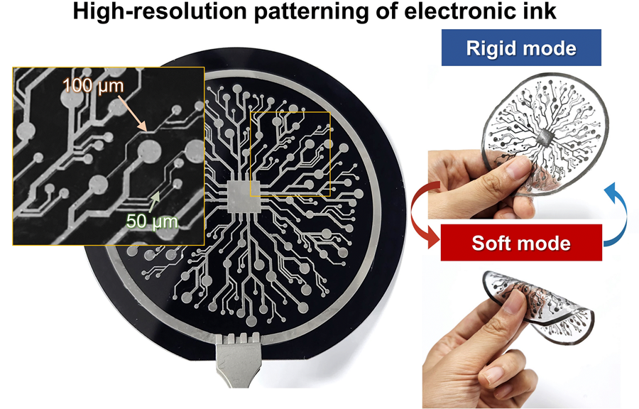
< Figure 1. Fabrication process of stable, high-viscosity electronic ink by dispersing micro-sized gallium particles in a polymer matrix (left). High-resolution large-area circuit printing process through pH-controlled chemical sintering (right). >
To address this challenge, the researchers focused on gallium, which melts just below body temperature. Solid gallium is quite stiff, while its liquid form is fluid and soft. Despite its potential, gallium’s use in electronic printing has been limited by its high surface tension and instability when melted.
To overcome these issues, the team developed a pH-controlled liquid metal ink printing process. By dispersing micro-sized gallium particles into a hydrophilic polyurethane matrix using a neutral solvent (dimethyl sulfoxide, or DMSO), they created a stable, high-viscosity ink suitable for precision printing. During post-print heating, the DMSO decomposes to form an acidic environment, which removes the oxide layer on the gallium particles. This triggers the particles to coalesce into electrically conductive networks with tunable mechanical properties.
The resulting printed circuits exhibit fine feature sizes (~50 μm), high conductivity (2.27 × 10⁶ S/m), and a stiffness modulation ratio of up to 1,465 – allowing the material to shift from plastic-like rigidity to rubber-like softness. Furthermore, the ink is compatible with conventional printing techniques such as screen printing and dip coating, supporting large-area and 3D device fabrication.
< Figure 2. Key features of the electronic ink. (i) High-resolution printing and multilayer integration capability. (ii) Batch fabrication capability through large-area screen printing. (iii) Complex three-dimensional structure printing capability through dip coating. (iv) Excellent electrical conductivity and stiffness control capability.>
The team demonstrated this technology by developing a multi-functional device that operates as a rigid portable electronic under normal conditions but transforms into a soft wearable healthcare device when attached to the body. They also created a neural probe that remains stiff during surgical insertion for accurate positioning but softens once inside brain tissue to reduce inflammation – highlighting its potential for biomedical implants.
< Figure 3. Variable stiffness wearable electronics with high-resolution circuits and multilayer structure comparable to commercial printed circuit boards (PCBs). Functions as a rigid portable electronic device at room temperature, then transforms into a wearable healthcare device by softening at body temperature upon skin contact.>
“The core achievement of this research lies in overcoming the longstanding challenges of liquid metal printing through our innovative technology,” said Professor Jeong. “By controlling the ink’s acidity, we were able to electrically and mechanically connect printed gallium particles, enabling the room-temperature fabrication of high-resolution, large-area circuits with tunable stiffness. This opens up new possibilities for future personal electronics, medical devices, and robotics.”
< Figure 4. Body-temperature softening neural probe implemented by coating electronic ink on an optical waveguide structure. (Left) Remains rigid during surgery for precise manipulation and brain insertion, then softens after implantation to minimize mechanical stress on the brain and greatly enhance biocompatibility. (Right) >
This research was published in Science Advances under the title, “Phase-Change Metal Ink with pH-Controlled Chemical Sintering for Versatile and Scalable Fabrication of Variable Stiffness Electronics.” The work was supported by the National Research Foundation of Korea, the Boston-Korea Project, and the BK21 FOUR Program.
2025.06.04 View 10446
KAIST Research Team Develops Electronic Ink for Room-Temperature Printing of High-Resolution, Variable-Stiffness Electronics
A team of researchers from KAIST and Seoul National University has developed a groundbreaking electronic ink that enables room-temperature printing of variable-stiffness circuits capable of switching between rigid and soft modes. This advancement marks a significant leap toward next-generation wearable, implantable, and robotic devices.
< Photo 1. (From left) Professor Jae-Woong Jeong and PhD candidate Simok Lee of the School of Electrical Engineering, (in separate bubbles, from left) Professor Gun-Hee Lee of Pusan National University, Professor Seongjun Park of Seoul National University, Professor Steve Park of the Department of Materials Science and Engineering>
Variable-stiffness electronics are at the forefront of adaptive technology, offering the ability for a single device to transition between rigid and soft modes depending on its use case. Gallium, a metal known for its high rigidity contrast between solid and liquid states, is a promising candidate for such applications. However, its use has been hindered by challenges including high surface tension, low viscosity, and undesirable phase transitions during manufacturing.
On June 4th, a research team led by Professor Jae-Woong Jeong from the School of Electrical Engineering at KAIST, Professor Seongjun Park from the Digital Healthcare Major at Seoul National University, and Professor Steve Park from the Department of Materials Science and Engineering at KAIST introduced a novel liquid metal electronic ink. This ink allows for micro-scale circuit printing – thinner than a human hair – at room temperature, with the ability to reversibly switch between rigid and soft modes depending on temperature.
The new ink combines printable viscosity with excellent electrical conductivity, enabling the creation of complex, high-resolution multilayer circuits comparable to commercial printed circuit boards (PCBs). These circuits can dynamically change stiffness in response to temperature, presenting new opportunities for multifunctional electronics, medical technologies, and robotics.
Conventional electronics typically have fixed form factors – either rigid for durability or soft for wearability. Rigid devices like smartphones and laptops offer robust performance but are uncomfortable when worn, while soft electronics are more comfortable but lack precise handling. As demand grows for devices that can adapt their stiffness to context, variable-stiffness electronics are becoming increasingly important.
< Figure 1. Fabrication process of stable, high-viscosity electronic ink by dispersing micro-sized gallium particles in a polymer matrix (left). High-resolution large-area circuit printing process through pH-controlled chemical sintering (right). >
To address this challenge, the researchers focused on gallium, which melts just below body temperature. Solid gallium is quite stiff, while its liquid form is fluid and soft. Despite its potential, gallium’s use in electronic printing has been limited by its high surface tension and instability when melted.
To overcome these issues, the team developed a pH-controlled liquid metal ink printing process. By dispersing micro-sized gallium particles into a hydrophilic polyurethane matrix using a neutral solvent (dimethyl sulfoxide, or DMSO), they created a stable, high-viscosity ink suitable for precision printing. During post-print heating, the DMSO decomposes to form an acidic environment, which removes the oxide layer on the gallium particles. This triggers the particles to coalesce into electrically conductive networks with tunable mechanical properties.
The resulting printed circuits exhibit fine feature sizes (~50 μm), high conductivity (2.27 × 10⁶ S/m), and a stiffness modulation ratio of up to 1,465 – allowing the material to shift from plastic-like rigidity to rubber-like softness. Furthermore, the ink is compatible with conventional printing techniques such as screen printing and dip coating, supporting large-area and 3D device fabrication.
< Figure 2. Key features of the electronic ink. (i) High-resolution printing and multilayer integration capability. (ii) Batch fabrication capability through large-area screen printing. (iii) Complex three-dimensional structure printing capability through dip coating. (iv) Excellent electrical conductivity and stiffness control capability.>
The team demonstrated this technology by developing a multi-functional device that operates as a rigid portable electronic under normal conditions but transforms into a soft wearable healthcare device when attached to the body. They also created a neural probe that remains stiff during surgical insertion for accurate positioning but softens once inside brain tissue to reduce inflammation – highlighting its potential for biomedical implants.
< Figure 3. Variable stiffness wearable electronics with high-resolution circuits and multilayer structure comparable to commercial printed circuit boards (PCBs). Functions as a rigid portable electronic device at room temperature, then transforms into a wearable healthcare device by softening at body temperature upon skin contact.>
“The core achievement of this research lies in overcoming the longstanding challenges of liquid metal printing through our innovative technology,” said Professor Jeong. “By controlling the ink’s acidity, we were able to electrically and mechanically connect printed gallium particles, enabling the room-temperature fabrication of high-resolution, large-area circuits with tunable stiffness. This opens up new possibilities for future personal electronics, medical devices, and robotics.”
< Figure 4. Body-temperature softening neural probe implemented by coating electronic ink on an optical waveguide structure. (Left) Remains rigid during surgery for precise manipulation and brain insertion, then softens after implantation to minimize mechanical stress on the brain and greatly enhance biocompatibility. (Right) >
This research was published in Science Advances under the title, “Phase-Change Metal Ink with pH-Controlled Chemical Sintering for Versatile and Scalable Fabrication of Variable Stiffness Electronics.” The work was supported by the National Research Foundation of Korea, the Boston-Korea Project, and the BK21 FOUR Program.
2025.06.04 View 10446 -
 KAIST perfectly reproduces Joseon-era Irworobongdo without pigments
Typically, chemical pigments that absorb specific wavelengths of light within the visible spectrum are required to produce colors. However, KAIST researchers have successfully reproduced the Joseon-era Irworobongdo [일월오봉도] painting using ultra-precise color graphics without any chemical pigments, allowing for the permanent and eco-friendly preservation of color graphics without fading or discoloration.
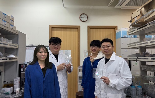
< (From left) Chaerim Son, a graduate of the Department of Biochemical Engineering (lead author), Seong Kyeong Nam, a graduate of the PhD program, Jiwoo Lee, a PhD student, and Professor Shin-Hyun Kim >
KAIST (represented by President Kwang Hyung Lee) announced on the 26th of February that a research team led by Professor Shinhyun Kim from the Department of Biological and Chemical Engineering had developed a technology that enables high-resolution color graphics without using any chemical pigments by employing hemisphere-shaped microstructures.
Morpho butterflies that are brilliant blue in color or Panther chameleons that change skin color exhibit coloration without chemical pigments, as ordered nanostructures within a material reflect visible light through optical interference. Since structural colors arise from physical structures rather than chemical substances, a single material can produce a wide range of colors.
However, the artificial implementation of structural coloration is highly challenging due to the complexity of creating ordered nanostructures. Additionally, it is difficult to produce a variety of colors and to pattern them precisely into complex designs.
< Figure 1. Principle of structural color expression using micro-hemispheres (left) and method of forming micro-hemisphere patterns based on photolithography (right) >
Professor Kim’s team overcame these challenges by using smooth-surfaced hemispherical microstructures instead of ordered nanostructures, enabling the high-precision patterning of diverse structural colors.
When light enters the inverted hemispherical microstructures, the portion of light entering from the sides undergoes total internal reflection along the curved surface, creating retroreflection. When the hemisphere diameter is approximately 10 micrometers (about one-tenth the thickness of a human hair), light traveling along different reflection paths interferes within the visible spectrum, producing structural coloration.
< Figure 2. “Irworobongdo”, the Painting of the Sun, Moon, and the Five Peaks, reproduced in fingernail size without pigment using approximately 200,000 micro-hemispheres >
The structural color can be tuned by adjusting the size of the hemispheres. By arranging hemispheres of varying sizes, much like mixing paints on a palette, an infinite range of colors can be generated.
To precisely pattern microscale hemispheres of different sizes, the research team employed photolithography* using positive photoresists** commonly used in semiconductor processing. They first patterned photoresists into micropillar structures, then induced reflow*** by heating the material, forming hemispherical microstructures.
*Photolithography: A technique used in semiconductor fabrication to pattern microscale structures.
**Positive photoresist: A photosensitive polymer that dissolves more easily in a developer solution after exposure to ultraviolet light.
***Reflow: A process in which a polymer material softens and reshapes into a curved structure when heated.
This method enables the formation of hemisphere-shaped microstructures with the desired sizes and colors in a single-step fabrication process. It also allows for the reproduction of arbitrary color graphics using a single material without any pigments.
The ultra-precise color graphics created with this technique can exhibit color variations depending on the angle of incident light or the viewing perspective. The pattern appears colored from one direction while remaining transparent from the opposite side, exhibiting a Janus effect. These structural color graphics achieve resolution comparable to cutting-edge LED displays, allowing complex color images to be captured within a fingernail-sized area and projected onto large screens.
< Figure 3. “Irworobongdo” that displays different shades depending on the angle of light and viewing direction >
Professor Shinhyun Kim, who led the research, stated, “Our newly developed pigment-free color graphics technology can serve as an innovative method for artistic expression, merging art with advanced materials. Additionally, it holds broad application potential in optical devices and sensors, anti-counterfeiting materials, aesthetic photocard printing, and many other fields.”
This research, with KAIST researcher Chaerim Son as the first author, was published in the prestigious materials science journal Advanced Materials on February 5.
(Paper title: “Retroreflective Multichrome Microdome Arrays Created by Single-Step Reflow”, DOI: 10.1002/adma.202413143 )
< Figure 4. Famous paintings reproduced without pigment: “Impression, Sunrise” (left), “Girl with a Pearl Earring” (right) >
The study was supported by the National Research Foundation of Korea through the Pioneer Converging Technology R&D Program and the Mid-Career Researcher Program.
2025.02.26 View 10480
KAIST perfectly reproduces Joseon-era Irworobongdo without pigments
Typically, chemical pigments that absorb specific wavelengths of light within the visible spectrum are required to produce colors. However, KAIST researchers have successfully reproduced the Joseon-era Irworobongdo [일월오봉도] painting using ultra-precise color graphics without any chemical pigments, allowing for the permanent and eco-friendly preservation of color graphics without fading or discoloration.
< (From left) Chaerim Son, a graduate of the Department of Biochemical Engineering (lead author), Seong Kyeong Nam, a graduate of the PhD program, Jiwoo Lee, a PhD student, and Professor Shin-Hyun Kim >
KAIST (represented by President Kwang Hyung Lee) announced on the 26th of February that a research team led by Professor Shinhyun Kim from the Department of Biological and Chemical Engineering had developed a technology that enables high-resolution color graphics without using any chemical pigments by employing hemisphere-shaped microstructures.
Morpho butterflies that are brilliant blue in color or Panther chameleons that change skin color exhibit coloration without chemical pigments, as ordered nanostructures within a material reflect visible light through optical interference. Since structural colors arise from physical structures rather than chemical substances, a single material can produce a wide range of colors.
However, the artificial implementation of structural coloration is highly challenging due to the complexity of creating ordered nanostructures. Additionally, it is difficult to produce a variety of colors and to pattern them precisely into complex designs.
< Figure 1. Principle of structural color expression using micro-hemispheres (left) and method of forming micro-hemisphere patterns based on photolithography (right) >
Professor Kim’s team overcame these challenges by using smooth-surfaced hemispherical microstructures instead of ordered nanostructures, enabling the high-precision patterning of diverse structural colors.
When light enters the inverted hemispherical microstructures, the portion of light entering from the sides undergoes total internal reflection along the curved surface, creating retroreflection. When the hemisphere diameter is approximately 10 micrometers (about one-tenth the thickness of a human hair), light traveling along different reflection paths interferes within the visible spectrum, producing structural coloration.
< Figure 2. “Irworobongdo”, the Painting of the Sun, Moon, and the Five Peaks, reproduced in fingernail size without pigment using approximately 200,000 micro-hemispheres >
The structural color can be tuned by adjusting the size of the hemispheres. By arranging hemispheres of varying sizes, much like mixing paints on a palette, an infinite range of colors can be generated.
To precisely pattern microscale hemispheres of different sizes, the research team employed photolithography* using positive photoresists** commonly used in semiconductor processing. They first patterned photoresists into micropillar structures, then induced reflow*** by heating the material, forming hemispherical microstructures.
*Photolithography: A technique used in semiconductor fabrication to pattern microscale structures.
**Positive photoresist: A photosensitive polymer that dissolves more easily in a developer solution after exposure to ultraviolet light.
***Reflow: A process in which a polymer material softens and reshapes into a curved structure when heated.
This method enables the formation of hemisphere-shaped microstructures with the desired sizes and colors in a single-step fabrication process. It also allows for the reproduction of arbitrary color graphics using a single material without any pigments.
The ultra-precise color graphics created with this technique can exhibit color variations depending on the angle of incident light or the viewing perspective. The pattern appears colored from one direction while remaining transparent from the opposite side, exhibiting a Janus effect. These structural color graphics achieve resolution comparable to cutting-edge LED displays, allowing complex color images to be captured within a fingernail-sized area and projected onto large screens.
< Figure 3. “Irworobongdo” that displays different shades depending on the angle of light and viewing direction >
Professor Shinhyun Kim, who led the research, stated, “Our newly developed pigment-free color graphics technology can serve as an innovative method for artistic expression, merging art with advanced materials. Additionally, it holds broad application potential in optical devices and sensors, anti-counterfeiting materials, aesthetic photocard printing, and many other fields.”
This research, with KAIST researcher Chaerim Son as the first author, was published in the prestigious materials science journal Advanced Materials on February 5.
(Paper title: “Retroreflective Multichrome Microdome Arrays Created by Single-Step Reflow”, DOI: 10.1002/adma.202413143 )
< Figure 4. Famous paintings reproduced without pigment: “Impression, Sunrise” (left), “Girl with a Pearl Earring” (right) >
The study was supported by the National Research Foundation of Korea through the Pioneer Converging Technology R&D Program and the Mid-Career Researcher Program.
2025.02.26 View 10480 -
 KAIST Research Team Develops an AI Framework Capable of Overcoming the Strength-Ductility Dilemma in Additive-manufactured Titanium Alloys
<(From Left) Ph.D. Student Jaejung Park and Professor Seungchul Lee of KAIST Department of Mechanical Engineering and , Professor Hyoung Seop Kim of POSTECH, and M.S.–Ph.D. Integrated Program Student Jeong Ah Lee of POSTECH. >
The KAIST research team led by Professor Seungchul Lee from Department of Mechanical Engineering, in collaboration with Professor Hyoung Seop Kim’s team at POSTECH, successfully overcame the strength–ductility dilemma of Ti 6Al 4V alloy using artificial intelligence, enabling the production of high strength, high ductility metal products. The AI developed by the team accurately predicts mechanical properties based on various 3D printing process parameters while also providing uncertainty information, and it uses both to recommend process parameters that hold high promise for 3D printing.
Among various 3D printing technologies, laser powder bed fusion is an innovative method for manufacturing Ti-6Al-4V alloy, renowned for its high strength and bio-compatibility. However, this alloy made via 3D printing has traditionally faced challenges in simultaneously achieving high strength and high ductility. Although there have been attempts to address this issue by adjusting both the printing process parameters and heat treatment conditions, the vast number of possible combinations made it difficult to explore them all through experiments and simulations alone.
The active learning framework developed by the team quickly explores a wide range of 3D printing process parameters and heat treatment conditions to recommend those expected to improve both strength and ductility of the alloy. These recommendations are based on the AI model’s predictions of ultimate tensile strength and total elongation along with associated uncertainty information for each set of process parameters and heat treatment conditions. The recommended conditions are then validated by performing 3D printing and tensile tests to obtain the true mechanical property values. These new data are incorporated into further AI model training, and through iterative exploration, the optimal process parameters and heat treatment conditions for producing high-performance alloys were determined in only five iterations. With these optimized conditions, the 3D printed Ti-6Al-4V alloy achieved an ultimate tensile strength of 1190 MPa and a total elongation of 16.5%, successfully overcoming the strength–ductility dilemma.
Professor Seungchul Lee commented, “In this study, by optimizing the 3D printing process parameters and heat treatment conditions, we were able to develop a high-strength, high-ductility Ti-6Al-4V alloy with minimal experimentation trials. Compared to previous studies, we produced an alloy with a similar ultimate tensile strength but higher total elongation, as well as that with a similar elongation but greater ultimate tensile strength.” He added, “Furthermore, if our approach is applied not only to mechanical properties but also to other properties such as thermal conductivity and thermal expansion, we anticipate that it will enable efficient exploration of 3D printing process parameters and heat treatment conditions.”
This study was published in Nature Communications on January 22 (https://doi.org/10.1038/s41467-025-56267-1), and the research was supported by the National Research Foundation of Korea’s Nano & Material Technology Development Program and the Leading Research Center Program.
2025.02.21 View 13000
KAIST Research Team Develops an AI Framework Capable of Overcoming the Strength-Ductility Dilemma in Additive-manufactured Titanium Alloys
<(From Left) Ph.D. Student Jaejung Park and Professor Seungchul Lee of KAIST Department of Mechanical Engineering and , Professor Hyoung Seop Kim of POSTECH, and M.S.–Ph.D. Integrated Program Student Jeong Ah Lee of POSTECH. >
The KAIST research team led by Professor Seungchul Lee from Department of Mechanical Engineering, in collaboration with Professor Hyoung Seop Kim’s team at POSTECH, successfully overcame the strength–ductility dilemma of Ti 6Al 4V alloy using artificial intelligence, enabling the production of high strength, high ductility metal products. The AI developed by the team accurately predicts mechanical properties based on various 3D printing process parameters while also providing uncertainty information, and it uses both to recommend process parameters that hold high promise for 3D printing.
Among various 3D printing technologies, laser powder bed fusion is an innovative method for manufacturing Ti-6Al-4V alloy, renowned for its high strength and bio-compatibility. However, this alloy made via 3D printing has traditionally faced challenges in simultaneously achieving high strength and high ductility. Although there have been attempts to address this issue by adjusting both the printing process parameters and heat treatment conditions, the vast number of possible combinations made it difficult to explore them all through experiments and simulations alone.
The active learning framework developed by the team quickly explores a wide range of 3D printing process parameters and heat treatment conditions to recommend those expected to improve both strength and ductility of the alloy. These recommendations are based on the AI model’s predictions of ultimate tensile strength and total elongation along with associated uncertainty information for each set of process parameters and heat treatment conditions. The recommended conditions are then validated by performing 3D printing and tensile tests to obtain the true mechanical property values. These new data are incorporated into further AI model training, and through iterative exploration, the optimal process parameters and heat treatment conditions for producing high-performance alloys were determined in only five iterations. With these optimized conditions, the 3D printed Ti-6Al-4V alloy achieved an ultimate tensile strength of 1190 MPa and a total elongation of 16.5%, successfully overcoming the strength–ductility dilemma.
Professor Seungchul Lee commented, “In this study, by optimizing the 3D printing process parameters and heat treatment conditions, we were able to develop a high-strength, high-ductility Ti-6Al-4V alloy with minimal experimentation trials. Compared to previous studies, we produced an alloy with a similar ultimate tensile strength but higher total elongation, as well as that with a similar elongation but greater ultimate tensile strength.” He added, “Furthermore, if our approach is applied not only to mechanical properties but also to other properties such as thermal conductivity and thermal expansion, we anticipate that it will enable efficient exploration of 3D printing process parameters and heat treatment conditions.”
This study was published in Nature Communications on January 22 (https://doi.org/10.1038/s41467-025-56267-1), and the research was supported by the National Research Foundation of Korea’s Nano & Material Technology Development Program and the Leading Research Center Program.
2025.02.21 View 13000 -
 Professor Sang-Min Bae receives the 2015 IDEA Awards
Professor Sang-min Bae of the Industrial Design Department at KAIST garnered one silver and two bronze awards from the 2015 International Design Excellence Awards (IDEA). Along with iF Design Award and Red Dot Design Awards, the IDEA is regarded as one of the world’s most respected recognition in the field of design.
Trash to Bin (T2B), a silver winner in the category of Social Impact Design, is a trash bin made of 1.87 lb (0.85 kg) of discarded papers. Using one-hundred percent recycled paper pulp, each T2B costs under $5 for production. The bin can be fully waterproofed for at least six hours. While satisfying with the industry safety standards, this environmentally-friendly bin can be produced on a large scale using litter energy, but offering the exact same benefit of a general garbage can.
Roll-Di, one of the two bronze winners, is a direction indicator that tells which string of screen curtains should be pulled to make the curtain go up or down. As shown in the picture below, Roll-Di can be installed at the bottom of the string, and the “up and down” arrows show which side of the string needs to be pulled to achieve the desired position of the curtain. This simple, yet handy solution to the problem that people frequently make the mistake of pulling the wrong string provides users with greater convenience.
The other bronze winner is Printing Solar-cell, an organic cartridge module that prints solar-cells using a domestic, ink-jet printer. With Printing Solar-cell, users can design their own cell patterns and charge their electronics anywhere holding the printed solar-cell on a copy paper.
Professor Bae said, “I’ve always tried to design something that is useful for people in need. I consider the IDEA awards an encouragement to keep up with my work toward that goal.”
Trash to Bin
Roll-Di
Printing Solar-cell
2015.09.30 View 14388
Professor Sang-Min Bae receives the 2015 IDEA Awards
Professor Sang-min Bae of the Industrial Design Department at KAIST garnered one silver and two bronze awards from the 2015 International Design Excellence Awards (IDEA). Along with iF Design Award and Red Dot Design Awards, the IDEA is regarded as one of the world’s most respected recognition in the field of design.
Trash to Bin (T2B), a silver winner in the category of Social Impact Design, is a trash bin made of 1.87 lb (0.85 kg) of discarded papers. Using one-hundred percent recycled paper pulp, each T2B costs under $5 for production. The bin can be fully waterproofed for at least six hours. While satisfying with the industry safety standards, this environmentally-friendly bin can be produced on a large scale using litter energy, but offering the exact same benefit of a general garbage can.
Roll-Di, one of the two bronze winners, is a direction indicator that tells which string of screen curtains should be pulled to make the curtain go up or down. As shown in the picture below, Roll-Di can be installed at the bottom of the string, and the “up and down” arrows show which side of the string needs to be pulled to achieve the desired position of the curtain. This simple, yet handy solution to the problem that people frequently make the mistake of pulling the wrong string provides users with greater convenience.
The other bronze winner is Printing Solar-cell, an organic cartridge module that prints solar-cells using a domestic, ink-jet printer. With Printing Solar-cell, users can design their own cell patterns and charge their electronics anywhere holding the printed solar-cell on a copy paper.
Professor Bae said, “I’ve always tried to design something that is useful for people in need. I consider the IDEA awards an encouragement to keep up with my work toward that goal.”
Trash to Bin
Roll-Di
Printing Solar-cell
2015.09.30 View 14388 -
 Prof. Park to Receive HP's Annual Innovation Research Award
Prof. In-Kyu Park of the Department of Mechanical Engineering, KAIST, has been will receive an award from Hewlett-Packard"s second annual Labs Innovation Research Program, university authorities said on Wednesday (July 8).
Prof. Park was chosen as the winner of the research award for his paper entitled "Eco-friendly nanomanufacturing for intelligent environment sensing applications."
Sixty projects from 46 universities in 12 countries were selected as the recipients of the awards from HP Labs, the company"s central research arm. The program is designed to create opportunities for colleges, universities and research institutes to conduct collaborative research with HP.
HP Labs Innovation Research Awards provide project funding of up to $100,000 for one year to each of the chosen academic institutions, which is renewable for up to three years based on research progress and HP business requirements.
Prof. Park has conducted joint researches on nanoimprinting, nanosensors, and nanoelectronics with HP"s Information and Quantum Systems Lab since 2005. Starting from the later half of 2009, he is to receive research grants under the industry-academia cooperation program of the world"s information technology giant firm.
2009.07.09 View 22740
Prof. Park to Receive HP's Annual Innovation Research Award
Prof. In-Kyu Park of the Department of Mechanical Engineering, KAIST, has been will receive an award from Hewlett-Packard"s second annual Labs Innovation Research Program, university authorities said on Wednesday (July 8).
Prof. Park was chosen as the winner of the research award for his paper entitled "Eco-friendly nanomanufacturing for intelligent environment sensing applications."
Sixty projects from 46 universities in 12 countries were selected as the recipients of the awards from HP Labs, the company"s central research arm. The program is designed to create opportunities for colleges, universities and research institutes to conduct collaborative research with HP.
HP Labs Innovation Research Awards provide project funding of up to $100,000 for one year to each of the chosen academic institutions, which is renewable for up to three years based on research progress and HP business requirements.
Prof. Park has conducted joint researches on nanoimprinting, nanosensors, and nanoelectronics with HP"s Information and Quantum Systems Lab since 2005. Starting from the later half of 2009, he is to receive research grants under the industry-academia cooperation program of the world"s information technology giant firm.
2009.07.09 View 22740 -
 KAIST Opens CFTS
- To research the prevention of the illegal production of security technologies
- Total 1.5 billion won of research expenses and 102 researchers to be invested for the next three years- Opening ceremony at the computer science building, KAIST on April 13 at 10 am
KAIST (President Nam-Pyo Suh) will open ‘the Center of Fusion Technology for Security (CFTS)’ under the auspices of the Korea Minting & Security Printing Corporation (KOMSCO, President Hae-Sung Lee) to undertake researches over the prevention of illegal reproduction of security technologies. The opening ceremony was held at the computer science building, KAIST on Friday, April 13.
Total .1.5 billion won of research expenses and 102 researchers will be invested in the center for the next three years.
Main research fields are ▲ advanced IT-based information concealment methods ▲ utilization of energy transfer luminescence in host guest nano-substances ▲ the utilization of quantum-dot, non-crystal carbon and piezoelectric elements ▲ development of radio frequency identification (RFID), optical, biological security element-applied technologies, etc.
“We’ll develop fusion technologies for security that can easily detect forgeries and alterations of security products by introducing advanced IT, optical, chemical engineering, and biological elements. The development of core technologies applied to security products will activate domestic security markets and enable the export of relevant technologies,” said General Research Director Heung-Kyu Lee, a professor of Computer Sciences.
2007.04.19 View 20748
KAIST Opens CFTS
- To research the prevention of the illegal production of security technologies
- Total 1.5 billion won of research expenses and 102 researchers to be invested for the next three years- Opening ceremony at the computer science building, KAIST on April 13 at 10 am
KAIST (President Nam-Pyo Suh) will open ‘the Center of Fusion Technology for Security (CFTS)’ under the auspices of the Korea Minting & Security Printing Corporation (KOMSCO, President Hae-Sung Lee) to undertake researches over the prevention of illegal reproduction of security technologies. The opening ceremony was held at the computer science building, KAIST on Friday, April 13.
Total .1.5 billion won of research expenses and 102 researchers will be invested in the center for the next three years.
Main research fields are ▲ advanced IT-based information concealment methods ▲ utilization of energy transfer luminescence in host guest nano-substances ▲ the utilization of quantum-dot, non-crystal carbon and piezoelectric elements ▲ development of radio frequency identification (RFID), optical, biological security element-applied technologies, etc.
“We’ll develop fusion technologies for security that can easily detect forgeries and alterations of security products by introducing advanced IT, optical, chemical engineering, and biological elements. The development of core technologies applied to security products will activate domestic security markets and enable the export of relevant technologies,” said General Research Director Heung-Kyu Lee, a professor of Computer Sciences.
2007.04.19 View 20748