ANS
-
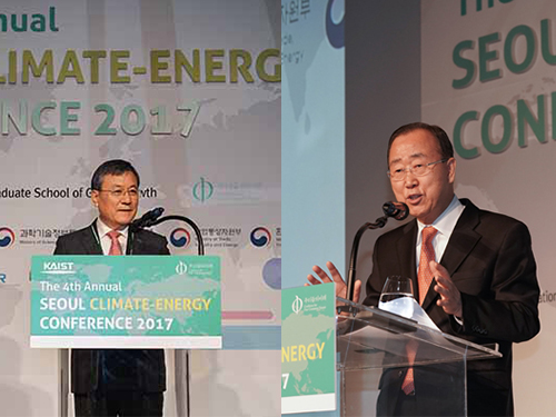 Seoul Climate-Energy Conference Seeks Global Sustainability
(President Shin and Former UN Secretary General at the Seoul Climate Change-Energy Conference)
Global leaders from both the private and public sectors discussed creative ways to seek inclusive green growth and sustainable development at the Seoul Climate-Energy Conference on November 24 in Seoul. The annual conference was co-hosted by KAIST and the Coalition for Our Common Future under the theme “Creating New Momentum for the Paris Agreement and a Sustainable Future.”
More than 100 global leaders participated in the forum including the Director General Frank Rijsbermanof the Global Green Growth Institute and Executive Director Howard Bamsey of the Green Climate Fund. Former UN Secretary-General Ban Ki-Moon, who played a significant role in the signing of the Paris Agreement, was the keynote speaker.
This year’s conference focused on Korea’s low carbon-energy transition and the Fourth Industrial Revolution to be aligned with green growth. At the conference, speakers and participants reviewed the progress of the decisions made by the UN Framework Convention on Climate Change (UNFCCC) COP23 in Bonn, Germany. The conference discussed topics of global collaboration for new climate regimes, green energy infrastructure, the Asia super grid, financing green energy, smart green cities, and new mobility.
President Sung-Chul Shin emphasized global action and greater resilience toward climate change in his opening remarks. He said, “Today’s climate change can be attributed directly to the past three industrial revolutions. As industrialization continues, we must not make future generations pay the cost of this Fourth Industrial Revolution.” He explained that it is increasingly complicated to address climate change and energy issues because even though the use of energy consumption will continue to increase, energy policies are interwoven with global politics.
He stressed three keywords to better address this global problem: innovation, collaboration, and speed. First he emphasized innovation as a priority for future success as it is hard to retain confidence without innovation.
He noted KAIST has made sustainability initiatives in the fields of EEWS (energy, environment, water, sustainability) and green mobility. He also noted the importance of collaboration as industries are moving beyond a single discipline. KAIST is making collaborations in R&D and sustainability sectors, such as Saudi Aramco’s CO2 management center in KAIST. Finally, he explained that the speed of new transformation will be beyond our imagination, and governments should work efficiently to address issues in a fast manner.
Meanwhile, Secretary-General Ban called for global unity in addressing climate change. He strongly emphasized that countries should make agreements not of willingness but of action, and that politicians should realize that this global agenda should be given top priority above domestic politics. He addressed how the world is experiencing the most powerful and destructive effects of climate change which makes active participation in the Paris Agreement increasingly important.
He expressed his concern that the richest and most powerful countries are backing off, emphasizing the role of these countries as both global leaders and top producers of CO2. He also shared his hopes that the OECD will continue to work to fill the absence of the United States, and stressed the importance of acquiring 10 billion USD by 2020 to fund mitigation and adaptation technologies for developing countries’ CO2 emissions.
Click for President Shin's opening remarks
2017.11.29 View 9841
 -
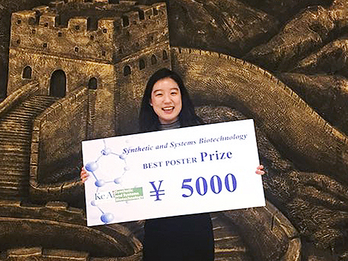 In Jin Cho Earned the Best Poster Prize at ME Summit 2017
In Jin Cho, a Ph.D. student in the Department of Chemical and Biomolecular Engineering at KAIST received the best poster prize at the International Metabolic Engineering Summit 2017 held on October 24 in Beijing, China.
The International Metabolic Engineering Summit is a global conference where scientists and corporate researchers in the field of metabolic engineering present their latest research outcomes and build networks.
At this year’s summit, about 500 researchers from around the world participated in active academic exchanges, including giving keynote speeches and presenting posters.
During the poster session, the summit selects one person for the KeAi-synthetic and Systems Biotechnology Poster Award, two for Microbial Cell Factories Poster Awards, and three for Biotechnology Journal Poster Awards among the posters presented by graduate students, post-doctoral fellows and researchers. Cho received the KeAi-synthetic and Systems Biotechnology Poster Award. Her winning poster is on the biotransformation of p-xylene to terephthalic acid using engineered Escherichia coli.
Terephthalic acid is generally produced by p-xylene oxidation; however, this process requires a high temperature and pressure as well as a toxic catalyst during the reaction process.
Cho and Ziwei Luo, a Ph.D. student at KAIST, co-conducted the research and developed a successful biological conversion process. Compared to the existing chemical process, it does not require a high temperature and pressure; and it is environmentally friendly with a relatively high conversion rate of approximately 97%.
Cho’s advisor, Distinguished Professor Sang Yup Lee said, “Further research on glucose-derived terephthalic acid will enable us to produce biomass-based eco-friendly terephthalic acid through engineered Escherichia coli.”
2017.10.31 View 11549
 -
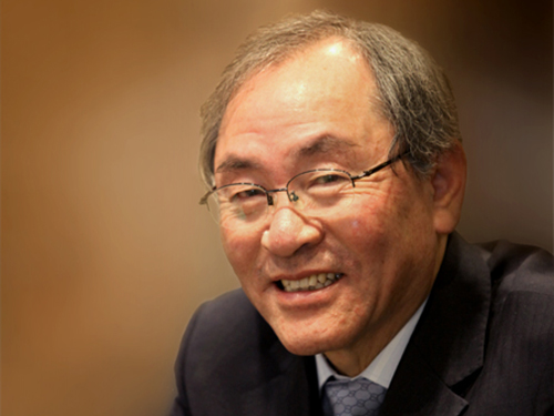 Professor Nam Jin Cho Selected as the Eugene P. Wigner Reactor Physicist Awardee
Professor Nam Jin Cho from the Department of Nuclear & Quantum Engineering was selected as the recipient of the 2017 ‘Eugene P. Wigner Reactor Physicist Award.’ The award, established in 1990 by the American Nuclear Society, honors individuals who have made outstanding contributions to the advancement of the field of reactor physics. The award is named after the late Eugene P. Wigner, a pioneer who helped nurture the nuclear age to technical maturity with his pioneering leadership in reactor design.
Professor Cho was recognized for his outstanding leadership and achievement in the field of nuclear physics, especially with his original research in analytic function expansion nodal methods, coarse-mesh angular dependent rebalance methods, and neutron transport calculations. A fellow of the ANS, Professor Cho is the first awardee from the Asian region.
Professor Cho gave all the credit to his colleagues and students at KAIST who have spared no effort while working together for three decades. “I am very grateful for the unique academic ambience which made this challenging work possible as well as the government’s continuing funding at the National Research Laboratory project.
2017.07.12 View 8554
 -
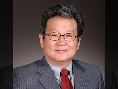 Professor Poong Hyun Seong Selected as Fellow of the ANS
Professor Poong Hyun Seong of the Department of Nuclear and Quantum Engineering was selected as a fellow of the American Nuclear Society.
The selection was announced at their annual meeting held in San Francisco on June 12, in recognition of Professor Seong's contributions to the field of nuclear instrumentation, control andhuman factors engineering.
Founded in 1954, the American Nuclear Society selects scholars who have made outstanding achievements and contributions to the development of the nuclear engineering field each year.
Professor Seong's researches in the field of nuclear instrumentation, control and human factors engineering have contributed to the safe operation of nuclear power plants, to the development of systems to maintain nuclear power plants safely in the event of emergency and to the enhancement of effective response capabilities of nuclear power plant operators. His researches significantly contributed to the safety improvement of nuclear power plants and have been recognized worldwide.
Professor Seong said, "Korea has emerged as a nuclear powerhouse. I think not only my academic career but our national reputation in the field of nuclear research has been well recognized by our global peers.” Professor Seong has served as president of the Korean Nuclear Society, editor in chief of Nuclear Engineering and Technology, and as a commissioner of the Korean Nuclear Safety Commission. He is currently working as a commissioner of the Korean Atomic Energy Commission.
2017.06.29 View 9015
 -
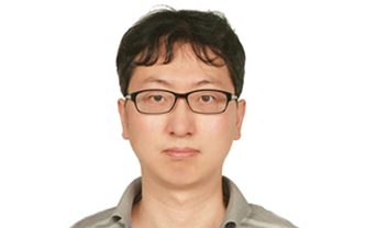 Professor Lee Recognized by the KMS as Best Paper Awardee
Professor Ji Oon Lee of the Department of Mathematical Sciences was selected as the 2017 Best Paper Awardee by the Korean Mathematical Society. The award will be presented during the KMS spring meeting on April 29. Dr. Lee is being honored for proving a necessary and sufficient condition for the Tracy-Wisdom law of Wigner matrices. In a paper titled ‘A Necessary and Sufficient Condition for Edge Universality of Wigner Matrices,’ he proposed a solution for one of the many unanswered problems in the field of random matrix theory that have existed for decades. The paper, co-authored with Professor Jun Yin at the University of Wisconsin – Madison, was published in the Duke Mathematical Journal in 2014. Professor Lee joined KAIST in 2010 after finishing his Ph.D. at Harvard University. He was named a ‘POSCI Science Fellow’ and received the ‘Young Scientist Award’ from the KMS in 2014.
2017.04.27 View 10900
 -
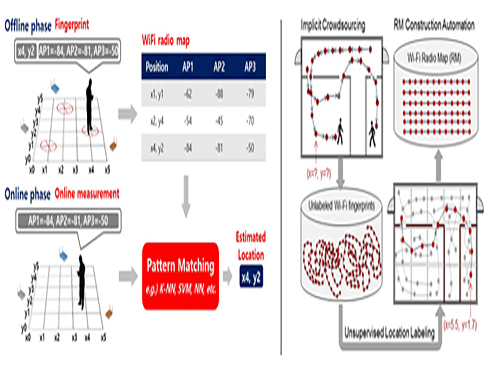 Crowdsourcing-Based Global Indoor Positioning System
Research team of Professor Dong-Soo Han of the School of Computing Intelligent Service Lab at KAIST developed a system for providing global indoor localization using Wi-Fi signals. The technology uses numerous smartphones to collect fingerprints of location data and label them automatically, significantly reducing the cost of constructing an indoor localization system while maintaining high accuracy.
The method can be used in any building in the world, provided the floor plan is available and there are Wi-Fi fingerprints to collect. To accurately collect and label the location information of the Wi-Fi fingerprints, the research team analyzed indoor space utilization. This led to technology that classified indoor spaces into places used for stationary tasks (resting spaces) and spaces used to reach said places (transient spaces), and utilized separate algorithms to optimally and automatically collect location labelling data.
Years ago, the team implemented a way to automatically label resting space locations from signals collected in various contexts such as homes, shops, and offices via the users’ home or office address information. The latest method allows for the automatic labelling of transient space locations such as hallways, lobbies, and stairs using unsupervised learning, without any additional location information. Testing in KAIST’s N5 building and the 7th floor of N1 building manifested the technology is capable of accuracy up to three or four meters given enough training data. The accuracy level is comparable to technology using manually-labeled location information.
Google, Microsoft, and other multinational corporations collected tens of thousands of floor plans for their indoor localization projects. Indoor radio map construction was also attempted by the firms but proved more difficult. As a result, existing indoor localization services were often plagued by inaccuracies. In Korea, COEX, Lotte World Tower, and other landmarks provide comparatively accurate indoor localization, but most buildings suffer from the lack of radio maps, preventing indoor localization services.
Professor Han said, “This technology allows the easy deployment of highly accurate indoor localization systems in any building in the world. In the near future, most indoor spaces will be able to provide localization services, just like outdoor spaces.” He further added that smartphone-collected Wi-Fi fingerprints have been unutilized and often discarded, but now they should be treated as invaluable resources, which create a new big data field of Wi-Fi fingerprints. This new indoor navigation technology is likely to be valuable to Google, Apple, or other global firms providing indoor positioning services globally. The technology will also be valuable for helping domestic firms provide positioning services.
Professor Han added that “the new global indoor localization system deployment technology will be added to KAILOS, KAIST’s indoor localization system.” KAILOS was released in 2014 as KAIST’s open platform for indoor localization service, allowing anyone in the world to add floor plans to KAILOS, and collect the building’s Wi-Fi fingerprints for a universal indoor localization service. As localization accuracy improves in indoor environments, despite the absence of GPS signals, applications such as location-based SNS, location-based IoT, and location-based O2O are expected to take off, leading to various improvements in convenience and safety. Integrated indoor-outdoor navigation services are also visible on the horizon, fusing vehicular navigation technology with indoor navigation.
Professor Han’s research was published in IEEE Transactions on Mobile Computing (TMC) in November in 2016.
For more, please visit http://ieeexplore.ieee.org/stamp/stamp.jsp?arnumber=7349230http://ieeexplore.ieee.org/document/7805133/
2017.04.06 View 10633
 -
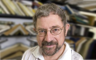 Nobel Laureate Dr. John Michael Kosterlitz Speaks at KAIST
KAIST’s Department of Physics will invite one of three co-recipients of the Nobel Prize in Physics 2016, Professor John Michael Kosterlitz of Brown University, on January 9, 2017, to speak about the exotic states of matter, which is entitled “Topological Defects and Phase Transitions.”
Professor Kosterlitz shares the Nobel award with two other researchers, David Thouless and Duncan Haldane. He is considered one of the pioneers in the field of topological phases. In the early 1970s, along with Thouless, he demonstrated that superconductivity could occur at low temperatures and explained the mechanism behind, phase transition, that makes superconductivity disappear at higher temperatures.
Over the last decade, topological materials and their applications have been widely studied with the hope of using them in new generations of electronics and superconductors, or in future quantum computers. Details of the lecture follow below:
Distinguished Lecture Series by KAIST’s Physics Department
· Speaker: Professor John Michael Kosterlitz of the Physics Department,
Brown University
· Topic: “Topological Defects and Phase Transitions”
· Date: January 9, 2017, 4:00 PM
· Place: Lecture Hall (#1501), College of Natural Sciences (E6-2)
2017.01.06 View 8631
 -
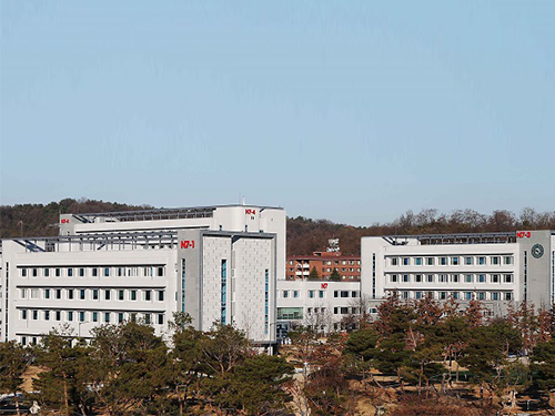 Mechanical Engineering Building on Campus Refurbished
KAIST’s Mechanical Engineering Department has finished the project to remodel its buildings and hosted an opening ceremony on December 12, 2016, which was attended by the university’s senior management and guests including President Steve Kang and Choong-Hwan Ahn, Architecture Policy Officer at the Ministry of Land, Infrastructure and Transport of Korea (MLIT).
With an investment of approximately USD 10 million, the old buildings (each consisting of seven floors and one basement) were transformed into smart, green buildings. Among the upgrades were the establishment of LED lighting systems, the replacement of the exterior walls with insulated materials, and the installation of double-glazed windows, all resulting in the improvement of the buildings’ energy efficiency. Previously, offices and lecture halls in the buildings had individual cooling and heating systems, which consumed a great deal of energy, but they were replaced with a centralized smart energy control system that monitors the operation status as well as energy consumption in real time.
With these new improvements, the Department was able to slash its energy consumption by 32%, for which it received Green Building Conversion Certification from MLIT. The ministry issues the certification to buildings that reduce their energy consumption by over 20% as a result of infrastructure upgrades. Beginning with the Mechanical Engineering buildings, KAIST will work on obtaining this certification for all of its buildings that are either under renovation or construction.
President Kang said, “We are pleased to offer our students a comfortable environment for study and research and will continue improving outdated facilities and infrastructure to make the campus safer and nicer.”
Picture 1: Ribbon-cutting ceremony for the refurbished Mechanical Engineering buildings on campus
Picture 2: Mechanical engineering buildings
2016.12.09 View 8327
 -
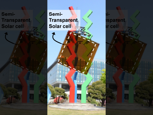 KAIST Team Develops Semi-Transparent Solar Cells with Thermal Mirror Capability
A research team led by KAIST and Sungkyunkwan University professors has created semi-transparent perovskite solar cells that demonstrate high-power conversion efficiency and transmit visible light while blocking infrared light, making them great candidates for solar windows.
Modern architects prefer to build exteriors designed with glass mainly from artistic or cost perspectives. Scientists, however, go one step further and see opportunities from its potential ability to harness solar energy. Researchers have thus explored ways to make solar cells transparent or semi-transparent as a substitute material for glass, but this has proven to be a challenging task because solar cells need to absorb sunlight to generate electricity, and when they are transparent, it reduces their energy efficiency.
Typical solar cells today are made of crystalline silicon, but it is difficult to make them translucent. Semi-transparent solar cells under development use, for example, organic or dye-sensitized materials, but compared to crystalline silicon-based cells, their power-conversion efficiencies are relatively low. Perovskites are hybrid organic-inorganic halide-based photovoltaic materials, which are cheap to produce and easy to manufacture. They have recently received much attention as the efficiency of perovskite solar cells has rapidly increased to the level of silicon technologies in the past few years.
Using perovskites, a Korean research team led by Professor Seunghyup Yoo of the Electrical Engineering School at KAIST and Professor Nam-Gyu Park of the Chemical Engineering School at Sungkyunkwan University developed a semi-transparent solar cell that is highly efficient and, additionally, functions very effectively as a thermal-mirror.
The team has developed a top transparent electrode (TTE) that works well with perovskite solar cells. In most cases, a key to success in realizing semi-transparent solar cells is to find a TTE that is compatible with a given photoactive material system, which is also the case for perovskite solar cells. The proposed TTE is based on a multilayer stack consisting of a metal film sandwiched between a high refractive-index (high-index) layer and an interfacial buffer layer. This TTE, placed as a top-most layer, can be prepared without damaging ingredients used in perovskite solar cells. Unlike conventional transparent electrodes focusing only on transmitting visible light, the proposed TTE plays the dual role of passing through visible light while reflecting infrared rays. The semi-transparent solar cells made with the proposed TTEs exhibited average power conversion efficiency as high as 13.3% with 85.5% infrared rejection.
The team believes that if the semi-transparent perovskite solar cells are scaled up for practical applications, they can be used in solar windows for buildings and automobiles, which not only generate electrical energy but also enable the smart heat management for indoor environments, thereby utilizing solar energy more efficiently and effectively.
This result was published as a cover article in the July 20, 2016 issue of Advanced Energy Materials. The research paper is entitled “Empowering Semi-transparent Solar Cells with Thermal-mirror Functionality.” (DOI: 10.1002/aenm.201502466)
The team designed the transparent electrode (TE) stack in three layers: A thin-film of silver (Ag) is placed in between the bottom interfacial layer of molybdenum trioxide (MoO3) and the top high-index dielectric layer of zinc sulfide (ZnS). Such a tri-layer approach has been known as a means to increase the overall visible-light transmittance of metallic thin films via index matching technique, which is essentially the same technique used for anti-reflection coating of glasses except that the present case involves a metallic layer.
Traditionally, when a TE is based on a metal film, such as Ag, the film should be extremely thin, e.g., 7-12 nanometers (nm), to obtain transparency and, accordingly, to transmit visible light. However, the team took a different approach in this research. They made the Ag TE two or three times thicker (12-24 nm) than conventional metal films and, as a result, it reflected more infrared light. The high refractive index of the ZnS layer plays an essential role in keeping the visible light transmittance of the proposed TTE high even with the relatively thick Ag film when its thickness is carefully optimized for maximal destructive interference, leading to low reflectance (and thus high transmittance) within its visible light range.
The team confirmed the semi-transparent perovskite solar cell’s thermal-mirror function through an experiment in which a halogen lamp illuminated an object for five minutes through three mediums: a window of bare glass, automotive tinting film, and the proposed semi-transparent perovskite solar cell. An infrared (IR) camera took thermal images of the object as well as that of each window’s surface. The object’s temperature, when exposed through the glass window, rose to 36.8 Celsius degrees whereas both the tinting film and the cell allowed the object to remain below 27 Celsius degrees. The tinting film absorbs light to block solar energy, so the film’s surface became hot as it was continuously exposed to the lamp light, but the proposed semi-transparent solar cell stayed cool since it rejects solar heat energy by reflection, rather than by absorption. The total solar energy rejection (TSER) of the proposed cell was as high as 89.6%.
Professor Yoo of KAIST said, “The major contributions of this work are to find transparent electrode technology suitable for translucent perovskite cells and to provide a design approach to fully harness the potential it can further deliver as a heat mirror in addition to its main role as an electrode. The present work can be further fine-tuned to include colored solar cells and to incorporate flexible or rollable form factors, as they will allow for greater design freedom and thus offer more opportunities for them to be integrated into real-world objects and structures such as cars, buildings, and houses.”
The lead authors are Hoyeon Kim and Jaewon Ha, both Ph.D. candidates in the School of Electrical Engineering at KAIST, and Hui-Seon Kim, a student in the School of Chemical Engineering at Sungkyunkwan University. This research was supported mainly by the Climate Change Research Hub Program of KAIST.
Picture 1: Semi-transparent Perovskite Solar Cell
This picture shows a prototype of a semi-transparent perovskite solar cell with thermal-mirror functionality.
Picture 2: A Heat Rejection Performance Comparison Experiment
This picture presents thermal images taken by an infrared camera for comparing the heat rejection performance of bare glass, automotive tinting film, and a semi-transparent perovskite solar cell after being illuminated by a halogen lamp for five minutes.
2016.08.02 View 13513
 -
 KAIST Develops Transparent Oxide Thin-Film Transistors
With the advent of the Internet of Things (IoT) era, strong demand has grown for wearable and transparent displays that can be applied to various fields such as augmented reality (AR) and skin-like thin flexible devices. However, previous flexible transparent displays have posed real challenges to overcome, which are, among others, poor transparency and low electrical performance. To improve the transparency and performance, past research efforts have tried to use inorganic-based electronics, but the fundamental thermal instabilities of plastic substrates have hampered the high temperature process, an essential step necessary for the fabrication of high performance electronic devices.
As a solution to this problem, a research team led by Professors Keon Jae Lee and Sang-Hee Ko Park of the Department of Materials Science and Engineering at the KAIST has developed ultrathin and transparent oxide thin-film transistors (TFT) for an active-matrix backplane of a flexible display by using the inorganic-based laser lift-off (ILLO) method. Professor Lee’s team previously demonstrated the ILLO technology for energy-harvesting (Advanced Materials, February 12, 2014) and flexible memory (Advanced Materials, September 8, 2014) devices.
The research team fabricated a high-performance oxide TFT array on top of a sacrificial laser-reactive substrate. After laser irradiation from the backside of the substrate, only the oxide TFT arrays were separated from the sacrificial substrate as a result of reaction between laser and laser-reactive layer, and then subsequently transferred onto ultrathin plastics ( thickness). Finally, the transferred ultrathin-oxide driving circuit for the flexible display was attached conformally to the surface of human skin to demonstrate the possibility of the wearable application. The attached oxide TFTs showed high optical transparency of 83% and mobility of even under several cycles of severe bending tests.
Professor Lee said, “By using our ILLO process, the technological barriers for high performance transparent flexible displays have been overcome at a relatively low cost by removing expensive polyimide substrates. Moreover, the high-quality oxide semiconductor can be easily transferred onto skin-like or any flexible substrate for wearable application.”
These research results, entitled “Skin-Like Oxide Thin-Film Transistors for Transparent Displays,”
(http://onlinelibrary.wiley.com/doi/10.1002/adfm.201601296/abstract) were the lead article published in the July 2016 online issue of Wiley’s Advanced Functional Materials.
###
References
[1] Advanced Materials, February 12, 2014, Highly-efficient, Flexible Piezoelectric PZT Thin Film Nanogenerator on Plastic Substrates
(http://onlinelibrary.wiley.com/doi/10.1002/adma.201305659/abstract)
[2] Advanced Materials, September 8, 2014, Flexible Crossbar-structured Resistive Memory Arrays on Plastic Substartes via Inorganic-based Laser Lift-off
(http://onlinelibrary.wiley.com/doi/10.1002/adma.201402472/abstract)
Picture 1: A Schamatic Image of Ultrathin, Flexible, and Transparent Oxide Thin-film Transistors
This image shows ultrathin, flexible, and transparent oxide thin-film transistors produced via the ILLO process.
Picture 2: Application of Uultrathin, Flexible, and Transparent Oxide Thin-film Transistors
This picture shows ultrathin, flexible, and transparent oxide thin-film transistors attached to a jumper sleeve and human skin.
2016.08.01 View 13376
 -
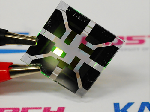 Graphene-Based Transparent Electrodes for Highly Efficient Flexible OLEDs
A Korean research team developed an ideal electrode structure composed of graphene and layers of titanium dioxide and conducting polymers, resulting in highly flexible and efficient OLEDs.
The arrival of a thin and lightweight computer that even rolls up like a piece of paper will not be in the far distant future. Flexible organic light-emitting diodes (OLEDs), built upon a plastic substrate, have received greater attention lately for their use in next-generation displays that can be bent or rolled while still operating.
A Korean research team led by Professor Seunghyup Yoo from the School of Electrical Engineering, KAIST and Professor Tae-Woo Lee from the Department of Materials Science and Engineering, Pohang University of Science and Technology (POSTECH) has developed highly flexible OLEDs with excellent efficiency by using graphene as a transparent electrode (TE) which is placed in between titanium dioxide (TiO2) and conducting polymer layers. The research results were published online on June 2, 2016 in Nature Communications.
OLEDs are stacked in several ultra-thin layers on glass, foil, or plastic substrates, in which multi-layers of organic compounds are sandwiched between two electrodes (cathode and anode). When voltage is applied across the electrodes, electrons from the cathode and holes (positive charges) from the anode draw toward each other and meet in the emissive layer. OLEDs emit light as an electron recombines with a positive hole, releasing energy in the form of a photon. One of the electrodes in OLEDs is usually transparent, and depending on which electrode is transparent, OLEDs can either emit from the top or bottom.
In conventional bottom-emission OLEDs, an anode is transparent in order for the emitted photons to exit the device through its substrate. Indium-tin-oxide (ITO) is commonly used as a transparent anode because of its high transparency, low sheet resistance, and well-established manufacturing process. However, ITO can potentially be expensive, and moreover, is brittle, being susceptible to bending-induced formation of cracks.
Graphene, a two-dimensional thin layer of carbon atoms tightly bonded together in a hexagonal honeycomb lattice, has recently emerged as an alternative to ITO. With outstanding electrical, physical, and chemical properties, its atomic thinness leading to a high degree of flexibility and transparency makes it an ideal candidate for TEs. Nonetheless, the efficiency of graphene-based OLEDs reported to date has been, at best, about the same level of ITO-based OLEDs.
As a solution, the Korean research team, which further includes Professors Sung-Yool Choi (Electrical Engineering) and Taek-Soo Kim (Mechanical Engineering) of KAIST and their students, proposed a new device architecture that can maximize the efficiency of graphene-based OLEDs. They fabricated a transparent anode in a composite structure in which a TiO2 layer with a high refractive index (high-n) and a hole-injection layer (HIL) of conducting polymers with a low refractive index (low-n) sandwich graphene electrodes. This is an optical design that induces a synergistic collaboration between the high-n and low-n layers to increase the effective reflectance of TEs. As a result, the enhancement of the optical cavity resonance is maximized. The optical cavity resonance is related to the improvement of efficiency and color gamut in OLEDs. At the same time, the loss from surface plasmon polariton (SPP), a major cause for weak photon emissions in OLEDs, is also reduced due to the presence of the low-n conducting polymers.
Under this approach, graphene-based OLEDs exhibit 40.8% of ultrahigh external quantum efficiency (EQE) and 160.3 lm/W of power efficiency, which is unprecedented in those using graphene as a TE. Furthermore, these devices remain intact and operate well even after 1,000 bending cycles at a radius of curvature as small as 2.3 mm. This is a remarkable result for OLEDs containing oxide layers such as TiO2 because oxides are typically brittle and prone to bending-induced fractures even at a relatively low strain. The research team discovered that TiO2 has a crack-deflection toughening mechanism that tends to prevent bending-induced cracks from being formed easily.
Professor Yoo said, “What’s unique and advanced about this technology, compared with previous graphene-based OLEDs, is the synergistic collaboration of high- and low-index layers that enables optical management of both resonance effect and SPP loss, leading to significant enhancement in efficiency, all with little compromise in flexibility.” He added, “Our work was the achievement of collaborative research, transcending the boundaries of different fields, through which we have often found meaningful breakthroughs.”
Professor Lee said, “We expect that our technology will pave the way to develop an OLED light source for highly flexible and wearable displays, or flexible sensors that can be attached to the human body for health monitoring, for instance.”
The research paper is entitled “Synergistic Electrode Architecture for Efficient Graphene-based Flexible Organic Light-emitting Diodes” (DOI. 10.1038/NCOMMS11791). The lead authors are Jae-Ho Lee, a Ph.D. candidate at KAIST; Tae-Hee Han, a Ph.D. researcher at POSTECH; and Min-Ho Park, a Ph.D. candidate at POSTECH.
This study was supported by the Basic Science Research Program of the National Research Foundation of Korea (NRF) through the Center for Advanced Flexible Display (CAFDC) funded by the Ministry of Science, ICT and Future Planning (MSIP); by the Center for Advanced Soft-Electronics funded by the MSIP as a Global Frontier Project; by the Graphene Research Center Program of KAIST; and by grants from the IT R&D Program of the Ministry of Trade, Industry and Energy of Korea (MOTIE).
Figure 1: Application of Graphene-based OLEDs
This picture shows an OLED with the composite structure of TiO2/graphene/conducting polymer electrode in operation. The OLED exhibits 40.8% of ultrahigh external quantum efficiency (EQE) and 160.3 lm/W of power efficiency. The device prepared on a plastic substrate shown in the right remains intact and operates well even after 1,000 bending cycles at a radius of curvature as small as 2.3 mm.
Figure 2: Schematic Device Structure of Graphene-based OLEDs
This picture shows the new architecture to develop highly flexible OLEDs with excellent efficiency by using graphene as a transparent electrode (TE).
2016.06.07 View 15380
 -
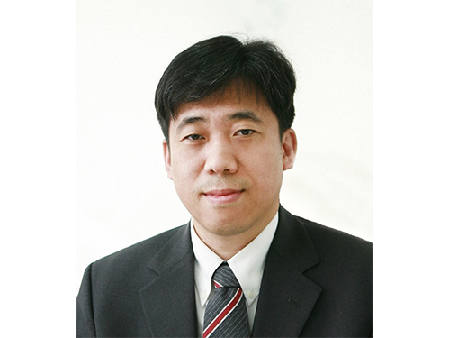 Professor Ki-Jun Jeong Wins the 2015 Dam Yeun Academic Award
The 11th Dam Yeun Academic Award presented by the Korean Society for Biotechnology and Bioengineering (KSBB) to a biologist under 45 years old went to Professor Ki-Jun Jeong of the Chemical and Biomolecular Engineering Department at KAIST.
The award ceremony took place on October 13, 2015, at the annual conference of KSBB held at Songdo Convensia in Incheon City.
Each year KSBB announces the recipient of the award based on the publications by researchers in the last five years at peer-reviewed international journals or KSBB Journal as well as the record of patent registration and technology transfers.
Professor Jeong is recognized for his pioneering research in protein, antibody, cellular engineering, and protein displays and chips.
2015.10.19 View 10746