materials
-
 KAIST Professors Selected as Y-KAST Members
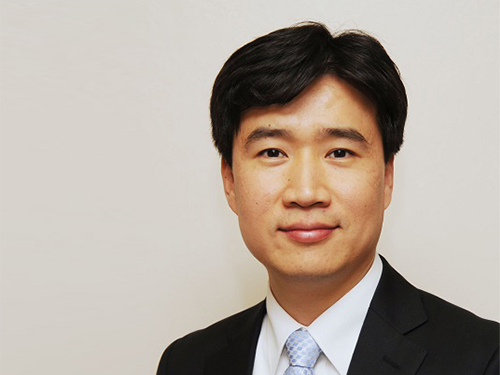
Professor YongKeun Park, Professor Bumjoon Kim, Professor Keon Jae Lee, and Professor Young Seok Ju were selected as the newest members of the Young Korean Academy of Science and Technology (Y-KAST).
The Korean Academy of Science and Technology, an academic institution of professional experts, selected 26 promising scientists under the age of 43 to join Y-KAST. and four KAIST professors were included in the list.
The newest members were conferred on February 26.
Research Field
Name
Natural Sciences
YongKeun Park (Dept. of Physics)
Engineering
Bumjoon Kim (Dept. of Chemical and Biomolecular Engineering)
Agricultural & Fishery Sciences
Keon Jae Lee (Dept. of Materials Science and Engineering)
Medical Sciences
Young Seok Ju (Graduate School of Medical Science and Engineering)
2018.03.05 View 9936
 -
 Professor Il-Doo Kim Recevies the Song-gok Award
Professor Il-Doo Kim from the Department of Materials Science and Engineering at KAIST received the 20th Song-gok Science and Technology Award from Korea Institute of Science and Technology (KSIT).
The Song-gok Science and Technology Award was established to praise the accomplishments of the first president, Hyung-seop Choi, whose penname is Song-gok. The award selects a recipient in the field of materials and technology every other year.
Professor Kim, in recognition of his outstanding research and contributions to materials science in Korea, received the award during the 52nd anniversary ceremony of KIST on February 9.
Professor Kim focuses on developing nanofiber gas sensors for diagnosing disease in advance by analyzing exhaled biomarkers with electrospinning technology.
He has published more than 211 papers and has recorded more than 9,650 citations and 50 h-index.
Professor Kim has registered 107 patents and applied 38 patents in Korea while registering 29 patents and applying 16 patents overseas. Also, he transferred four technologies in 2017.
Professor Kim is recognized as one of the researchers who is leading nanofiber technology. On January 17, he made a keynote speech at the 5th International Conference on Electrospinning, which was his fourth keynote speech at that conference.
Moreover, he received the Technology Innovation Award at the College of Engineering, KAIST on December 19, 2017.
Professor Kim said, “It is my great honor to receive the Song-gok Science and Technology Award. I would like to bring distinction to KAIST by taking the lead in the commercializing a nanofiber-based highly sensitive nanosensors, diversifying and commercializing technology using nanofiber.”
2018.02.13 View 9090
 -
 KAIST Students Invited to the BNL
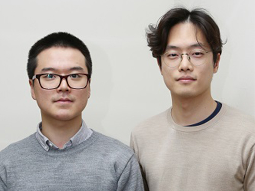
Siheon Ryee and Taek Jung Kim, combined Masters and PhD students from the Department of Physics, have been invited to be visiting researchers at the Brookhaven National Laboratory (BNL).
The BNL, located in Long Island, New York, is one of the most esteemed institutes in the United States. Ryee and Kim received the invitation from the Center for Computational Design of Functional Strongly Correlated Materials and Theoretical Spectroscopy. This center was established by scholars who have been leading this field in the United States.
The two students will be participating in developing a methodology and code for calculating strongly correlated electronic materials, and a grant of 40,000 USD will be provided to each student. This amount of support is not often awarded to researchers outside of postdoctoral programs.
Moreover, they are guaranteed to continue their combined Masters and PhD program and write their dissertations under the supervision of their advisor, Professor Myung Joon Han from the Department of Physics.
Professor Han said, “I was impressed by how well-known scholars established the center in order to cooperate with each other to solve challenging problems. Also, I was surprised and happy that my students were invited to this outstanding institute.”
“I believe that doing research with leaders in their field will give valuable experience to the students. At the same time, my students will be a great help to the scholars of the institute,” he added.
2018.01.11 View 8570
 -
 Ultra-Low Power Flexible Memory Using 2D Materials
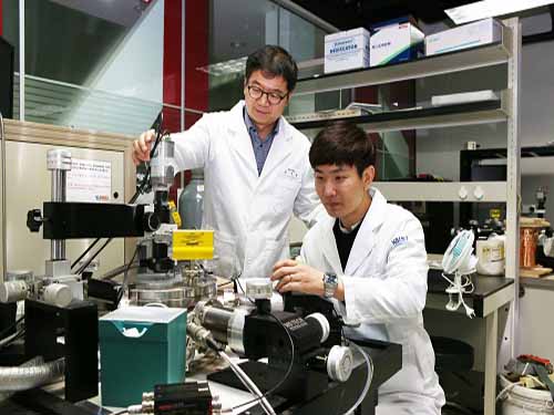
(Professor Choi and Ph.D. candidate Jang)
KAIST research team led by Professor Sung-Yool Choi at School of Electrical Engineering and Professor Sung Gap Im at the Department of Chemical and Biomolecular Engineering developed high-density, ultra-low power, non-volatile, flexible memory technology using 2D materials. The team used ultrathin molybdenum disulfide (MoS2) with atomic-scale thickness as the channel material and high-performance polymeric insulator film as the tunneling dielectric material. This research was published on the cover of Advanced Functional Materials on November 17. KAIST graduate Myung Hun Woo, a researcher at Samsung Electronics and Ph.D. candidate Byung Chul Jang are first authors.
The surge of new technologies such as Internet of Things (IoT), Artificial Intelligence (AI), and cloud server led to the paradigm shift from processor-centric computing to memory-centric computing in the industry, as well as the increase in demand of wearable devices. This led to an increased need for high-density, ultra-low power, non-volatile flexible memory. In particular, ultrathin MoS2 as semiconductor material has been recently regarded as post-silicon material. This is due to its ultrathin thickness of atomic-scale which suppresses short channel effect observed in conventional silicon material, leading to advantages in high- density and low-power consumption. Further, this thickness allows the material to be flexible, and thus the material is applicable to wearable devices.
However, due to the dangling-bond free surface of MoS2 semiconductor material, it is difficult to deposit the thin insulator film to be uniform and stable over a large area via the conventional atomic layer deposition process. Further, the currently used solution process makes it difficult to deposit uniformly low dielectric constant (k) polymeric insulator film with sub-10 nm thickness on a large area, thus indicating that the memory device utilizing the conventional solution-processed polymer insulator film cannot be operated at low-operating voltage and is not compatible with photolithography.
The research team tried to overcome the hurdles and develop high-density, ultra-low power, non-volatile flexible memory by employing a low-temperature, solvent-free, and all-dry vapor phase technique named initiated chemical vapor deposition (iCVD) process. Using iCVD process, tunneling polymeric insulator film with 10 nm thickness was deposited uniformly on MoS2 semiconductor material without being restricted by the dangling bond-free surface of MoS2. The team observed that the newly developed MoS2-based non-volatile memory can be operated at low-voltage (around 10V), in contrast to the conventional MoS2-based non-volatile memory that requires over 20V.
Professor Choi said, “As the basis for the Fourth Industrial revolution technologies including AI and IoT, semiconductor device technology needs to have characteristics of low-power and flexibility, in clear contrast to conventional memory devices.” He continued, “This new technology is significant in developing source technology in terms of materials, processes, and devices to contribute to achieve these characteristics.”
This research was supported by the Global Frontier Center for Advanced Soft Electronics and the Creative Materials Discovery Program by funded the National Research Foundation of Korea of Ministry of Science and ICT.
( Figure 1. Cover of Advanced Functional Materials)
(Figure 2. Concept map for the developed non-volatile memory material and high-resolution transmission electron microscopy image for material cross-section )
2018.01.02 View 9743
 -
 Professor Dai Gil Lee Recognized by the ICCS
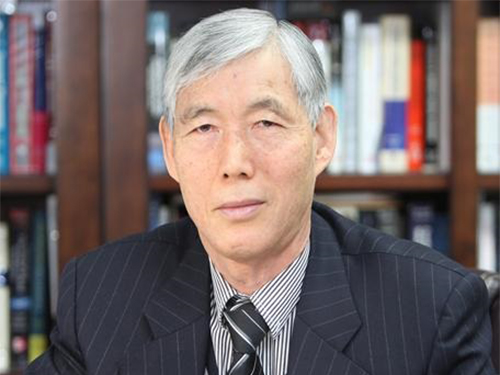
Emeritus Professor Dai Gil Lee, from the School of Mechanical and Aerospace Engineering at KAIST, received a special achievement award from the 20th International Conference on Composite Structures (ICCS).
ICCS is a renowned conference in the field of applied composite structures, which highlights the practicality of composite structures. This year, the conference was held at the Conservatoire National des Arts et Métiers (CNAM), Paris, France from September 4 to 7. Approximately 650 papers were presented from 45 countries.
Especially, the conference honored Emeritus Professor Lee, who has been engaged in ICCS since 1993 and received best paper award twice. The ICCS recognized him for serving with distinction in science and technology in the fields of composite materials and structures. As a member of the Editorial Board for many years, he gave significant support to the journal Composite Structures. At the conference, he gave a special lecture titled ‘Lightweight Carbon Composite Proton Exchange Membrane Fuel Cells’.
Professor Lee said, “I will dedicate myself to innovate Vanadium Redox Flow Battery-ESS (VRFB) based on the research findings announced at the conference and related patents. I am hoping that these efforts will contribute to solving energy issues around the world.”
2017.10.19 View 8555
 -
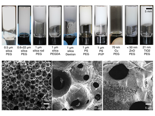 Processable High Internal Phase Pickering Emulsion Using Depletion Attraction
Professor Siyoung Choi’s research team from the KAIST Department of Chemical & Biomolecular Engineering used physical force to successfully produce a stable emulsion.
Emulsions, commonly known as cosmetic products, refer to stably dispersed structures of oil droplets in water (or water droplets in oil). Pickering emulsions refer to emulsions stabilized using solid particles, instead of detergent. Traditionally, it is said that water and oil do not mix. Until recently, detergent was added to mix oil and water for dispersion. Emulsions have traditionally been produced using this technique and are currently used for products such as mayonnaise, sun block, and lotion.
On the other hand, Pickering emulsions have been used after stabilization of chemical treatments on solid particle surfaces to enhance adsorption power. However, there were limitations in its application, since the treatment process is complex and its applicable range remains limited. Instead of chemical treatment on Pickering emulsion surfaces, the research team mixed small macromolecules a few nanometer in size with larger solid particles (tens of nanometers to a few micrometers). This induced depletion force was used to successfully stabilize the emulsion.
Depletion force refers to the force a large number of small particles induces to aggregate the bigger particles, in order to secure free space for themselves. In short, the force induces an attraction between larger particles. Until now, depletion force could only be applied to solids and solid particles. However, the research team used macromolecules and large particles such as solid particles and oil droplets to show the applicability of depletion force between solids and liquids. By introducing macromolecules that act as smaller particles, hydrophilic solid particles enhanced the adsorption of solid particles to the oil droplet surface, while preventing dissociation from the particle surface, resulting in the maintenance of a stable state.
The research team confirmed the possibility of the simple production of various porous macromolecular materials using stable Pickering emulsions. Such porous macromolecules are expected to be applicable in separation film, systems engineering, drug delivery, and sensors, given their large surface area.
Professor KyuHan Kim, the first author said, “Until now, depletion force has only been used between solid colloid particles. This research has scientific significance since it is the first example of using depletion force between solid particles and liquid droplets.”
Professor Choi said, “Beyond its academic significance, this technology could contribute to industries and national competitiveness.” He continued, “Since this technology uses physical force, not chemical, to produce stable emulsion, it can be used regardless of the type of solid particle and macromolecule. Further, it could be used in customized porous material production for special purposes.”
The research was published in Nature Communications online on February 1. In particular, this research is significant since an undergraduate student, Subeen Kim, participated in the project as a second author through the KAIST Undergraduate Research Program (URP). This research was funded by the National Research Foundation of Korea.
(Figure 1: Images of the inner structure of porous macromolecules produced using the new technology)
(Figure 2: Images showing the measurement of rheological properties of Pickering emulsions and system processability)
(Figure 3: Images showing a stable Pickering emulsion system)
2017.04.19 View 9424
 -
 Scholarship in Memory of Professor Shin Endowed by His Family
Professor Joong-Hoon Shin of the Graduate School of Nanoscience and Technology was touted as a genius young scientist who would take the lead in nanoscience technology. After earning degrees from Harvard and the Caltech, he was appointed at KAIST at age 27. He was the youngest professor ever appointed in Korea.
Professor Shin’s outstanding research in the field of semiconductor nano-optics led him to be named as the ‘Scientist of the Year’ for three consecutive years from 2004 by the most prestigious scientist and technology organizations including the Korean Academy Science and Technology, the National Research Foundation of Korea, and the Korean government. However, a fatal car accident last September on the way home from a seminar in Gangwon Province took his life and a promising scholar’s research was left unfinished. He was 47 years old.
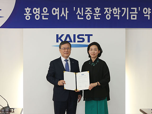
Mrs. Young-Eun Hong, the widow of the late Professor Shin, made a 100 million KRW gift to KAIST to establish the ‘Joong-Hoon Shin Scholarship’ on April 7. The scholarship will provide financial assistance to outstanding students of physics and nanoscience.
At the donation ceremony attended by President Sung-Chul Shin, Professor Shin’s colleagues and students, and family members, Mrs. Hong said, “My family would like to help young students achieve their dreams on behalf of my husband. I hope students will remember my husband’s passion and dedication toward his studies for a long time. He was a very hard worker.”
Working at KAIST, Professor Shin made significant achievements in field of semiconductor nano-optics, specializing in silicon photonics and silicon nanocrystal structures. In particular, his research team gained attention reproducing the structure of ‘Morpho butterfly’ wings, which produce the same colors from various angles, using external light as a light source without extra power. Their research led to the creation of original technology dubbed the biomimetics reflective display and was published in Nature in 2012.
Professor Shin’s legacy still endures. In February, a research team under Professor Shin-Hyun Kim of the Department of Chemical and Biomolecular Engineering includingthe late Professor Shin’s doctoral student Seung Yeol Lee, posthumously dedicated their research published on Advanced Materials to Professor Shin. ( click )
KAIST President Sung-Chul Shin, who is also a physicist, said “His passing is a great loss to the whole scientific and technology community, at home and abroad. But Joong-Hoon Shin scholarship will enable the growth and ensure the strength of nanoscience and its education at KAIST. We will uphold Professor Shin’s legacy by doing our best to make KAIST a world-leading university which can create global value.”
Mrs. Hong said she will continue her husband’s academic legacy at his alma maters, Harvard and the Caltech, where he earned his BS in physics and his Ph.D. in applied physics respectively. She said she will start fundraising to establish the Joong-Hoon Shin Scholarship at Harvard and Caltech from July.
(Mrs. Hong poses with President Sung-Chul Shin after donating 100 million KRW for establishing 'Joong-Hoon Shin Scholarship' in memory of her husband on April 7.)
2017.04.10 View 8434
 -
 Improving Silver Nanowires for FTCEs with Flash Light Interactions
Flexible transparent conducting electrodes (FTCEs) are an essential element of flexible optoelectronics for next-generation wearable displays, augmented reality (AR), and the Internet of Things (IoTs). Silver nanowires (Ag NWs) have received a great deal of attention as future FTCEs due to their great flexibility, material stability, and large-scale productivity. Despite these advantages, Ag NWs have drawbacks such as high wire-to-wire contact resistance and poor adhesion to substrates, resulting in severe power consumption and the delamination of FTCEs.
A research team led by Professor Keon Jae Lee of the Materials Science and Engineering Department at KAIST and Dr. Hong-Jin Park from BSP Inc., has developed high-performance Ag NWs (sheet resistance ~ 5 Ω/sq, transmittance 90 % at λ = 550 nm) with strong adhesion on plastic (interfacial energy of 30.7 J∙m-2) using flash light-material interactions.
The broad ultraviolet (UV) spectrum of a flash light enables the localized heating at the junctions of nanowires (NWs), which results in the fast and complete welding of Ag NWs. Consequently, the Ag NWs demonstrate six times higher conductivity than that of the pristine NWs. In addition, the near-infrared (NIR) of the flash lamp melted the interface between the Ag NWs and a polyethylene terephthalate (PET) substrate, dramatically enhancing the adhesion force of the Ag NWs to the PET by 310 %.
Professor Lee said, “Light interaction with nanomaterials is an important field for future flexible electronics since it can overcome thermal limit of plastics, and we are currently expanding our research into light-inorganic interactions.”
Meanwhile, BSP Inc., a laser manufacturing company and a collaborator of this work, has launched new flash lamp equipment for flexible applications based on the Professor Lee’s research.
The results of this work entitled “Flash-Induced Self-Limited Plasmonic Welding of Ag NW Network for Transparent Flexible Energy Harvester (DOI: 10.1002/adma.201603473)” were published in the February 2, 2017 issue of Advanced Materials as the cover article.
Professor Lee also contributed an invited review in the same journal of the April 3, 2017 online issue, “Laser-Material Interactions for Flexible Applications (DOI:10.1002/adma.201606586),” overviewing the recent advances in light interactions with flexible nanomaterials.
References
[1] Advanced Materials, February 2, 2017, Flash-Induced Self-Limited Plasmonic Welding of Ag NW network for Transparent Flexible Energy Harvester http://onlinelibrary.wiley.com/doi/10.1002/adma.201603473/epdf
[2] Advanced Materials, April 3, 2017, Laser-Material Interactions for Flexible Applications
http://onlinelibrary.wiley.com/doi/10.1002/adma.201606586/abstract
For further inquiries on research:
keonlee@kaist.ac.kr (Keon Jae Lee), hjpark@bsptech.co.kr (Hong-Jin Park)
Picture 1: Artistic Rendtition of Light Interaction with Nanomaterials
(This image shows flash-induced plasmonic interactions with nanowires to improve silver nanowires (Ag NWs).)
Picture 2: Ag NW/PET Film
(This picture shows the Ag NWs on a polyethylene terephthalate (PET) film after the flash-induced plasmonic thermal process.)
2017.04.05 View 11121
 -
 Highly-Efficient Photoelectrochemical CO2 Reduction
Direct CO2 conversion has continuously attracted a great deal of attention as a technology to produce fuels and chemical building blocks from renewable energy resources. Specifically, substances such as carbon feedstocks and fuels can be produced by utilizing sunlight, water, and CO2 as semiconductors and a water interface through photoelectrochemical CO2 reduction.
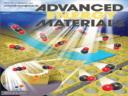
A KAIST research team demonstrated a novel photoelectrode structure for highly-selective and efficient photoelectrochemical CO2 reduction reactions. The research team led by Professor Jihun Oh of the Graduate School of EEWS (Energy, Environment, Water and Sustainability) presented a Si photoelectrode with a nanoporous Au thin film that is capable of reducing CO2 to CO with 90 percent selectivity in aqueous solution. The research team’s technology will provide a basic framework for designing the semiconductor photoelectrode structure necessary for photoelectrochemical conversion.
In order to achieve steady conversion of CO2, it is necessary to use a high-performance catalyst to lower overpotential. Among the metal catalysts, Au is known to be an electrocatalyst that converts CO2 to CO.
Conventionally, bare Au, as a catalyst, produces a lot of hydrogen gas due to its low CO selectivity. In addition, the high cost of Au remains a challenge in using the catalyst. Professor Oh’s research team addressed the issue by creating a nanoporous Au thin film formed by the electrochemical reduction of an anodized Au thin film.
As a result, the team could demonstrate an efficient, selective photoelectrochemical reduction reaction of CO2 to CO using electrochemically-treated Au thin films on a Si photoelectrode. The electrochemical reduction on anodized Au thin films forms a nanoporous thin layer exhibiting many grain boundaries of nanoparticles on the Au surface. This dramatically improves the selectivity of the reduction reaction with a maximum CO faradaic efficiency of over 90% at low overpotential and durability.
The research team also used an Au thin film of about 200 nanometers, 50,000 times thinner than previously reported nanostructured Au catalysts, resulting in a cost-effective catalyst. When depositing the catalyst on the semiconductor surface in the type of nanoparticles, the substrate of the thin film will be affected in the course of electrochemical reduction.
Thus, the research team designed a new Si photoelectrode with mesh-type co-catalysts that are independently wired at the front and back of the photoelectrode without influencing the photoelectrode, and made it possible for electrochemical reduction.
Due to the superior CO2 reduction reaction activity of the nanoporous Au mesh and high photovoltage from Si, the Si photoelectrode with the nanoporous Au thin film mesh shows conversion of CO2 to CO with 91% Faradaic efficiency at positive potential than CO equilibrium potential.
Professor Oh explained, “This technology will serve as a platform for diverse semiconductors and catalysts. Researchers can further improve the solar-to-CO2 conversion efficiency using this technology.
Dr. Jun Tae Song, the first author continued, “This new approach made it possible to develop a simple but very important type of electrode structure. It is the first time to achieve CO2 conversion at the potential lower than equilibrium potential. We believe that our research will contribute to efficient CO2 conversion.”
This research was published in the inside front cover of Advanced Energy Materials on February 8, 2017. The research was funded and supported by the Korea Carbon Capture & Sequestration R&D Center. Professor Sung-Yoon Chung of the EEWS also participated in this research.
(Figure: Schematic diagram of a Si photoelectrode that patterns with mesh-type nanoporous Au)
2017.03.08 View 10246
 -
 Semiconductor Photonic Nanocavities on Paper Substrates
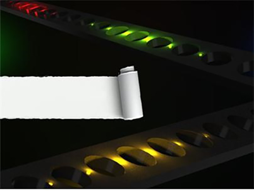
Professor Yong-Hoon Cho of the Department of Physics and his team at KAIST have developed a semiconductor photonic nanocavity laser that can operate on a paper substrate.
The researchers hope that this novel method, which involves transferring nano-sized photonic crystal particles onto a paper substrate with high absorptiveness, will enable the diagnoses of various diseases by using high-tech semiconductor sensors at low cost.
The results of this research were published in the November 17th, 2016, issue of Advanced Materials.
Photonic crystals, which utilize light as a medium to provide high bandwidths, can transfer large amounts of information. Compared with their electronic counterparts, photonic crystals also consume less energy to operate.
Normally, semiconductor photonic particles require substrates, which play only a passive role in the assembly and endurance of individual, functional photonic components. These substrates, however, are bulky and environmentally hazardous as they are made up of non-biodegradable materials.
The research team overcame these two shortcomings by replacing a semiconductor substrate with standard paper. The substrate’s mass was reduced considerably, and because paper is made from trees, it degrades. Paper can be easily and cheaply acquired from our surroundings, which drastically reduces the unit cost of semiconductors.
In addition, paper possesses superior mechanical characteristics. It is flexible and can be repeatedly folded and unfolded without being torn. These are traits that have long been sought by researchers for existing flexible substrates.
The research team used a micro-sized stamp to detach photonic crystal nanobeam cavities selectively from their original substrate and transfer them onto a new paper substrate. Using this technique, the team removed nanophotonic crystals that had been patterned (using a process of selectively etching circuits onto a substrate) onto a semiconductor substrate with a high degree of integration, and realigned them as desired on a paper substrate.
The nanophotonic crystals that the team combined with paper in this research were 0.5 micrometers in width, 6 micrometers in length, and 0.3 micrometers in height—about one-hundredth of the width of a single hair (0.1 millimeter).
The team also transferred their photonic crystals onto paper with a fluid channel, which proved that it could be used as a refractive index sensor. As can be seen in current commercial pregnancy diagnosis kits, paper has high absorptiveness. Since photonic crystal particles have high sensitivity, they are highly suitable for applications such as sensors.
Professor Cho stated that “by using paper substrates, this technology can greatly contribute to the rising field of producing environmentally-friendly photonic particles” and “by combining inexpensive paper and high-performance photonic crystal sensors, we can obtain low prices as well as designing appropriate technologies with high performance.”
Dr. Sejeong Kim of the Department of Physics participated in this study as the first author, and Professor Kwanwoo Shin of Sogang University and Professor Yong-Hee Lee of KAIST also took part in this research. The research was supported by the National Research Foundation’s Mid-Career Researcher Program, and the Climate Change Research Hub of KAIST.
Figure 1. Illustration of photonic crystal lasers on paper substrates
Figure 2. Photonic crystal resonator laser and refractive index sensor operating on paper substrates
2017.03.01 View 7853
 -
 EEWS Graduate School Team Receives the S-Oil Best Paper Award
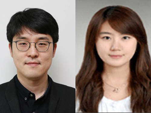
Professor Hyungjun Kim and Dr. He-Young Shin from the EEWS (Energy, Environment, Water and Sustainability) Graduate School at KAIST received the Best Paper Award in Chemistry from S-Oil, a Korean petroleum and refinery company, on November 29, 2016.
Established in 2011, the S-Oil Best Paper Awards are bestowed annually upon ten young scientists in the fields of five basic sciences: mathematics, physics, chemistry, biology, and earth science. The scientists are selected at the recommendation of the Korean Academy of Science and Technology and the Association of Korean Universities. The awards grant a total of USD 230,000 for research funding.
Dr. Shin, the lead author of the awarded research paper, said, “My research interest has been catalyst studies based on theoretical chemistry. I am pleased to accept this award that will support my studies, and will continue to research catalyst design that can predict parameters and integrate them into catalytic systems.”
Professor Hyungjun Kim (left) and Dr. He-Young Shin (right)
2016.12.23 View 11005
 -
 Extremely Thin and Highly Flexible Graphene-Based Thermoacoustic Speakers
A joint research team led by Professors Jung-Woo Choi and Byung Jin Cho of the School of Electrical Engineering and Professor Sang Ouk Kim of the Material Science and Engineering Department, all on the faculty of the Korea Advanced Institute of Science and Technology (KAIST), has developed a simpler way to mass-produce ultra-thin graphene thermosacoustic speakers.
Their research results were published online on August 17, 2016 in a journal called Applied Materials & Interfaces. The IEEE Spectrum, a monthly magazine published by the Institute of Electrical and Electronics Engineers, reported on the research on September 9, 2016, in an article titled, “Graphene Enables Flat Speakers for Mobile Audio Systems.” The American Chemical Society also drew attention to the team’s work in its article dated September 7, 2016, “Bringing Graphene Speakers to the Mobile Market.”
Thermoacoustic speakers generate sound waves from temperature fluctuations by rapidly heating and cooling conducting materials. Unlike conventional voice-coil speakers, thermoacoustic speakers do not rely on vibrations to produce sound, and thus do not need bulky acoustic boxes to keep complicated mechanical parts for sound production. They also generate good quality sound in all directions, enabling them to be placed on any surface including curved ones without canceling out sounds generated from opposite sides.
Based on a two-step, template-free fabrication method that involved freeze-drying a solution of graphene oxide flakes and the reduction/doping of oxidized graphene to improve electrical properties, the research team produced a N-doped, three-dimensional (3D), reduced graphene oxide aerogel (N-rGOA) with a porous macroscopic structure that permitted easy modulation for many potential applications.
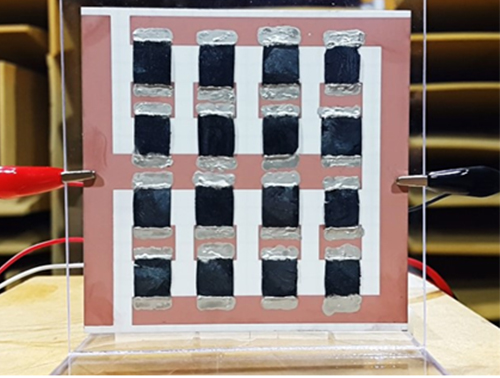
Using 3D graphene aerogels, the team succeeded in fabricating an array of loudspeakers that were able to withstand over 40 W input power and that showed excellent sound pressure level (SPL), comparable to those of previously reported 2D and 3D graphene loudspeakers.
Choong Sun Kim, the lead author of the research paper and a doctoral student in the School of Electrical Engineering at KAIST, said:
“Thermoacoustic speakers have a higher efficiency when conducting materials have a smaller heat capacity. Nanomaterials such as graphene are an ideal candidate for conductors, but they require a substrate to support their extremely thinness. The substrate’s tendency to lose heat lowers the speakers’ efficiency. Here, we developed 3D graphene aerogels without a substrate by using a simple two-step process. With graphene aerogels, we have fabricated an array of loudspeakers that demonstrated stable performance. This is a practical technology that will enable mass-production of thermosacoustic speakers including on mobile platforms.”
The research paper is entitled “Application of N-Doped Three-Dimensional Reduced Graphene Oxide Aerogel to Thin Film Loudspeaker.” (DOI: 10.1021/acsami.6b03618)
Figure 1: A Thermoacoustic Loudspeaker Consisted of an Array of 16 3D Graphene Aerogels
Figure 2: Two-step Fabrication Process of 3D Reduced Graphene Oxide Aerogel Using Freeze-Drying and Reduction/Doping
Figure 3: X-ray Photoelectron Spectroscopy Graph of the 3D Reduced Graphene Oxide Aerogel and Its Scanning Electron Microscope Image
2016.10.05 View 14504