Department+of+materials+science
-
 High-resolution Atomic Imaging of Specimens in Liquid Observed by Transmission Electron Microscopes Using Graphene Liquid Cells
Looking into specimens in liquid at the atomic level to understand nanoscale processes so far regarded as impossible to witnessThe Korea Advanced Institute of Science and Technology (KAIST) announced that a research team from the Department of Materials Science and Engineering has developed a technology that enables scientists and engineers to observe processes occurring in liquid media on the smallest possible scale which is less than a nanometer.
Professor Jeong Yong Lee and Researcher Jong Min Yuk, in collaboration with Professors Paul Alivisatos’s and Alex Zettl’s groups at the University of California, Berkeley, succeeded in making a graphene liquid cell or capsule, confining an ultra-thin liquid film between layers of graphene, for real-time and in situ imagining of nanoscale processes in fluids with atomic-level resolution by a transmission electron microscope (TEM). Their research was published in the April 6, 2012 issue of Science. (http://www.sciencemag.org/content/336/6077/61.abstract)
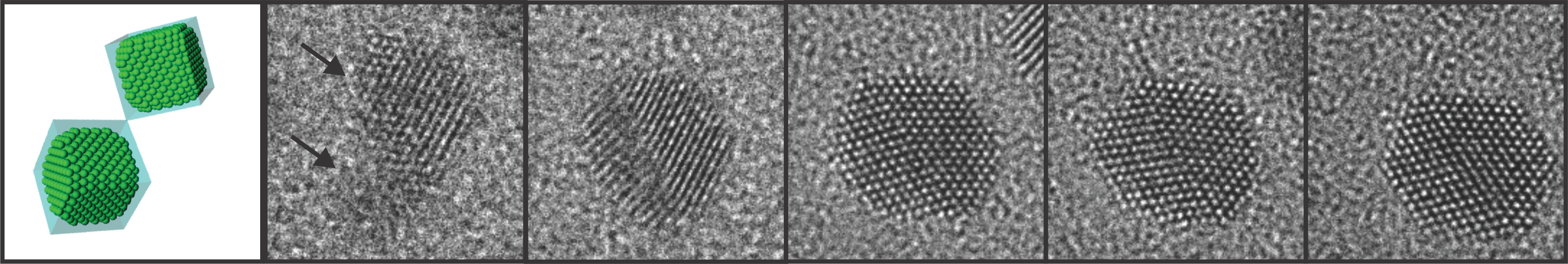
The graphene liquid cell (GLC) is composed of two sheets of graphene sandwiched to create a sealed chamber where a platinum growth solution is encapsulated in the form of a thin slice. Each graphene layer has a thickness of one carbon atom, the thinnest membrane that has ever been used to fabricate a liquid cell required for TEM.
The research team peered inside the GLC to observe the growth and dynamics of platinum nanocrystals in solution as they coalesced into a larger size, during which the graphene membrane with the encapsulated liquid remained intact. The researchers from KAIST and the UC Berkeley identified important features in the ongoing process of the nanocrystals’ coalescence and their expansion through coalescence to form certain shapes by imaging the phenomena with atomic-level resolution.
Professor Lee said,
“It has now become possible for scientists to observe what is happening in liquids on an atomic level under transmission electron microscopes.”
Researcher Yuk, one of the first authors of the paper, explained his research work.
“This research will promote other fields of study related to materials in a fluid stage including physical, chemical, and biological phenomena at the atomic level and promises numerous applications in the future. Pending further studies on liquid microscopy, the full application of a graphene-liquid-cell (GLC) TEM to biological samples is yet to be confirmed. Nonetheless, the GLC is the most effective technique developed today to sustain the natural state of fluid samples or species suspended in the liquid for a TEM imaging.”
The transmission electron microscope (TEM), first introduced in the 1930s, produces images at a significantly higher resolution than light microscopes, allowing users to examine the smallest level of physical, chemical, and biological phenomena. Observations by TEM with atomic resolution, however, have been limited to solid and/or frozen samples, and thus it has previously been impossible to study the real time fluid dynamics of liquid phases.
TEM imaging is performed in a high vacuum chamber in which a thin slice of the imaged sample is situated, and an electron beam passes through the slice to create an image. In this process, a liquid medium, unlike solid or frozen samples, evaporates, making it difficult to observe under TEM.
Attempts to produce a liquid capsule have thus far been made with electron-transparent membranes of such materials as silicon nitride or silicon oxide; such liquid capsules are relatively thick (tens to one hundred nanometers), however, resulting in poor electron transmittance with a reduced resolution of only a few nanometers. Silicon nitride is 25 nanometers thick, whereas graphene is only 0.34 nanometers.
Graphene, most commonly found in bulk graphite, is the thinnest material made out of carbon atoms. It has unique properties such as mechanical tensile strength, high flexibility, impermeability to small molecules, and high electrical conductivity. Graphene is an excellent material to hold micro- and nanoscopic objects for observation in a transmission electron microscope by minimizing scattering of the electron beam that irradiates a liquid sample while reducing charging and heating effects.
###
Figure 1. Schematic illustration of graphene liquid cells. Sandwiched two sheets of graphene encapsulate a platinum growth solution.
Figure 2. In-situ TEM observation of nanocrystal growth and shape evolution. TEM images of platinum nanocrystal coalescence and their faceting in the growth solution.
2012.04.23 View 13643
High-resolution Atomic Imaging of Specimens in Liquid Observed by Transmission Electron Microscopes Using Graphene Liquid Cells
Looking into specimens in liquid at the atomic level to understand nanoscale processes so far regarded as impossible to witnessThe Korea Advanced Institute of Science and Technology (KAIST) announced that a research team from the Department of Materials Science and Engineering has developed a technology that enables scientists and engineers to observe processes occurring in liquid media on the smallest possible scale which is less than a nanometer.
Professor Jeong Yong Lee and Researcher Jong Min Yuk, in collaboration with Professors Paul Alivisatos’s and Alex Zettl’s groups at the University of California, Berkeley, succeeded in making a graphene liquid cell or capsule, confining an ultra-thin liquid film between layers of graphene, for real-time and in situ imagining of nanoscale processes in fluids with atomic-level resolution by a transmission electron microscope (TEM). Their research was published in the April 6, 2012 issue of Science. (http://www.sciencemag.org/content/336/6077/61.abstract)
The graphene liquid cell (GLC) is composed of two sheets of graphene sandwiched to create a sealed chamber where a platinum growth solution is encapsulated in the form of a thin slice. Each graphene layer has a thickness of one carbon atom, the thinnest membrane that has ever been used to fabricate a liquid cell required for TEM.
The research team peered inside the GLC to observe the growth and dynamics of platinum nanocrystals in solution as they coalesced into a larger size, during which the graphene membrane with the encapsulated liquid remained intact. The researchers from KAIST and the UC Berkeley identified important features in the ongoing process of the nanocrystals’ coalescence and their expansion through coalescence to form certain shapes by imaging the phenomena with atomic-level resolution.
Professor Lee said,
“It has now become possible for scientists to observe what is happening in liquids on an atomic level under transmission electron microscopes.”
Researcher Yuk, one of the first authors of the paper, explained his research work.
“This research will promote other fields of study related to materials in a fluid stage including physical, chemical, and biological phenomena at the atomic level and promises numerous applications in the future. Pending further studies on liquid microscopy, the full application of a graphene-liquid-cell (GLC) TEM to biological samples is yet to be confirmed. Nonetheless, the GLC is the most effective technique developed today to sustain the natural state of fluid samples or species suspended in the liquid for a TEM imaging.”
The transmission electron microscope (TEM), first introduced in the 1930s, produces images at a significantly higher resolution than light microscopes, allowing users to examine the smallest level of physical, chemical, and biological phenomena. Observations by TEM with atomic resolution, however, have been limited to solid and/or frozen samples, and thus it has previously been impossible to study the real time fluid dynamics of liquid phases.
TEM imaging is performed in a high vacuum chamber in which a thin slice of the imaged sample is situated, and an electron beam passes through the slice to create an image. In this process, a liquid medium, unlike solid or frozen samples, evaporates, making it difficult to observe under TEM.
Attempts to produce a liquid capsule have thus far been made with electron-transparent membranes of such materials as silicon nitride or silicon oxide; such liquid capsules are relatively thick (tens to one hundred nanometers), however, resulting in poor electron transmittance with a reduced resolution of only a few nanometers. Silicon nitride is 25 nanometers thick, whereas graphene is only 0.34 nanometers.
Graphene, most commonly found in bulk graphite, is the thinnest material made out of carbon atoms. It has unique properties such as mechanical tensile strength, high flexibility, impermeability to small molecules, and high electrical conductivity. Graphene is an excellent material to hold micro- and nanoscopic objects for observation in a transmission electron microscope by minimizing scattering of the electron beam that irradiates a liquid sample while reducing charging and heating effects.
###
Figure 1. Schematic illustration of graphene liquid cells. Sandwiched two sheets of graphene encapsulate a platinum growth solution.
Figure 2. In-situ TEM observation of nanocrystal growth and shape evolution. TEM images of platinum nanocrystal coalescence and their faceting in the growth solution.
2012.04.23 View 13643 -
 A Step Closer to Ultra Slim Mobile Phone
Professor Baek Kyung Wook (department of Material Science and Engineering) succeeded in developing an ultra-thin conjugation technique that can perfectly replace the modular contact in electronic devices.
The research team developed a compound material using ultra-fine solder-adhesive film and developed the vertical ultrasonic conjugation process thereby making a reliable utra-thin conjugation.
The developed technique allowed for very thin and reliable conjugation and will be able to replace the socket type connector and is expected to revolutionize the electronic device industry.
In mobile electronic devices like the smartphone, the trend is to incorporate various functional modules like camera, display, touchscreens, etc. in addition to striving for miniaturization of the device.
Recently the problem was the fact that the number of modules within the device was increasing due to the incorporation of various functions, and consequently the volume that these modules took up increased as well, which made miniaturization almost impossible.
Professor Baek‘s team succeeded in improving upon this problem by creating a compound material that has ultra-fine solder particles that can melt to form alloy fusion with the electrode and thermosetting adhesive film that can wrap around the electrode and provide mechanical protection.
The use of this material made it possible to reduce the thickness of the connector by hundredth fold which improved electrical, mechanical properties and highly reliable.
From a processing standpoint the conventional conjugation process involved heating the mechanical block and was therefore hard to manage its production and also consumed 1000W and took up to 15 seconds.
By contrast, Professor Baek’s team’s new process uses only ultrasound to locally heat and melt the conjugation point itself thereby reducing power consumption to 100W and conjugation time to 1~5 seconds.
The technique developed by Professor Baek and Lee Ki Won Doctorate student was awarded Excellent Dissertation Award by world famous journals like the Electronic Components and Technology Conference and is being recognized worldwide.
2012.01.31 View 12039
A Step Closer to Ultra Slim Mobile Phone
Professor Baek Kyung Wook (department of Material Science and Engineering) succeeded in developing an ultra-thin conjugation technique that can perfectly replace the modular contact in electronic devices.
The research team developed a compound material using ultra-fine solder-adhesive film and developed the vertical ultrasonic conjugation process thereby making a reliable utra-thin conjugation.
The developed technique allowed for very thin and reliable conjugation and will be able to replace the socket type connector and is expected to revolutionize the electronic device industry.
In mobile electronic devices like the smartphone, the trend is to incorporate various functional modules like camera, display, touchscreens, etc. in addition to striving for miniaturization of the device.
Recently the problem was the fact that the number of modules within the device was increasing due to the incorporation of various functions, and consequently the volume that these modules took up increased as well, which made miniaturization almost impossible.
Professor Baek‘s team succeeded in improving upon this problem by creating a compound material that has ultra-fine solder particles that can melt to form alloy fusion with the electrode and thermosetting adhesive film that can wrap around the electrode and provide mechanical protection.
The use of this material made it possible to reduce the thickness of the connector by hundredth fold which improved electrical, mechanical properties and highly reliable.
From a processing standpoint the conventional conjugation process involved heating the mechanical block and was therefore hard to manage its production and also consumed 1000W and took up to 15 seconds.
By contrast, Professor Baek’s team’s new process uses only ultrasound to locally heat and melt the conjugation point itself thereby reducing power consumption to 100W and conjugation time to 1~5 seconds.
The technique developed by Professor Baek and Lee Ki Won Doctorate student was awarded Excellent Dissertation Award by world famous journals like the Electronic Components and Technology Conference and is being recognized worldwide.
2012.01.31 View 12039 -
 Cancer detection from an implantable, flexible LED
Professor Keon Jae Lee
A KAIST research team has developed a new type of biocompatible and bendable GaN LED biosensor.
Daejeon, the Republic of Korea, August 8, 2011—Can a flexible LED conformably placed on the human heart, situated on the corrugated surface of the human brain, or rolled upon the blood vessels, diagnose or even treat various diseases? These things might be a reality in the near future.
The team of Professor Keon Jae Lee (Department of Materials Science and Engineering, KAIST) has developed a new concept: a biocompatible, flexible Gallium Nitride (GaN) LED that can detect prostate cancer.
GaN LED, a highly efficient light emitting device, has been commercialized in LED TVs and in the lighting industry. Until now, it has been difficult to use this semiconductor material to fabricate flexible electronic systems due to its brittleness. The research team, however, has succeeded in developing a highly efficient, flexible GaN LED and in detecting cancer using a flexible LED biosensor.
Prof. Lee was involved in the first co-invention of "High Performance Flexible Single Crystal GaN" during his PhD course at the University of Illinois at Urbana-Champaign (UIUC). This flexible GaN LED biosensor utilized a similar protocol to transfer thin GaN LED films onto flexible substrates, followed by a biocompatible packaging process; the system’s overall potential for use in implantable biomedical applications was demonstrated.
Professor John Roger (Department of Materials Science and Engineering, UIUC) said,
“Bio-integrated LEDs represent an exciting, new technology with strong potential to address important challenges in human health. This present work represents a very nice contribution to this emerging field.”
This paper was published in the online issue of Nano Energy Elsevier Journal (Editor, Prof. Zhong Lin Wang) dated September 16, 2011.
Flexible GaN LED produces blue light.
2011.09.20 View 14209
Cancer detection from an implantable, flexible LED
Professor Keon Jae Lee
A KAIST research team has developed a new type of biocompatible and bendable GaN LED biosensor.
Daejeon, the Republic of Korea, August 8, 2011—Can a flexible LED conformably placed on the human heart, situated on the corrugated surface of the human brain, or rolled upon the blood vessels, diagnose or even treat various diseases? These things might be a reality in the near future.
The team of Professor Keon Jae Lee (Department of Materials Science and Engineering, KAIST) has developed a new concept: a biocompatible, flexible Gallium Nitride (GaN) LED that can detect prostate cancer.
GaN LED, a highly efficient light emitting device, has been commercialized in LED TVs and in the lighting industry. Until now, it has been difficult to use this semiconductor material to fabricate flexible electronic systems due to its brittleness. The research team, however, has succeeded in developing a highly efficient, flexible GaN LED and in detecting cancer using a flexible LED biosensor.
Prof. Lee was involved in the first co-invention of "High Performance Flexible Single Crystal GaN" during his PhD course at the University of Illinois at Urbana-Champaign (UIUC). This flexible GaN LED biosensor utilized a similar protocol to transfer thin GaN LED films onto flexible substrates, followed by a biocompatible packaging process; the system’s overall potential for use in implantable biomedical applications was demonstrated.
Professor John Roger (Department of Materials Science and Engineering, UIUC) said,
“Bio-integrated LEDs represent an exciting, new technology with strong potential to address important challenges in human health. This present work represents a very nice contribution to this emerging field.”
This paper was published in the online issue of Nano Energy Elsevier Journal (Editor, Prof. Zhong Lin Wang) dated September 16, 2011.
Flexible GaN LED produces blue light.
2011.09.20 View 14209