Engineering
-
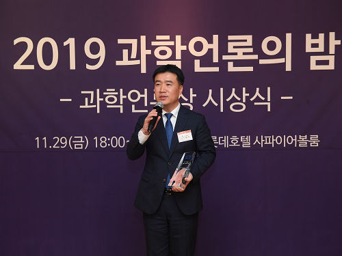 Professor Il-Doo Kim Named Scientist of the Year by the Journalists
Professor Il-Doo Kim from the Department of Materials Science and Engineering was named the 2019 Scientist of the Year by Korean science journalists. The award was conferred at the 2019 Science Press Night ceremony of the Korea Science Journalists Association (KSJA) on November 29.
Professor Kim focuses on developing nanofiber gas sensors for diagnosing diseases in advance by analyzing exhaled biomarkers with electrospinning technology. His outstanding research was praised and selected as one of the top 10 nanotechnology of 2019 by the Korea Nano Technology Research Society (KoNTRS), the Ministry of Science and ICT (MSIT), and the Ministry of Trade, Industry and Energy (MOTIE).
Professor Kim was honored with the QIAN Baojun Fiber Award, which is awarded every two years by Donghua University in Shanghai, China to recognize outstanding contributions in fiber science and technology. Professor Kim was also elected as an academician of the Asia Pacific Academy of Materials (APAM) on November 21 in Guangzhou, China.
In May, Professor Kim was appointed as an associate editor of ACS Nano, a leading international research journal in the field of nanoscience. In his editorial published in the May issue of ACS Nano, Professor Kim introduced and shared the history of KAIST and its vision for the future with other members of the journal. He hopes this will help with promoting a closer relationship between the members of the journal and KAIST moving forward.
“Above all,” he said in his acceptance speech, “the greatest news for me as an educator is that the first PhD graduate from our lab, Dr. Seonjin Choi, was appointed as the youngest professor in the Division of Materials Science and Engineering at Hanyang University on September 1.”
2019.12.17 View 12258
 -
 KAIST and Google Jointly Develop AI Curricula
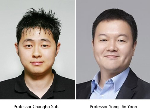
KAIST selected the two professors who will develop AI curriculum under the auspices of the KAIST-Google Partnership for AI Education and Research. The Graduate School of AI announced the two authors among the 20 applicants who will develop the curriculum next year. They will be provided 7,500 USD per subject.
Professor Changho Suh from the School of Electrical Engineering and Professor Yong-Jin Yoon from the Department of Mechanical Engineering will use Google technology such as TensorFlow, Google Cloud, and Android to create the curriculum.
Professor Suh’s “TensorFlow for Information Theory and Convex Optimization “will be used for curriculum in the graduate courses and Professor Yoon’s “AI Convergence Project Based Learning (PBL)” will be used for online courses. Professor Yoon’s course will explore and define problems by utilizing AI and experiencing the process of developing products that use AI through design thinking, which involves product design, production, and verification. Professor Suh’s course will discus“information theory and convergence,” which uses basic sciences and engineering as well as AI, machine learning, and deep learning.
2019.12.04 View 15281
 -
 ‘Carrier-Resolved Photo-Hall’ to Push Semiconductor Advances
(Professor Shin and Dr. Gunawan (left))
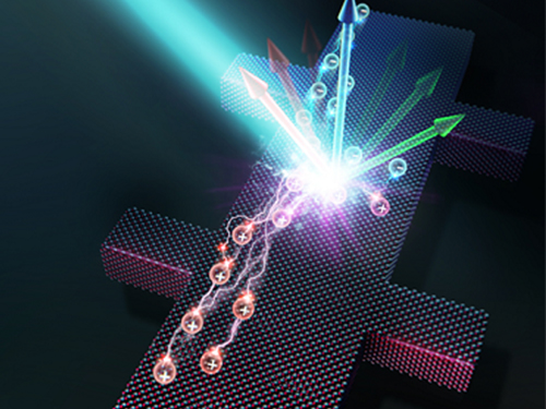
An IBM-KAIST research team described a breakthrough in a 140-year-old mystery in physics. The research reported in Nature last month unlocks the physical characteristics of semiconductors in much greater detail and aids in the development of new and improved semiconductor materials.
Research team under Professor Byungha Shin at the Department of Material Sciences and Engineering and Dr. Oki Gunawan at IBM discovered a new formula and technique that enables the simultaneous extraction of both majority and minority carrier information such as their density and mobility, as well as gain additional insights about carrier lifetimes, diffusion lengths, and the recombination process. This new discovery and technology will help push semiconductor advances in both existing and emerging technologies.
Semiconductors are the basic building blocks of today’s digital electronics age, providing us with a multitude of devices that benefit our modern life. To truly appreciate the physics of semiconductors, it is very important to understand the fundamental properties of the charge carriers inside the materials, whether those particles are positive or negative, their speed under an applied electric field, and how densely they are packed into the material.
Physicist Edwin Hall found a way to determine those properties in 1879, when he discovered that a magnetic field will deflect the movement of electronic charges inside a conductor and that the amount of deflection can be measured as a voltage perpendicular to the flow of the charge. Decades after Hall’s discovery, researchers also recognized that they can measure the Hall effect with light via “photo-Hall experiments”. During such experiments, the light generates multiple carriers or electron–hole pairs in the semiconductors.
Unfortunately, the basic Hall effect only provided insights into the dominant charge carrier (or majority carrier). Researchers were unable to extract the properties of both carriers (the majority and minority carriers) simultaneously. The property information of both carriers is crucial for many applications that involve light such as solar cells and other optoelectronic devices.
In the photo-Hall experiment by the KAIST-IBM team, both carriers contribute to changes in conductivity and the Hall coefficient. The key insight comes from measuring the conductivity and Hall coefficient as a function of light intensity. Hidden in the trajectory of the conductivity, the Hall coefficient curve reveals crucial new information: the difference in the mobility of both carriers. As discussed in the paper, this relationship can be expressed elegantly as: Δµ = d (σ²H)/dσ
The research team solved for both majority and minority carrier mobility and density as a function of light intensity, naming the new technique Carrier-Resolved Photo Hall (CRPH) measurement. With known light illumination intensity, the carrier lifetime can be established in a similar way.
Beyond advances in theoretical understanding, advances in experimental techniques were also critical for enabling this breakthrough. The technique requires a clean Hall signal measurement, which can be challenging for materials where the Hall signal is weak due to low mobility or when extra unwanted signals are present, such as under strong light illumination.
The newly developed photo-Hall technique allows the extraction of an astonishing amount of information from semiconductors. In contrast to only three parameters obtained in the classic Hall measurements, this new technique yields up to seven parameters at every tested level of light intensity. These include the mobility of both the electron and hole; their carrier density under light; the recombination lifetime; and the diffusion lengths for electrons, holes, and ambipolar types. All of these can be repeated N times (i.e. the number of light intensity settings used in the experiment).
Professor Shin said, “This novel technology sheds new light on understanding the physical characteristics of semiconductor materials in great detail.” Dr. Gunawan added, “This will will help accelerate the development of next-generation semiconductor technology such as better solar cells, better optoelectronics devices, and new materials and devices for artificial intelligence technology.”
Profile:
Professor Byungha Shin
Department of Materials Science and Engineering
KAIST
byungha@kaist.ac.kr
http://energymatlab.kaist.ac.kr/
2019.11.18 View 15200
 -
 KAIST Alumnus NYU Professor Supports Female AI Researchers
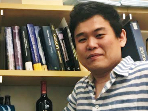
A KAIST alumnus and an associate professor at New York University (NYU), Dr. Kyunghyun Cho donated 3,000 USD to the KAIST Graduate School of AI to support female AI researchers.
Professor Cho spoke as a guest lecturer at the 2019 Samsung AI Forum on November 4 and received 3,000 USD as an honorarium. He donated this honorarium to the KAIST Graduate School of AI with a special request to support the school’s female PhD students attending the 2020 International Conference on Learning Representations (ICLR), where he serves as a program co-chair.
Professor Cho received his BS degree from KAIST’s School of Computing in 2009 and is now serving as an associate professor at NYU’s Computer Science Department and Center for Data Science. His research mainly covers machine learning and natural language processing.
Professor Cho said that he decided to make this donation because “In Korea and even in the US, women in science, technology, engineering, and mathematics (STEM) lack opportunities and environments that allow them to excel.”
Professor Song Chong, the Head of the KAIST Graduate School of AI, responded, “We are so grateful for Professor Kyunghyun Cho’s contribution and we will also use funds from the school in addition to the donation to support our female PhD students who will attend the ICLR.”
(END)
2019.11.15 View 9887
 -
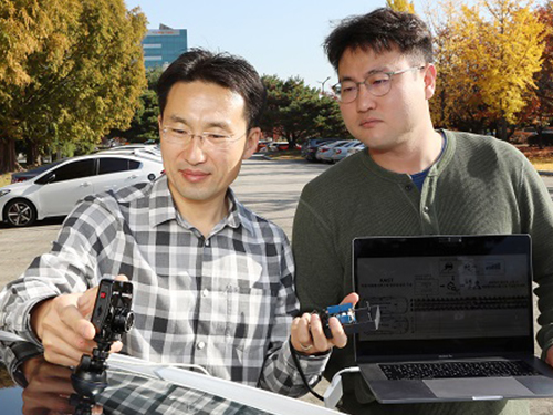 AI to Determine When to Intervene with Your Driving
(Professor Uichin Lee (left) and PhD candidate Auk Kim)
Can your AI agent judge when to talk to you while you are driving? According to a KAIST research team, their in-vehicle conservation service technology will judge when it is appropriate to contact you to ensure your safety.
Professor Uichin Lee from the Department of Industrial and Systems Engineering at KAIST and his research team have developed AI technology that automatically detects safe moments for AI agents to provide conversation services to drivers.
Their research focuses on solving the potential problems of distraction created by in-vehicle conversation services. If an AI agent talks to a driver at an inopportune moment, such as while making a turn, a car accident will be more likely to occur.
In-vehicle conversation services need to be convenient as well as safe. However, the cognitive burden of multitasking negatively influences the quality of the service. Users tend to be more distracted during certain traffic conditions. To address this long-standing challenge of the in-vehicle conversation services, the team introduced a composite cognitive model that considers both safe driving and auditory-verbal service performance and used a machine-learning model for all collected data.
The combination of these individual measures is able to determine the appropriate moments for conversation and most appropriate types of conversational services. For instance, in the case of delivering simple-context information, such as a weather forecast, driver safety alone would be the most appropriate consideration. Meanwhile, when delivering information that requires a driver response, such as a “Yes” or “No,” the combination of driver safety and auditory-verbal performance should be considered.
The research team developed a prototype of an in-vehicle conversation service based on a navigation app that can be used in real driving environments. The app was also connected to the vehicle to collect in-vehicle OBD-II/CAN data, such as the steering wheel angle and brake pedal position, and mobility and environmental data such as the distance between successive cars and traffic flow.
Using pseudo-conversation services, the research team collected a real-world driving dataset consisting of 1,388 interactions and sensor data from 29 drivers who interacted with AI conversational agents. Machine learning analysis based on the dataset demonstrated that the opportune moments for driver interruption could be correctly inferred with 87% accuracy.
The safety enhancement technology developed by the team is expected to minimize driver distractions caused by in-vehicle conversation services. This technology can be directly applied to current in-vehicle systems that provide conversation services. It can also be extended and applied to the real-time detection of driver distraction problems caused by the use of a smartphone while driving.
Professor Lee said, “In the near future, cars will proactively deliver various in-vehicle conversation services. This technology will certainly help vehicles interact with their drivers safely as it can fairly accurately determine when to provide conversation services using only basic sensor data generated by cars.”
The researchers presented their findings at the ACM International Joint Conference on Pervasive and Ubiquitous Computing (Ubicomp’19) in London, UK. This research was supported in part by Hyundai NGV and by the Next-Generation Information Computing Development Program through the National Research Foundation of Korea (NRF) funded by the Ministry of Science and ICT.
(Figure: Visual description of safe enhancement technology for in-vehicle conversation services)
2019.11.13 View 18741
 -
 Tungsten Suboxide Improves the Efficiency of Platinum in Hydrogen Production
< PhD Candidate Jinkyu Park and Professor Jinwoo Lee >
Researchers presented a new strategy for enhancing catalytic activity using tungsten suboxide as a single-atom catalyst (SAC). This strategy, which significantly improves hydrogen evolution reaction (HER) in metal platinum (pt) by 16.3 times, sheds light on the development of new electrochemical catalyst technologies.
Hydrogen has been touted as a promising alternative to fossil fuels. However, most of the conventional industrial hydrogen production methods come with environmental issues, releasing significant amounts of carbon dioxide and greenhouse gases.
Electrochemical water splitting is considered a potential approach for clean hydrogen production. Pt is one of the most commonly used catalysts to improve HER performance in electrochemical water splitting, but the high cost and scarcity of Pt remain key obstacles to mass commercial applications.
SACs, where all metal species are individually dispersed on a desired support material, have been identified as one way to reduce the amount of Pt usage, as they offer the maximum number of surface exposed Pt atoms.
Inspired by earlier studies, which mainly focused on SACs supported by carbon-based materials, a KAIST research team led by Professor Jinwoo Lee from the Department of Chemical and Biomolecular Engineering investigated the influence of support materials on the performance of SACs.
Professor Lee and his researchers suggested mesoporous tungsten suboxide as a new support material for atomically dispersed Pt, as this was expected to provide high electronic conductivity and have a synergetic effect with Pt.
They compared the performance of single-atom Pt supported by carbon and tungsten suboxide respectively. The results revealed that the support effect occurred with tungsten suboxide, in which the mass activity of a single-atom Pt supported by tungsten suboxide was 2.1 times greater than that of single-atom Pt supported by carbon, and 16.3 times higher than that of Pt nanoparticles supported by carbon.
The team indicated a change in the electronic structure of Pt via charge transfer from tungsten suboxide to Pt. This phenomenon was reported as a result of strong metal-support interaction between Pt and tungsten suboxide.
HER performance can be improved not only by changing the electronic structure of the supported metal, but also by inducing another support effect, the spillover effect, the research group reported. Hydrogen spillover is a phenomenon where adsorbed hydrogen migrates from one surface to another, and it occurs more easily as the Pt size becomes smaller.
The researchers compared the performance of single-atom Pt and Pt nanoparticles supported by tungsten suboxide. The single-atom Pt supported by tungsten suboxide exhibited a higher degree of hydrogen spillover phenomenon, which enhanced the Pt mass activity for hydrogen evolution up to 10.7 times compared to Pt nanoparticles supported by tungsten suboxide.
Professor Lee said, “Choosing the right support material is important for improving electrocatalysis in hydrogen production. The tungsten suboxide catalyst we used to support Pt in our study implies that interactions between the well-matched metal and support can drastically enhance the efficiency of the process.”
This research was supported by the Ministry of Science and ICT and introduced in the International Edition of the German journal Angewandte Chemie.
Figure. Schematic representation of hydrogen evolution reaction (HER) of pseudo single-atom Pt supported by tungsten suboxide
-Publication
Jinkyu Park, Dr. Seonggyu Lee, Hee-Eun Kim, Ara Cho, Seongbeen Kim, Dr. Youngjin Ye, Prof. Jeong Woo Han, Prof. Hyunjoo Lee, Dr. Jong Hyun Jang, and Prof. Jinwoo Lee. 2019. Investigation of the Support Effect in Atomically Dispersed Pt on WO3−x for Utilization of Pt in the Hydrogen Evolution Reaction. International Edition of Angewandte Chemie. Volume No. 58. Issue No. 45. 6 pages. https://doi.org/10.1002/anie.201908122
-ProfileProfessor Jinwoo LeeConvergence of Energy and Nano Science Laboratoryhttp://cens.kaist.ac.kr
Department of Chemical and Biomolecular EngineeringKAIST
2019.10.28 View 22240
 -
 A Single, Master Switch for Sugar Levels?
When a fly eats sugar, a single brain cell sends simultaneous messages to stimulate one hormone and inhibit another to control glucose levels in the body. Further research into this control system with remarkable precision could shed light on the neural mechanisms of diabetes and obesity in humans .
A single neuron appears to monitor and control sugar levels in the fly body, according to research published this week in Nature. This new insight into the mechanisms in the fly brain that maintain a balance of two key hormones controlling glucose levels, insulin and glucagon, can provide a framework for understanding diabetes and obesity in humans.
Neurons that sense and respond to glucose were identified more than 50 years ago, but what they do in our body has remained unclear. Researchers at the Korea Advanced Institute of Science and Technology (KAIST) and New York University School of Medicine have now found a single “glucose-sensing neuron” that appears to be the master controller in Drosophila, the vinegar fly, for maintaining an ideal glucose balance, called homeostasis.
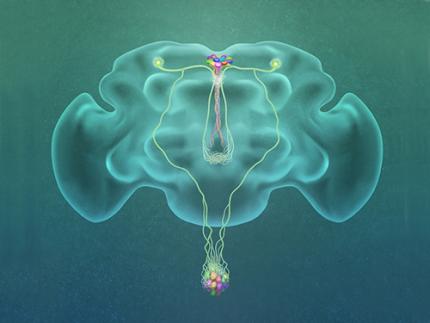
Professor Greg Seong-Bae Suh, Dr. Yangkyun Oh and colleagues identified a key neuron that is excited by glucose, which they called CN neuron. This CN neuron has a unique shape – it has an axon (which is used to transmit information to downstream cells) that is bifurcated. One branch projects to insulin-producing cells, and sends a signal triggering the secretion of the insulin equivalent in flies. The other branch projects to glucagon-producing cells and sends a signal inhibiting the secretion of the glucagon equivalent.
When flies consume food, the levels of glucose in their body increase; this excites the CN neuron, which fires the simultaneous signals to stimulate insulin and inhibit glucagon secretion, thereby maintaining the appropriate balance between the hormones and sugar in the blood. The researchers were able to see this happening in the brain in real time by using a combination of cutting-edge fluorescent calcium imaging technology, as well as measuring hormone and sugar levels and applying highly sophisticated molecular genetic techniques.
When flies were not fed, however, the researchers observed a reduction in the activity of CN neuron, a reduction in insulin secretion and an increase in glucagon secretion. These findings indicate that these key hormones are under the direct control of the glucose-sensing neuron. Furthermore, when they silenced the CN neuron rendering dysfunctional CN neuron in flies, these animals experienced an imbalance, resulting in hyperglycemia – high levels of sugars in the blood, similar to what is observed in diabetes in humans. This further suggests that the CN neuron is critical to maintaining glucose homeostasis in animals.
While further research is required to investigate this process in humans, Suh notes this is a significant step forward in the fields of both neurobiology and endocrinology.
“This work lays the foundation for translational research to better understand how this delicate regulatory process is affected by diabetes, obesity, excessive nutrition and diets high in sugar,” Suh said.
Profile: Greg Seong-Bae Suh
seongbaesuh@kaist.ac.kr
Professor Department of Biological Sciences
KAIST
(Figure: A single glucose-excited CN neuron extends bifurcated axonal branches,
one of which innervates insulin producing cells and stimulates their activity an the other axonal branch projects to glucagon producing cells and inhibits their activity.)
2019.10.24 View 18301
 -
 Two Professors Recognized for the National R&D Excellence 100
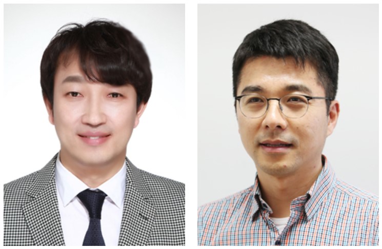
< Professor Haeng-Ki Lee (left) and Professor Jeong-Ho Lee (right) >
Two KAIST professors were listed among the 2019 National R&D Excellence 100 announced by the Ministry of Science and ICT and the Korea Institute of S&T Evaluation and Planning.
Professor Haeng-Ki Lee from the Department of Civil and Environmental Engineering was recognized in the field of mechanics and materials for his research on developing new construction materials through the convergence of nano- and biotechnologies.
In the field of life and marine science, Professor Jeong-Ho Lee from the Graduate School of Medical Science and Engineering was lauded for his research of diagnostic tools and therapies for glioblastoma and pediatric brain tumors.
A certificate from the Minister of Ministry of Science and ICT will be conferred to these two professors, and their names will be inscribed on a special 2019 National R&D Excellence 100 plaque to celebrate their achievements. The professors will also be given privileges during the process of new R&D project selection.
(END)
2019.10.15 View 13067
 -
 Professor Byong-Guk Park Named Scientist of October
< Professor Byong-Guk Park >
Professor Byong-Guk Park from the Department of Materials Science and Engineering was selected as the ‘Scientist of the Month’ for October 2019 by the Ministry of Science and ICT and the National Research Foundation of Korea. Professor Park was recognized for his contributions to the advancement of spin-orbit torque (SOT)-based magnetic random access memory (MRAM) technology. He received 10 million KRW in prize money.
A next-generation, non-volatile memory device MRAM consists of thin magnetic films. It can be applied in “logic-in-memory” devices, in which logic and memory functionalities coexist, thus drastically improving the performance of complementary metal-oxide semiconductor (CMOS) processors. Conventional MRAM technology is limited in its ability to increase the operation speed of a memory device while maintaining a high density.
Professor Park tackled this challenge by introducing a new material, antiferromagnet (IrMn), that generates a sizable amount of SOT as well as an exchange-bias field, which makes successful data writing possible without an external magnetic field. This research outcome paved the way for the development of MRAM, which has a simple device structure but features high speeds and density.
Professor Park said, “I feel rewarded to have forwarded the feasibility and applicability of MRAM. I will continue devoting myself to studying further on the development of new materials that can help enhance the performance of memory devices."
(END)
2019.10.10 View 10975
 -
 Object Identification and Interaction with a Smartphone Knock
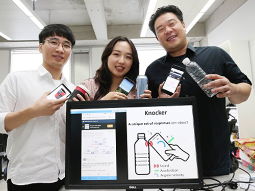
(Professor Lee (far right) demonstrate 'Knocker' with his students.)
A KAIST team has featured a new technology, “Knocker”, which identifies objects and executes actions just by knocking on it with the smartphone. Software powered by machine learning of sounds, vibrations, and other reactions will perform the users’ directions.
What separates Knocker from existing technology is the sensor fusion of sound and motion. Previously, object identification used either computer vision technology with cameras or hardware such as RFID (Radio Frequency Identification) tags. These solutions all have their limitations. For computer vision technology, users need to take pictures of every item. Even worse, the technology will not work well in poor lighting situations. Using hardware leads to additional costs and labor burdens.
Knocker, on the other hand, can identify objects even in dark environments only with a smartphone, without requiring any specialized hardware or using a camera. Knocker utilizes the smartphone’s built-in sensors such as a microphone, an accelerometer, and a gyroscope to capture a unique set of responses generated when a smartphone is knocked against an object. Machine learning is used to analyze these responses and classify and identify objects.
The research team under Professor Sung-Ju Lee from the School of Computing confirmed the applicability of Knocker technology using 23 everyday objects such as books, laptop computers, water bottles, and bicycles. In noisy environments such as a busy café or on the side of a road, it achieved 83% identification accuracy. In a quiet indoor environment, the accuracy rose to 98%.
The team believes Knocker will open a new paradigm of object interaction. For instance, by knocking on an empty water bottle, a smartphone can automatically order new water bottles from a merchant app. When integrated with IoT devices, knocking on a bed’s headboard before going to sleep could turn off the lights and set an alarm. The team suggested and implemented 15 application cases in the paper, presented during the 2019 ACM International Joint Conference on Pervasive and Ubiquitous Computing (UbiComp 2019) held in London last month.
Professor Sung-Ju Lee said, “This new technology does not require any specialized sensor or hardware. It simply uses the built-in sensors on smartphones and takes advantage of the power of machine learning. It’s a software solution that everyday smartphone users could immediately benefit from.” He continued, “This technology enables users to conveniently interact with their favorite objects.”
The research was supported in part by the Next-Generation Information Computing Development Program through the National Research Foundation of Korea funded by the Ministry of Science and ICT and an Institute for Information & Communications Technology Promotion (IITP) grant funded by the Ministry of Science and ICT.
Figure: An example knock on a bottle. Knocker identifies the object by analyzing a unique set of responses from the knock, and automatically launches a proper application or service.
2019.10.02 View 29115
 -
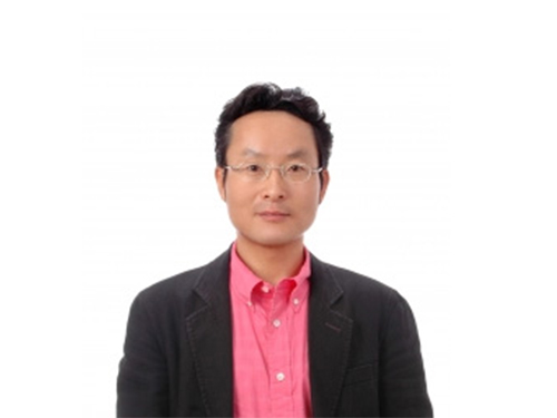 Professor Hyun Gyu Park Appointed as Associate Editor for Biosensors and Bioelectronics
Professor Hyun Gyu Park from the Department of Chemical and Biomolecular Engineering was appointed as an associate editor for Biosensors and Bioelectronics, an international journal published by Elsevier.
Biosensors and Bioelectronics is one of the top SCI journals in the fields of chemistry and analytical science (IF 9.518 as of 2018). Professor Park was recognized and appointed as the associate editor for this journal due to his outstanding research achievements in the fields of nucleic acid engineering, biosensors, and nanobiotechnology.
Professor Park will serve as the associate editor from this October until December 2021.
(END)
2019.10.01 View 8330
 -
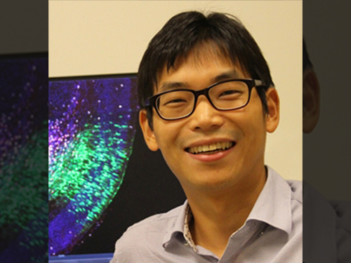 Professor Ki-Jun Yoon selected as the 2019 SUHF Young Investigator
< Professor Ki-Jun Yoon >
Professor Ki-Jun Yoon from the Department of Biological Sciences was named one of four recipients of the 2019 Suh Kyung-Bae Science Foundation (SUHF) Young Investigator Awards.
The SUHF is a non-profit organization established in 2016 and funded by a personal donation of 300 billion KRW in shares from Chairman and CEO Kyung-Bae Suh of the Amorepacific Group. The primary purpose of the foundation is to serve as a platform to nurture and provide comprehensive long-term support for creative and passionate young Korean scientists committed to pursuing research in the field of life sciences. The SUHF selects three to five scientists through an open recruiting process every year, and grants each scientist a maximum of 2.5 billion KRW over a period of up to five years.
Since January this year, the foundation received 83 research proposals from scientists across the nation, especially from those who had less than five years of experience as professors, and selected the four recipients, including Professor Yoon.
Professor Yoon was recognized for his contributions to the advancement of research on how post-transcriptional mechanisms may modulate stem cell properties. His research project involves deciphering the molecular mechanisms controlling RNA metabolism in neural stem cells during normal development, and how alterations in RNA regulatory programs lead to human brain disorders.
< (From left) Professor Joo-Hong Park, Professor Yuree Lee, Chairman and CEO Kyung-Bae Suh, Professor Eunjung Lee, Professor Ki-Jun Yoon, ⓒ Amorepacific Group >
The other awards were given to Professor Joo-Hong Park and Professor Yuree Lee of Seoul National University, and Professor Eunjung Lee of Boston Children's Hospital and Harvard Medical School.
The awards ceremony was held on September 18 at the Amorepacific Headquarters in Seoul.
With these four new awardees, a total of 14 scientists have been named as SUHF Young Investigators to date.
(END)
2019.09.23 View 9775