Quantum
-
 Improved Efficiency of CQD Solar Cells Using an Organic Thin Film
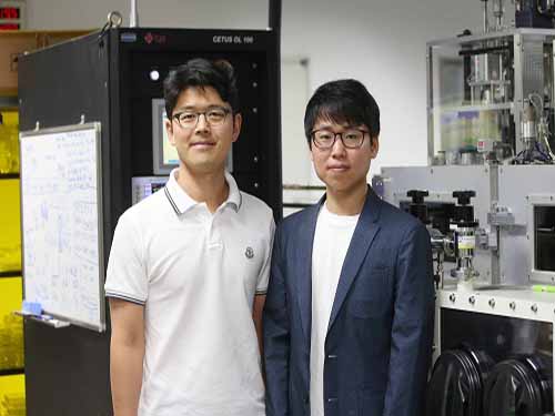
(from left: Professor Jung-Yong Lee and Dr. Se-Woong Baek)
Recently, the power conversion efficiency (PCE) of colloidal quantum dot (CQD)-based solar cells has been enhanced, paving the way for their commercialization in various fields; nevertheless, they are still a long way from being commercialized due to their efficiency not matching their stability. In this research, a KAIST team achieved highly stable and efficient CQD-based solar cells by using an amorphous organic layer to block oxygen and water permeation.
CQD-based solar cells are light-weight, flexible, and they boost light harvesting by absorbing near-infrared lights. Especially, they draw special attention for their optical properties controlled efficiently by changing the quantum dot sizes. However, they are still incompatible with existing solar cells in terms of efficiency, stability, and cost. Therefore, there is great demand for a novel technology that can simultaneously improve both PCE and stability while using an inexpensive electrode material.
Responding to this demand, Professor Jung-Yong Lee from the Graduate School of Energy, Environment, Water and Sustainability and his team introduced a technology to improve the efficiency and stability of CQD-based solar cells.
The team found that an amorphous organic thin film has a strong resistance to oxygen and water. Using these properties, they employed this doped organic layer as a top-hole selective layer (HSL) for the PbS CQD solar cells, and confirmed that the hydro/oxo-phobic properties of the layer efficiently protected the PbS layer. According to the molecular dynamics simulations, the layer significantly postponed the oxygen and water permeation into the PbS layer. Moreover, the efficient injection of the holes in the layer reduced interfacial resistance and improved performance.
With this technology, the team finally developed CQD-based solar cells with excellent stability. The PCE of their device stood at 11.7% and maintained over 90% of its initial performance when stored for one year under ambient conditions.
Professor Lee said, “This technology can be also applied to QD LEDs and Perovskite devices. I hope this technology can hasten the commercialization of CQD-based solar cells.”
This research, led by Dr. Se-Woong Baek and a Ph.D. student, Sang-Hoon Lee, was published in Energy & Environmental Science on May 10.
Figure 1. The schematic of the equilibrated structure of the amorphous organic film
Figure 2. Schematic illustration of CQD-based solar cells and graphs showing their performance
2018.08.27 View 9305
 -
 Three Professors Named KAST Fellows
(Professor Dan Keun Sung at the center)
(Professor Y.H. Cho at the center)
(Professor K.H. Cho at the center)
The Korean Academy of Science and Technology (KAST) inducted three KAIST professors as fellows at the New Year’s ceremony held at KAST on January 12. They were among the 24 newly elected fellows of the most distinguished academy in Korea. The new fellows are Professor Dan Keun Sung of the School of Electrical Engineering, Professor Kwang-Hyun Cho of the Department of Bio and Brain Engineering, and Professor Yong-Hoon Cho of the Department of Physics.
Professor Sung was recognized for his lifetime academic achievements in fields related with network protocols and energy ICT. He also played a crucial role in launching the Korean satellites KITSAT-1,2,3 and the establishment of the Satellite Technology Research Center at KAIST.
Professor Y.H.Cho has been a pioneer in the field of low-dimensional semiconductor-powered quantum photonics that enables quantum optical research in solid state. He has been recognized as a renowned scholar in this field internationally.
Professor K.H.Cho has conducted original research that combines IT and BT in systems biology and has applied novel technologies of electronic modeling and computer simulation analysis for investigating complex life sciences. Professor Cho, who is in his 40s, is the youngest fellow among the newly inducted fellows.
2018.01.16 View 17222
 -
 ANSYS Korea Donates Engineering Simulation Software
ANSYS Korea made an in-kind donation of engineering simulation software, Multiphysics Campus Solution, to KAIST on March 24. ANSYS Korea donated 10,000 copies for education and 1,000 copies for research valued at about 4 billion KRW (about 200 billion KRW commercially).
The ANSYS software will benefit the engineering simulation work in nine departments and 60 labs for three years, including the departments of mechanical engineering, aerospace engineering, electrical engineering, civil and environmental engineering, nuclear and quantum engineering, chemical and bimolecular engineering, bio and brain engineering, materials science and engineering, and the Cho Chun Shik Graduate School of Green Transportation.
ANSYS is a global engineering simulation company. It provides ANSYS CAE (Computer Aided Engineering) software products in various industries in the world as well as various support, training, and consulting services. Deemed an exemplary model of university-industry R&D collaboration especially in the Industry 4.0 era, their donation will help create the best engineering education environment possible at KAIST.
ANSYS's multi-physics campus solution is a comprehensive software suite that spans the entire range of physics, providing access to virtually any field of engineering simulation that a design process requires. It expands the fields of fluids, structures, electromagnetics, and semiconductors. Undergraduates use it to learn physics principles and gain hands-on, real-world experience that can lead to a deeper understanding of engineering concepts. Postgraduate researchers apply simulation tools to solve complex engineering problems and produce data for their theses.
"Engineering simulations are playing a stronger role in science and engineering. ANSYS software will help our undergraduates and our researchers learn the principles of physics and deepen their understanding of engineering concepts. We hope this will serve as an instrumental tool for multidisciplinary studies, critical to fostering our students," said President Sung-Chul Shin.
ANSYS Korea CEO Yong-Won Cho added, "We sincerely hope our software will help KAIST students and researchers experience the best engineering education and achieve significant research results."
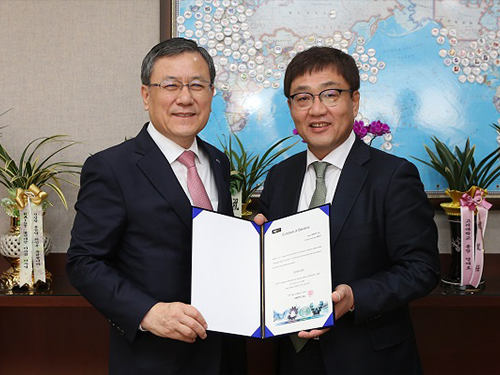
(Photo caption: President Shin (left) poses with ANSYS Korea CEO Yong-Won Cho at the donation ceremony on March 24 at KAIST)
2017.03.24 View 10692
 -
 News Article on the Development of Synthesis Process for Graphene Quantum Dots
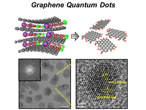
Before It's News, an international online news agency, highlighted the recent research conducted by KAIST professors (Seokwoo Jeon of the Department of Materials Science and Engineering, Yong-Hoon Cho of the Department of Physics, and Seunghyup Yoo of the Department of Electrical Engineering) on the development of synthesis process for graphene quantum dots, nanometer-sized round semiconductor nanoparticles that are very efficient at emitting photons. If commercialized, this synthetic technology will lead the way to the development of paper-thin displays in the future.
For the article, please go to the link below:
Before It’s News, September 3, 2014“Graphene quantum dots prove highly efficient in emitting light”
http://beforeitsnews.com/science-and-technology/2014/09/graphene-quantum-dots-prove-highly-efficient-in-emitting-light-2718190.html
2014.09.07 View 16108
 -
 Extracting Light from Graphite: Core Technology of Graphene Quantum Dots Display Developed
Professor Seokwoo Jeon of the Department of Materials Science and Engineering, Professor Yong-Hoon Cho of the Department of Physics, and Professor Seunghyup Yoo of the Department of Electrical Engineering announced that they were able to develop topnotch graphene quantum dots from graphite.
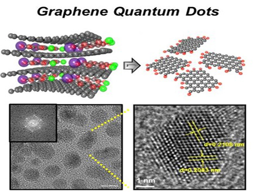
Using the method of synthesizing graphite intercalation compound from graphite with salt and water, the research team developed graphene quantum dots in an ecofriendly way.
The quantum dots have a diameter of 5 nanometers with their sizes equal and yield high quantum efficiency. Unlike conventional quantum dots, they are not comprised of toxic materials such as lead or cadmium. As the quantum dots can be developed from materials which can be easily found in the nature, researchers look forward to putting these into mass production at low cost.
The research team also discovered a luminescence mechanism of graphene quantum dots and confirmed the possibility of commercial use by developing quantum dot light-emitting diodes with brightness of 1,000 cd/m2, which is greater than that of cellphone displays.
Professor Seokwoo Jeon said, “Although quantum dot LEDs have a lower luminous efficiency than existing ones, their luminescent property can be further improved” and emphasized that “using quantum dot displays will allow us to develop not only paper-thin displays but also flexible ones.”
Sponsored by Graphene Research Center in KAIST Institute for NanoCentury, the research finding was published online in the April 20th issue of Advanced Optical Materials.
Picture 1: Graphene quantum dots and their synthesis
Picture 2: Luminescence mechanism of graphene quantum dots
Picture 3: Structure of graphene quantum dots LED and its emission
2014.09.06 View 20721
 -
 2014 NEREC Conference on Nuclear Nonproliferation: July 31-August 1, 2014, Seoul
The Nonproliferation Education and Research Center (NEREC) at KAIST hosted an international conference on nuclear nonproliferation on July 31-August 1, 2014 in Seoul. The Ministry of Science, ICT and Future Planning, the Korean Nuclear Safety and Security Commission, and the Korea Nuclear Policy Society (KNPS) sponsored the event.
Over one hundred experts and "thought leaders" in nuclear security and nonproliferation attended the conference and discussed issues related to the nonproliferation of nuclear weapons, the role of scientific community in mitigating nuclear threat and promoting the peaceful use of nuclear power, and nuclear disarmament policy.
Keynote speakers were: Steven E. Miller, Director of International Security Program at Belfer Center for Science and International Affairs, Harvard University; Scott D. Sagan, Senior Fellow of the Center for International Security and Cooperation, Freeman Spogli Institute for International Studies, Stanford University; Mark Fitzpatrick, Director of the Nonproliferation and Disarmament Programme, International Institute for Strategic Studies; Sang-Hyun Lee, Director of Security Strategy, Sejong Institute; and Man-Sung Yim, Professor of Nuclear and Quantum Engineering, KAIST.
At the conference, Professor Yim, Director of KAIST NEREC said, “Korea has grown to become a key player in the development of commercial nuclear energy over the past decades. We hope that our conference encourages Korea to be more involved in the efforts of the international community to enhance the global nonproliferation regime.”
2014.08.05 View 16847
 -
 Short Wavelength, Ultra-High Speed Quantum Light Source based on Quantum Dot Developed
Professor Yong Hoon, Cho (Department of Physics) and his research team synthesized an obelisk nanostructure and successfully formed a single semiconductor quantum exhibiting high reliability to realize an ultra-high speed, highly efficient, release of quantum dots.
The result of the research effort was published in the July 5th online edition of Scientific Reports published by Nature.
Semiconductor Quantum Dots restrict electrons within a cubic boundary of few nanometers thereby exhibiting similar properties to an atom with discontinuous energy levels. Exploitation of this characteristic makes possible the development of quantum light source, critical for next generation quantum information communication and quantum encryption.
High operational temperatures, stability, rapid photon release, electric current capability, and other advantages are reasons why semiconductor quantum dots are regarded as next generation core technology.
However conventional, spontaneously formed quantum dots are densely packed in a planar structure rendering the analysis of a single quantum dot difficult and result in the poor efficiency of photon release. In addition, the internal electromagnetic effect which is caused by inter-planar stress results in low internal quantum efficiency due to the difficulty in electron-hole recombination.
Professor Cho’s research team synthesized an obelisk shaped nanostructure using nitrides that emit short wavelengths of light. The activation layer was grown on the tip of the nanostructure and the team succeeded in placing a single quantum dot on the nano-tip. The team was therefore able to confirm the ultra-high speed single photon characteristics which occur at low energy levels.
Use of unique nanostructures makes synthesis of single atomic structures without processes like patterning while enabling the release of light emitted by the quantum dot.
Using this unique method the team showed the increase in internal quantum efficiency. The electromagnetic forces apparent in thin films no longer affects the quantum dot greatly due to the obelisk structure’s reduced inter planar stress.
The newly developed quantum light source emits visible light (400nm range) and not the conventional infrared light. This characteristic makes possible it use in communication in free space and enables use of highly efficient, visible range photon detector.
Professor Cho commented that “the developed method makes quantum dot growth much easier making single photon synthesis much faster to contribute to the development of practical quantum light source.” And that “the characteristics of the obelisk nanostructure enable the easy detachment from and attachment to other substrates enabling its use in producing single chip quantum light source.”
The research was conducted under the supervision of Professor Cho. The researchers werey Jae Hyung, Kim (first author) and Yong Ho, Ko (second author), both Ph.D. candidates at KAIST. The Ministry of Science, ICT and Future Planning, the National Research Foundation, and WCU Program provided support to the research effort.
2013.08.23 View 9727
 -
 Dopant properties of silicon nanowires investigated
Professor Chang Kee Joo
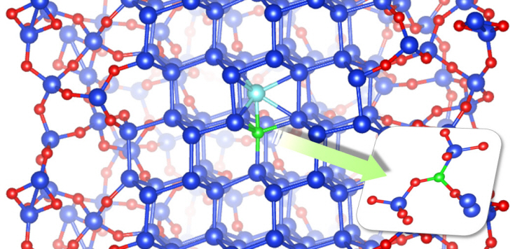
Professor Kee Joo Chang’s research team from the Department of Physics at KAIST has successfully unearthed the properties of boron and phosphorous dopants in silicon nanowires, a material expected to be used in next generation semiconductors. The research team was the first in the world to investigate the movement of boron and phosphorous (impurities or ‘dopants’ added for electrical flow) in oxidized silicon nanowires and study the mechanism behind its deactivation.
It is nearly impossible to develop a silicon based semiconductor thinner than 10nm, even using the most advanced modern technology. However, the thickness of silicon nanowires are within the nano level and hence, allows a higher degree of integration in semiconductors.
For silicon nanowires to carry electricity, small amounts of boron and phosphorous need to be added (‘doping’ process). Compared to silicon, nanowires are harder to create due to the difficulties in the doping process as well as the control of electrical conduction properties.
Professor Chang’s research team improved upon the existing simple model by applying revolutionary quantum simulation theory to create a realistic core-shell atomic model. This research successfully investigated the cause of the escape of boron dopants from the silicon core during oxidation. It was also found that although phosphorous dopants do not escape as oxides, they form electrically deactivated pairs which decreases the efficiency. These phenomena were attributed to the film shape of the nano-wires, which increases the relative surface area compared to a same volume of silicon.
The research results were published in the online September edition of the world renowned Nano Letters.
Figure: The longitudinal section diagram of the Silicon/oxide core-shell model
2012.11.28 View 9465
 -
 KAIST researchers verify and control the mechanical properties of graphene
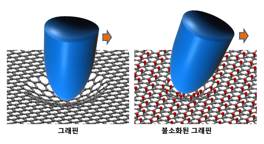
KAIST researchers have successfully verified and controlled the mechanical properties of graphene, a next-generation material. Professor Park Jung Yong from the EEWS Graduate School and Professor Kim Yong Hyun from the Graduate School of Nanoscience and Technology have succeeded in fluorinating a single atomic-layered graphene sample and controlling its frictional and adhesive properties. This is the first time the frictional properties of graphene have been examined at the atomic level, and the technology is expected to be applied to nano-sized robots and microscopic joints.
Graphene is often dubbed “the dream material” because of its ability to conduct high amounts of electricity even when bent, making it the next-generation substitute for silicon semiconductors, paving the way for flexible display and wearable computer technologies. Graphene also has high potential applications in mechanical engineering because of its great material strength, but its mechanical properties remained elusive until now.
Professor Park’s research team successfully produced individual graphene samples with fluorine-deficiency at the atomic level by placing the samples in Fluoro-xenon (XeF2) gas and applying heat. The surface of the graphene was scanned using a micro probe and a high vacuum atomic microscope to measure its dynamic properties.
The research team found that the fluorinated graphene sample had 6 times more friction and 0.7 times more adhesiveness than the original graphene. Electrical measurements confirmed the fluorination process, and the analysis of the findings helped setup the theory of frictional changes in graphene.
Professor Park stated that “graphene can be used for the lubrication of joints in nano-sized devices” and that this research has numerous applications such as the coating of graphene-based microdynamic devices.
This research was published in the online June edition of Nano Letters and was supported by the Ministry of Science, Technology, and Education and the National Research Foundation as part of the World Class University (WCU) program.
2012.07.24 View 19078