Department+of+Chemistry
-
 Development of Gold Nanowire Probe Needle with an Increased Sensitivity
Professor Bongsoo Kim
The newly developed nano-probe needle’s thickness estimates only at 0.1 micrometers with an increased 1,000-fold sensitivity and spatial resolution of 1mm.
Professor Bongsoo Kim and his research team from the Department of Chemistry, KASIT, including the first author, Dr. Mijeong Kang, succeeded in measuring nerve signals of a mouse using the world’s thinnest nano-probe needle made of single-crystal gold nanowires.
The newly developed nano-probe needle possesses the thickness of 100 nanometers (nm), which shows 1,000 times more sensitivity than the conventional nerve probe needles, as well as accurately measures nerve signals with an extremely fine resolution of less than 1mm. Unlike the existing probe needles that cause neural tissues to be damaged during insertion, the new nano-probe needle minimizes the damage and thus can detect large nerve signals.
The brain neural probe, which collects and analyzes electrical nerve signals generated in the brain, is the most essential element in brain research. A neural probe should minimize tissue damages, but needs to possess a good electrical sensitivity.
The researchers first applied heat on the gold, which is the necessary material for a probe, until it turned to a vapor phase. Then, the gold evaporation slug was transported to a colder board and left to form single-crystal gold nano structures by condensation. Because the new gold nanowire, produced by using this principle, is a flawless single crystal structure, it shows strong and flexible properties.
Professor Kim and his team applied the nano-probe needle into the brain of a mouse that has been administered a drug to induce epilepsy. They were able to find the exact area in the brain that triggers epilepsy. Furthermore, the researchers also detected neural signal changes in the brain of the mouse when it encountered the intrusion of a stranger mouse.
Professor Bongsoo Kim commented the meaning of his research:
“The new nano-probe needle is able to detect signals from a single nerve cell with high sensitivity while preserving the nerve cells intact. The probe needle will be useful for creating a precise three-dimensional brain map, as well as providing electrical treatment for brain diseases such as dementia and Parkinson's disease.”
This research results were published online in the August 12, 2014 edition of ACS Nano.
2014.09.06 View 7347
Development of Gold Nanowire Probe Needle with an Increased Sensitivity
Professor Bongsoo Kim
The newly developed nano-probe needle’s thickness estimates only at 0.1 micrometers with an increased 1,000-fold sensitivity and spatial resolution of 1mm.
Professor Bongsoo Kim and his research team from the Department of Chemistry, KASIT, including the first author, Dr. Mijeong Kang, succeeded in measuring nerve signals of a mouse using the world’s thinnest nano-probe needle made of single-crystal gold nanowires.
The newly developed nano-probe needle possesses the thickness of 100 nanometers (nm), which shows 1,000 times more sensitivity than the conventional nerve probe needles, as well as accurately measures nerve signals with an extremely fine resolution of less than 1mm. Unlike the existing probe needles that cause neural tissues to be damaged during insertion, the new nano-probe needle minimizes the damage and thus can detect large nerve signals.
The brain neural probe, which collects and analyzes electrical nerve signals generated in the brain, is the most essential element in brain research. A neural probe should minimize tissue damages, but needs to possess a good electrical sensitivity.
The researchers first applied heat on the gold, which is the necessary material for a probe, until it turned to a vapor phase. Then, the gold evaporation slug was transported to a colder board and left to form single-crystal gold nano structures by condensation. Because the new gold nanowire, produced by using this principle, is a flawless single crystal structure, it shows strong and flexible properties.
Professor Kim and his team applied the nano-probe needle into the brain of a mouse that has been administered a drug to induce epilepsy. They were able to find the exact area in the brain that triggers epilepsy. Furthermore, the researchers also detected neural signal changes in the brain of the mouse when it encountered the intrusion of a stranger mouse.
Professor Bongsoo Kim commented the meaning of his research:
“The new nano-probe needle is able to detect signals from a single nerve cell with high sensitivity while preserving the nerve cells intact. The probe needle will be useful for creating a precise three-dimensional brain map, as well as providing electrical treatment for brain diseases such as dementia and Parkinson's disease.”
This research results were published online in the August 12, 2014 edition of ACS Nano.
2014.09.06 View 7347 -
 Review of organophosphonate nerve agent remediation and sensing chemistry
Professor David Churchill, Dept. of Chemistry, KAIST
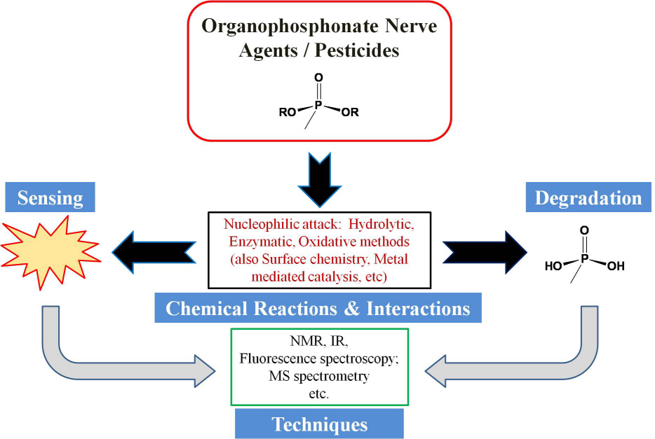
Scientists in Daejeon, South Korea and Lexington, Kentucky (USA) have recently published a review on the subject of nerve agent remediation and probing chemistry (Chemical Reviews, DOI:10.1021/cr100193y). This article endeavored to pursue organophosphonate nerve agent chemistry deeply and comprehensively and to reflect that decontamination / sensing and nerve agents / pesticides are quite inextricable: when one tries to degrade nerve agents one also needs to detect what components are still present “downstream,” etc. Nerve agents and many pesticides also share a common generalized organophosphate / -phosphonate structure.
Also, the use of simulant molecules (mimics) and a consideration of the closely related organophosphonate pesticides were also treated comprehensively in the Review. The authors reached back into the literature when developing some sections to make important connections to the contemporary topics of interest. The review also includes industrial insights.
Kibong Kim, Olga G. Tsay and David G. Churchill of the Department of Chemistry at KAIST and David A. Atwood of the Department of Chemistry of the University of Kentucky endeavored to "make a variety of connections in research strategies and (sub-) fields to present what is still possible, fruitful, practical, and necessary and to facilitate a current comprehensive molecular level understanding of organophosphonate degradation and sensing," Churchill says.
The authors feel that for the time being, researchers in varying research areas “can use this manuscript effectively when considering future research directions.”
2011.09.19 View 10402
Review of organophosphonate nerve agent remediation and sensing chemistry
Professor David Churchill, Dept. of Chemistry, KAIST
Scientists in Daejeon, South Korea and Lexington, Kentucky (USA) have recently published a review on the subject of nerve agent remediation and probing chemistry (Chemical Reviews, DOI:10.1021/cr100193y). This article endeavored to pursue organophosphonate nerve agent chemistry deeply and comprehensively and to reflect that decontamination / sensing and nerve agents / pesticides are quite inextricable: when one tries to degrade nerve agents one also needs to detect what components are still present “downstream,” etc. Nerve agents and many pesticides also share a common generalized organophosphate / -phosphonate structure.
Also, the use of simulant molecules (mimics) and a consideration of the closely related organophosphonate pesticides were also treated comprehensively in the Review. The authors reached back into the literature when developing some sections to make important connections to the contemporary topics of interest. The review also includes industrial insights.
Kibong Kim, Olga G. Tsay and David G. Churchill of the Department of Chemistry at KAIST and David A. Atwood of the Department of Chemistry of the University of Kentucky endeavored to "make a variety of connections in research strategies and (sub-) fields to present what is still possible, fruitful, practical, and necessary and to facilitate a current comprehensive molecular level understanding of organophosphonate degradation and sensing," Churchill says.
The authors feel that for the time being, researchers in varying research areas “can use this manuscript effectively when considering future research directions.”
2011.09.19 View 10402 -
 Spintronics: A high wire act by Nanowerk News
An article by Nanowerk News on the integration of ferromagnetic nanowire arrays on grapheme substrates was published. Professor Bong-Soo Kim from the Department of Chemistry, KAIST, led the research in conjunction with Hanyang University and Samsung in Korea.
http://www.nanowerk.com/news/newsid=22204.php
Posted: Jul 25th, 2011
Spintronics: A high wire act
(Nanowerk News) Graphene is a promising material for a wide range of applications due to its remarkable mechanical and electronic properties. An application of particular interest is spin-based electronics, or spintronics, in which the spin orientation of an electron is used to perform circuit functions in addition to its charge. Bongsoo Kim and colleagues from KAIST, Hanyang University and Samsung in Korea now report the integration of ferromagnetic nanowire arrays on graphene substrates, opening up a route for the construction of graphene-based spintronic devices using nanowires as spin-injecting contacts ("Epitaxially Integrating Ferromagnetic Fe1.3Ge Nanowire Arrays on Few-Layer Graphene").
The spin of an electron is a property that, like charge, can be used to encode, process and transport information. However, spin information is easily lost in most media, which has made spintronics difficult to realize in practice. In graphene, on the other hand, spin can be preserved for longer due to its peculiar electron transport properties. "Low intrinsic spin–orbit coupling, long spin diffusion lengths and vanishing hyperfine interaction are features of graphene that make it a promising medium for spin transport," explains Kim.
Scanning electron microscopy image of vertical iron germanide nanowires grown on graphene. (© ACS 2011)
A prerequisite for the realization of spintronic devices based on graphene is its integration with ferromagnetic contacts to allow spin injection. Kim and his co-workers found that nanowires of iron germanide (Fe1.3Ge) serve as efficient contacts for this purpose. "Iron germanide nanowires show low resistivity and room-temperature ferromagnetism, and they are compatible with existing complementary metal–oxide–semiconductor technologies," says Kim.
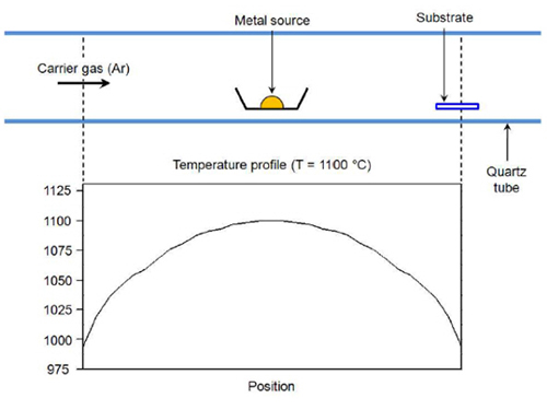
To produce the atomically well-defined interfacial contact between the nanowires and the graphene surface needed for optimum device performance, the researchers deposited the contacts by an epitaxial method based on chemical vapor transport. Through careful adjustment of deposition parameters such as carrier gas flow rate and reaction temperature, the researchers produced vertically aligned nanowires that are closely lattice-matched to the graphene sheets (see image).
Initially preparing the graphene sheets on a substrate of silicon oxide allowed the researchers to isolate the final nanowire–graphene structure by etching and then transfer it to another substrate, greatly expanding the versatility of the approach. It is a delicate process, however. "It is necessary to transfer the graphene films onto the substrate very carefully in order to avoid folding and wrinkling of the graphene," says Kim.
Source: Tokyo Institute of Technology
2011.07.26 View 12359
Spintronics: A high wire act by Nanowerk News
An article by Nanowerk News on the integration of ferromagnetic nanowire arrays on grapheme substrates was published. Professor Bong-Soo Kim from the Department of Chemistry, KAIST, led the research in conjunction with Hanyang University and Samsung in Korea.
http://www.nanowerk.com/news/newsid=22204.php
Posted: Jul 25th, 2011
Spintronics: A high wire act
(Nanowerk News) Graphene is a promising material for a wide range of applications due to its remarkable mechanical and electronic properties. An application of particular interest is spin-based electronics, or spintronics, in which the spin orientation of an electron is used to perform circuit functions in addition to its charge. Bongsoo Kim and colleagues from KAIST, Hanyang University and Samsung in Korea now report the integration of ferromagnetic nanowire arrays on graphene substrates, opening up a route for the construction of graphene-based spintronic devices using nanowires as spin-injecting contacts ("Epitaxially Integrating Ferromagnetic Fe1.3Ge Nanowire Arrays on Few-Layer Graphene").
The spin of an electron is a property that, like charge, can be used to encode, process and transport information. However, spin information is easily lost in most media, which has made spintronics difficult to realize in practice. In graphene, on the other hand, spin can be preserved for longer due to its peculiar electron transport properties. "Low intrinsic spin–orbit coupling, long spin diffusion lengths and vanishing hyperfine interaction are features of graphene that make it a promising medium for spin transport," explains Kim.
Scanning electron microscopy image of vertical iron germanide nanowires grown on graphene. (© ACS 2011)
A prerequisite for the realization of spintronic devices based on graphene is its integration with ferromagnetic contacts to allow spin injection. Kim and his co-workers found that nanowires of iron germanide (Fe1.3Ge) serve as efficient contacts for this purpose. "Iron germanide nanowires show low resistivity and room-temperature ferromagnetism, and they are compatible with existing complementary metal–oxide–semiconductor technologies," says Kim.
To produce the atomically well-defined interfacial contact between the nanowires and the graphene surface needed for optimum device performance, the researchers deposited the contacts by an epitaxial method based on chemical vapor transport. Through careful adjustment of deposition parameters such as carrier gas flow rate and reaction temperature, the researchers produced vertically aligned nanowires that are closely lattice-matched to the graphene sheets (see image).
Initially preparing the graphene sheets on a substrate of silicon oxide allowed the researchers to isolate the final nanowire–graphene structure by etching and then transfer it to another substrate, greatly expanding the versatility of the approach. It is a delicate process, however. "It is necessary to transfer the graphene films onto the substrate very carefully in order to avoid folding and wrinkling of the graphene," says Kim.
Source: Tokyo Institute of Technology
2011.07.26 View 12359