Wiley
-
 Computer Simulation Identifies a Key Principle for Next-generation Carbon Fibers
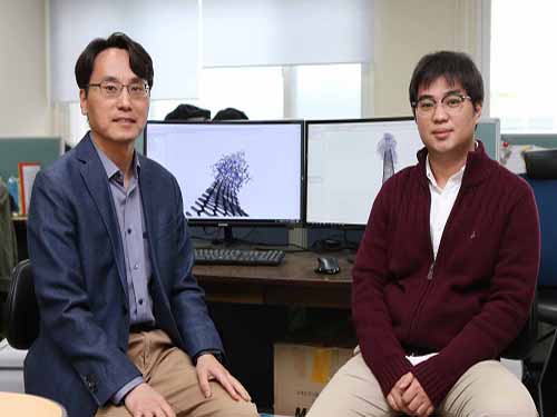
(from left: Professor Yong-Hoon Kim and PhD candidate Juho Lee)
Performing state-of-the-art computer simulations, a KAIST research team identified an atomistic design principle to produce high-quality, next-generation carbon fibers.
Carbon fibers are light-weight yet excellent in mechanical strength and thermal resistance. Boasting these properties, they can be diversely applied in high-technology sectors, including automotive, aerospace, and nuclear engineering.
They are produced from a polymer precursor through a series of spinning, stabilization, and carbonization processes. However, there is a major obstacle to producing high-quality carbon fibers. That is, when there exist ill-defined regions within the polymer matrixes, they result in disorder and defects within the produced carbon fibers.
As a solution to this problem, it was proposed that the introduction of carbon nanotubes (CNT) could enhance polymer orientation and crystallization. However, although the alignment geometry of the CNT-polymer interface apparently affects the quality of produced fibers, the atomistic understanding of the CNT-polymer interface has been so far lacking, hindering further developments.
To clarify the nature of CNT-polymer interactions, Professor Yong-Hoon Kim from the Graduate School of Energy, Environment, Water and Sustainability and his team employed a multiscale approach that combines first-principles density functional theory (DFT) calculations and force-fields molecular dynamics (MD) simulations and revealed the unique structural and electronic characteristics of polymer-CNT interfaces.
Here, they studied polyacrylonitrile (PAN)-CNT hybrid structures as a representative case of polymer-CNT composites. PAN is the most common polymer precursor, taking more than 90% of carbon fiber production.
Based on their DFT calculations, the team showed that the lying-down PAN configurations give a larger PAN-CNT binding energy than their standing-up counterparts. Moreover, maximizing the lying-down PAN configuration was shown to allow linear alignments of PANs on CNT, enabling the desirable ordered long-range PAN-PAN packing.
They also identified the CNT curvature as another significant factor, giving the largest PAN-CNT binding energy in the zero-curvature graphene limit. Conducting large-scale MD simulations, they then demonstrated that graphene nanoribbons are a promising carbon nano-reinforcement candidate by explicitly showing its strong propensity to induce linear alignments of PANs adsorbed on them.
Professor Kim said, “This research can be an exemplary case where the quantum mechanical simulations identify basic principles for developing advanced materials. Computer simulation studies will play an increasingly greater role thanks to the advances in the simulation theory and computer performance.”
This research, carried out by the PhD candidate Juho Lee, was published in the inside back cover of Advanced Functional Materials on April 11.
Figure 1. Inside back cover of Advanced Functional Materials
Figure 2. Research outline
2018.08.03 View 9119
 -
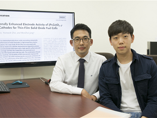 A New Efficient Oxide Coating Technology to Improve Fuel Cells
A new efficient oxide coating technology that can be applied in less than five minutes could lead to dramatic improvements in the lifetime and performance of fuel cells. The fundamental principle behind this approach is maximizing the oxygen reduction reaction site of a platinum thin-film electrode, preventing the electrodes from aggregating at high temperatures.
Fuel cells have emerged as a clean electricity generation system that does not pollute the air. In particular, solid oxide fuel cells (SOFCs) are beginning to gain a great deal of attention due to their higher power generation efficiency compared to other fuel cells. It is also advantageous to use other power sources than expensive hydrogen fuel.
However, the high costs and insufficient lifetimes caused by high temperatures needed to operate the solid oxide fuel cells have remained significant challenges to commercialization.
Recently, attempts to lower the operating temperature (< 600°C) of these devices by introducing thin-film processes have drew attention of researchers, with the resulting products known as thin-film-based solid oxide fuel cells.
In order to create enhanced device performance at lower temperatures, the research team, led by Professor WooChul Jung in the Department of Materials Science and Engineering, applied and developed oxide coating technology to maximize the oxygen reduction reaction sites of a platinum thin-film electrode and to prevent platinum electrodes from thermal aggregating.
The team succeeded in over-coating a platinum electrode with a new coating material called praseodymium-doped ceria (Pr,Ce)O2-, which has high conductivity for both electrons and oxygen ions and excellent catalytic properties for oxygen reduction reactions. As a result, electrode resistance was reduced by more than 1000 times, creating the potential for these electrodes to be used in high-temperature electrochemical cells.
In addition, they proposed that the high performance of thin-film-based oxide fuel cells’ oxygen electrodes could be realized through the nano-structuring of (Pr,Ce)O2-δ without any platinum.
Professor Jung said, “The electrode coating technology used in this study is of great technical value because of the utilization of affordable and mass-produced electrochemical deposition.” He added, “In the future, this technology will be feasible for replacing platinum electrodes in thin-film-based oxide fuel cells, and we expect that the affordable prices of this fuel cell will eventually boost market competitiveness.”
This research was described in Advanced Energy Materials in July and was featured as the Inside Front Cover and video abstract. It was supported by the Korea Institute of Energy Technology Evaluation and Planning (KETEP) and the Korea Electric Power Corporation (KEPCO) Research Institute.
Figure 1. The change of electrode activity with and without overcoated (Pr,Ce)O2-δ nanostructures.
2018.07.18 View 9253
 -
 Enhanced PDT to Cure Cancer with Fewer Side Effects
(From left: PhD candidate Ilkoo Noh and Professor Yeu-Chun Kim)
A KAIST research team developed near-infrared fluorophores-based photodynamic therapy (PDT) that reduced the downside of existing PDTs.
PDT is a way to cure wounds with lasers instead of drug treatment. When a laser irradiates a targeted site, a photosensitizer (PS) absorbs light energy and then converts oxygen to singlet oxygen or free radicals, leading to programmed cell death. This treatment has been used widely in clinical fields, especially for skin disease because it allows noninvasive treatment.
However, the existing PDTs have limitations for first-line therapy because PDT agents can cause genetic variations when they have low efficiency, hence reducing treatment effects.
The key to enhancing the efficiency of PDTs is how much PS can be concentrated to a wanted site, which laser wavelength the PS is reacted to, and how fast the PS clears organelle after treatment.
Professor Yeu-Chun Kim and his team from the Department of Chemical and Biomolecular Engineering, in collaboration with Professor Ji-Ho Park from the Department of Bio and Brain Engineering, developed a new PS called mitochondria targeting photodynamic therapeutic agent (MitDt) to maximize PDT effects while reducing unwanted side effects.
Mitochondria has emerged as target sites to maximize the effects of PS since they play essential roles in metabolism and have high transmembrane potential.
According to the team, when mitochondria is photodamaged by reactive oxygen species (ROS) generated after laser irradiation, they immediately lose their mitochondrial membrane potential and initiate apoptosis. Therefore, combining the PDT agent with the mitochondrial targeting agent can result in rapid damage to cancer cells, improving therapeutic efficacy and reducing unwanted side effects.
To successfully apply mitochondria-targeting PS, the team developed near-infrared (NIR) region PDT agents, which can be used to treat deep-tissue level cancer due to the permeability of the NIR laser. Light scattering is also decreased, thus obtaining higher therapeutic efficacy.
However, there is a problem of generating singlet oxygen when irradiating with an NIR laser. To address this issue, the team developed a novel PS that combines a functionalized NIR dye and a mitochondria-targeting agent to gain the benefit of rapid organelle clearance after treatment and also remain in cancer mitochondria for a long time, amplifying the amount of ROS to the target sites irradiated by the laser.
To verify the efficacy, the team injected MitDt into tumor-bearing mice. They were irradiated with an NIR laser at 662 nm to induce cancer treatment and their cancer size was reduced up to three-fold.
PhD candidate Ilkoo Noh, who led this research said, “This enhanced photodynamic cancer treatment has the advantage of treating a wanted site without any side effects because this PS stays longer in a mitochondrial cancer cell. We also confirmed that the PS did not cause cytotoxicity.”
Professor Kim added, “This research outcome will reduce the danger of side effects and can be applied for treating various diseases”.
This research was chosen as the cover page of Advanced Science on March 25.
Figure 1. The cover of Advanced Science
Figure 2. a) Chemical structure of MitDt compounds (above) b) mitochondria localization of designed PS (left) and ROS generation after 662nm laser irradiation (right)
2018.07.16 View 7542
 -
 KAIST Team Develops Flexible Blue Vertical Micro LEDs
A KAIST research team developed a crucial source technology that will advance the commercialization of micro LEDs.
Professor Keon Jae Lee from the Department of Materials Science and Engineering and his team have developed a low cost production technology for thin-film blue flexible vertical micro LEDs (f-VLEDs).
In CES 2018, micro LED TV was spotlighted as a strong candidate for replacing the active-matrix organic light-emitting diode (AMOLED) display. Micro LED is a sub-100 um light source for red, green and blue light, which has advantages of outstanding optical output, ultra-low power consumption, fast response speed, and excellent flexibility.
However, the current display industry has utilized the individual chip transfer of millions of LED pixels, causing high production cost. Therefore, the initial market of micro LED TV will be estimated to ~ a hundred thousand dollars for global premium market.
To widely commercialize micro LEDs for mobile and TV displays, the transfer method of thin film micro LEDs requires a one-time transfer of one million LEDs. In addition, highly efficient thin-film blue micro LED is crucial for a full-color display.
The team developed thin-film red f-VLED in previous projects, and now has realized thousands of thin-film blue vertical micro LEDs (thickness < 2 μm) on plastics using a one-time transfer.
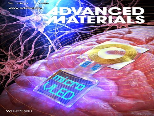
The blue GaN f-VLEDs achieved optical power density (~30 mW/mm2) three times higher than that of lateral micro LEDs, and a device lifetime of 100,000 hours by reducing heat generation. These blue f-VLEDs could be conformally attached to the curved skin and brains for wearable devices, and stably operated by wirelessly transferred electrical energy.
Professor Lee said, “For future micro LEDs, the innovative technology of thin-film transfer, efficient devices, and interconnection is necessary. We plan to demonstrate a full-color micro LED display in smart watch sizes by the end of this year. ”
This research “ Monolithic Flexible Vertical GaN Light‐Emitting Diodes for a Transparent Wireless Brain Optical Stimulator ” led by a PhD candidate Han Eol Lee was published in the June 2018 issue of Advanced Materials.
Figure 1. Schematic image of wireless thin-film blue f-VLED arrays on the brain surface
Figure 2. Photo of high-performance and high-density blue f-VLED arrays
2018.06.18 View 9536
 -
 Lead-free, Efficient Perovskite for Photovoltaic Cells
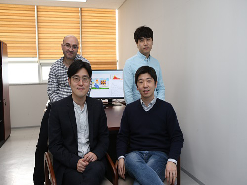
(Clockwise from left: Post-doc Researcher Lamjed Debbichi, Master’s Candidate Songju Lee, Professor Min Seok Jang and Professor Hyungjun Kim)
A KAIST research team has proposed a perovskite material, Cs2Au2I6 that serves as a potential active material for highly efficient lead-free thin-film photovoltaic devices. This material is expected to lay the foundation to overcome previously known limitations of perovskite including its stability and toxicity issues.
As strong candidates for next-generation high-efficiency photovoltaic cells, perovskite photovoltaic cells have a maximum photoconversion efficiency of 22%, comparable to high-performance crystalline silicon photovoltaic cells. In addition, perovskite-based cells can be fabricated at low temperatures, thereby bringing about dramatic cost reductions.
However, it has been noted that conventional organic-inorganic hybrid perovskite materials exhibit low stability, eventually degrading their performance and making them unfit for continued use. Moreover, their inclusion of lead has undermined their environmental friendliness.
In light of this, a joint team led by Professor Hyungjun Kim from the KAIST Department of Chemistry and Professor Min Seok Jang from the School of Electrical Engineering has analyzed a previously discovered perovskite material, Cs2Au2I6, consisting of only inorganic substances and investigated its suitability for application in thin-film photovoltaic devices. Theoretical investigations suggests that this new perovskite material is not only as efficient but also more stable and environment friendly compared to the conventional perovskite materials. For this analysis, the team developed multiscale multiphysics simulation frameworks. Atomic-scale first-principle quantum calculations were carried out to study the optical properties of the proposed material, and device-scale electromagnetic simulations were conducted to suggest that the material could indeed serve as a promising photovoltaic substance at the device level.
From this point onward, the research team plans to extend the study in two directions: an empirical study to apply the perovskite material in real-world photovoltaic cells and a theoretical analysis to find the optimal and highly stable material for photovoltaic cells. The team said, “Perovskite materials are highly efficient, but in order to completely replace the conventional solar cells, their stability and toxicity issues must first be resolved.” They added that this research is expected to accelerate related studies in pursuit of high-efficiency, environment-friendly perovskite materials.
This research, led by post-doc researcher Lamjed Debbichi and master’s candidate Songju Lee, was selected as the front cover article of Advanced Materials on March 22.
Figure 1. Cover of Advanced Materials
Figure 2. Schematic of full solar cell device structure
2018.06.08 View 10649
 -
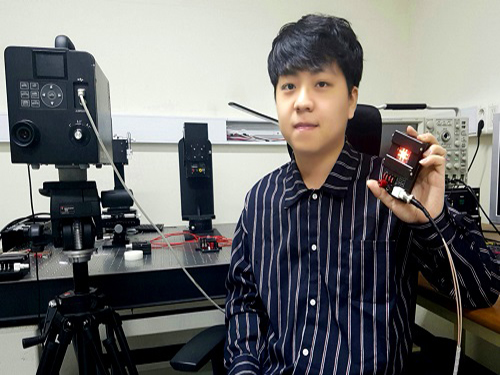 Get Treatment Anywhere and Any Time with Wearable PBM Patch
(PhD Candidate Yongmin Jeon)
There have been many cases in which OLEDs are applied to electronic devices, and now they have even been extended to therapeutic fields. A KAIST research team succeeded in developing a wearable photobiomodulation (PBM) patch to treat wounds. This technology will allow injuries to be treated regardless of location or time.
Professor KyungCheol Choi from the School of Electrical Engineering, in collaboration with Seoul National University Bundang Hospital’s team, conducted research on PBMs which are a clinical method widely used in hospitals. They are considered to be a safe, noninvasive, and nonsurgical method that require relatively low light power.
Conventionally, light-emitting diodes (LEDs) have been used in PBM applications; however, LED devices are usually inflexible and difficult to irradiate light uniformly. They may also produce localized heat. Due to these constraints, it was difficult to enhance the clinical effects of LED devices as they cannot stick to the human body.
Choi’s team developed a wearable patch using flexible OLEDs, allowing people to be treated outside of hospitals. A thin film has been developed for the patch, containing not only flexible OLEDs but also batteries and anti-superheating devices.
Moreover, its thickness is less than 1mm and its weight is less than 1g. This lightweight and ultra-thin patch with a bending radius is 20mm can be used more than 300 hours.
These patches are usable at a temperature below 42℃ to eliminate the risk of low-temperature burns. They also meet the safety regulations of the International Organization for Standardization (ISO) at red wavelengths (600–700 nm).
The wearable PBM patches showed excellent effects with in vitro wounds because they stimulated cell proliferation over 58% of control as well as cell migration over 46% of control under various conditions.
Yongmin Jeon, who led this research, said, “The wearable PBM is effective and convenient, so people can simply purchase it at a pharmacy without having to visit a hospital. If we can adjust the power and wavelength of the OLEDs, its application can be extended to skin care, cancer treatment, Alzheimer’s disease treatment, and mental healthcare.”
Professor Choi added, “We have applied the advantages of flexible OLEDs, which are often used for fabricating displays, to PBMs. This technology will open the way to commercialize portable and highly-efficient wearable photobiomodulation devices.”
This research was published in the front cover of Advanced Materials Technologies on May, 2018.
Figure 1. The patch attached to a human face, a hand and examples of treatment applications
Figure 2. The migration of cells into the scratched area
2018.05.25 View 8307
 -
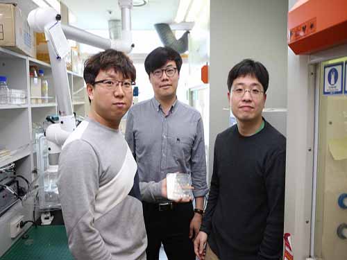 A High-Performance and Cost Effective Hydrogen Sensor
(Research team of Professor Park, Professor Jung, and research fellow Gao Min)
A KAIST research team reported a high-performance and cost effective hydrogen sensor using novel fabrication process based on the combination of polystyrene nanosphere lithography and semiconductor microfabrication processes.
The research team, led by Professor Inkyu Park in the Department of Mechanical Engineering and Professor Yeon Sik Jung in the Department of Materials Science and Engineering, fabricated a nanostructured high-performance hydrogen gas sensor based on a palladium-decorated silicon nanomesh structure made using a polystyrene nanosphere self-assembly method. Their study was featured as the front cover article of journal “Small” (Publisher: Wiley-VCH) on March 8, 2018.
The nanosphere lithography method utilizes the self-assembly of a nanosphere monolayer. This could be an alternative choice for achieving uniform and well-ordered nanopatterns with minimum sub-10 nanometer dimensions. The research team said that the small dimensions of the silicon enhanced the palladium-gating effect and thus dramatically improved the sensitivity.
Hydrogen gas is widely considered to be one of the most promising next-generation energy resources. Also, it is a very important material for various industrial applications such as hydrogen-cooled systems, petroleum refinement, and metallurgical processes. However, hydrogen, which is highly flammable, is colorless and odorless and thus difficult to detect with human senses. Therefore, developing hydrogen gas sensors with high sensitivity, fast response, high selectivity, and good stability is of significant importance for the rising hydrogen economy.
Silicon nanowire-based devices have been employed as efficient components in high-performance sensors for detecting gases and other chemical and biological components. Since the nanowires have a high surface-to-volume ratio, they respond more sensitively to the surrounding environment.
The research team’s gas sensor shows dramatically improved hydrogen gas sensitivity compared with a silicon thin film sensor without nanopatterns. Furthermore, a buffered oxide etchant (BOE) treatment of the silicon nanomesh structure results in an additional performance improvement through suspension of nanomesh strutures from the substrate and surface roughening. The sensor device shows a fast hydrogen response (response time < 5 seconds) and 10 times higher selectivity to hydrogen gas among other gases. Their sensing performance is stable and shows repeatable responses in both dry and high-humidity ambient environments.
Professor Park said that his approach will be very useful for the fabrication of low-cost, high-performance sensors for chemical and biological detection with applications to mobile and wearable devices in the coming era of internet of things (IoTs).
(Figure 1: The front cover image of Small dated on March 8.)
(Figure 2: Gas sensor responses upon the exposure to H2 at various concentrations.)
2018.05.21 View 10345
 -
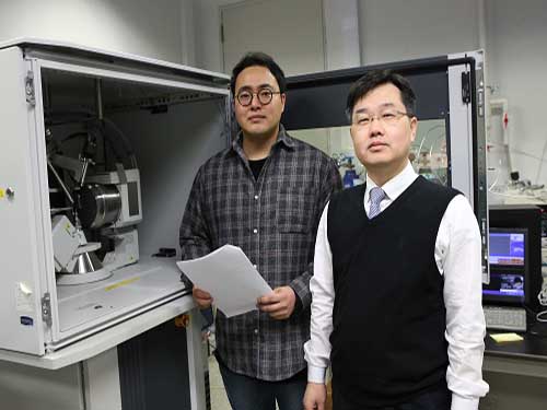 Aqueous Storage Device Needs Only 20 Seconds to Go
(from left: PhD candidate Il Woo Ock and Professor Jeung Ku Kang)
A KAIST research team developed a new hybrid energy storage device that can be charged in less than half a minute. It employs aqueous electrolytes instead of flammable organic solvents, so it is both environmentally friendly and safe. It also facilitates a boosting charge with high energy density, which makes it suitable for portable electronic devices.
Professor Jeung Ku Kang and his team from the Graduate School of Energy, Environment, Water, and Sustainability developed this hybrid energy storage with high energy and power densities along over a long cycle life by assembling fibre-like polymer chain anodes and sub-nanoscale metal oxide cathodes on graphene.
Conventional aqueous electrolyte-based energy storage devices have a limitation for boosting charges and high energy density due to low driving voltage and a shortage of anode materials.
Energy storage device capacity is determined by the two electrodes, and the balance between cathode and anode leads to high stability. In general, two electrodes show differences in electrical properties and differ in ion storage mechanism processes, resulting in poor storage and stability from the imbalance.
The research team came up with new structures and materials to facilitate rapid speed in energy exchange on the surfaces of the electrodes and minimize the energy loss between the two electrodes.
The team made anodes with graphene-based polymer chain materials. The web-like structure of graphene leads to a high surface area, thereby allowing higher capacitance.
For cathode materials, the team used metal oxide in sub-nanoscale structures to elevate atom-by-ion redox reactions. This method realized higher energy density and faster energy exchange while minimizing energy loss.
The developed device can be charged within 20 to 30 seconds using a low-power charging system, such as a USB switching charger or a flexible photovoltaic cell. The developed aqueous hybrid energy device shows more than 100-fold higher power density compared to conventional aqueous batteries and can be rapidly recharged. Further, the device showed high stability with its capacity maintained at 100% at a high charge/discharge current.
Professor Kang said, “This eco-friendly technology can be easily manufactured and is highly applicable. In particular, its high capacity and high stability, compared to existing technologies, could contribute to the commercialization of aqueous capacitors. The device can be rapidly charged using a low-power charging system, and thus can be applied to portable electronic device.”
This research, led by a PhD candidate Il Woo Ock, was published in Advanced Energy Materials on January 15.
Figure 1. Switching wearable LED kit with two AHCs in series charged by a flexible photovoltaic cell
Figure 2. Schematic diagram for aqueous hybrid capacitors
Figure 3. TEM images of anode and cathode
2018.02.28 View 13559
 -
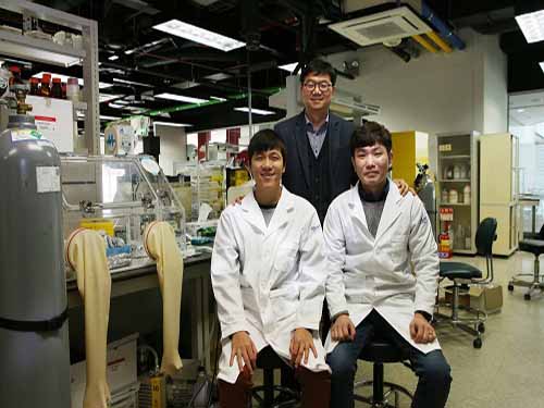 Low-power, Flexible Memristor Circuit for Mobile and Wearable Devices
(from left: Yunyong Nam, Professor Sung-Yool Choi and Byung Chul Jang)
A KAIST research team succeeded in developing an energy efficient, nonvolatile logic-in-memory circuit by using a memristor. This novel technology can be used as an energy efficient computing architecture for battery-powered flexible electronic systems, such as mobile and wearable devices.
Professor Sung-Yool Choi from the School of Electrical Engineering and Professor Sang-Hee Ko Park from the Department of Materials Science and Engineering developed a memristive nonvolatile logic-in-memory circuit.
Transistor-based conventional electronic systems have issues with battery supply and a long standby period due to their volatile computing architecture. The standby power consumption caused by subthreshold leakage current limits their potential applications for mobile electronic devices. Also, their physical separation of memory and processor causes power consumption and time delay during data transfer.
In order to solve this problem, the team developed a logic-in-memory circuit that enables data storage as well as logic operation simultaneously. It can minimize energy consumption and time delay because it does not require data transfer between memory and processor.
The team employed nonvolatile, polymer-based memristors and flexible back-to-back Schottky diode selector devices on plastic substrates. Unlike the conventional architecture, this memristive nonvolatile logic-in-memory is a novel computing architecture that consumes a minimal amount of standby power. This one-selector-one memristor (1S-1M) solved the issue of undesirable leakage currents, known as ‘sneak currents’.
They also implemented single-instruction multiple-data (SIMD) to calculate multiple values at once.
The proposed parallel computing method using a memristive nonvolatile logic-in-memory circuit can provide a low-power circuit platform for battery-powered flexible electronic systems with a variety of potential applications.
Professor Choi said, “Flexible logic-in-memory circuits integrating memristor and selector device can provide flexibility, low power, memory with logic functions. This will be a core technology that will bring innovation to mobile and wearable electronic systems.”
This research, collaborated with Ph.D. candidates Byung Chul Jang and Yunyong Nam, was published and chosen as the cover of Advanced Functional Materials on January 10.
Figure 1. Cover of the Advanced Functional Materials
Figure 2. Schematic illustration and cross-sectional TEM image of flexible memristive nonvolatile logic-in-memory circuit
Figure 3. Test performance
Figure 4. Parallel logic operation within 1S-1M memristor array
2018.02.21 View 7397
 -
 Realizing Highly Efficient Quantum Dot LEDs with Metallic Nanostructures
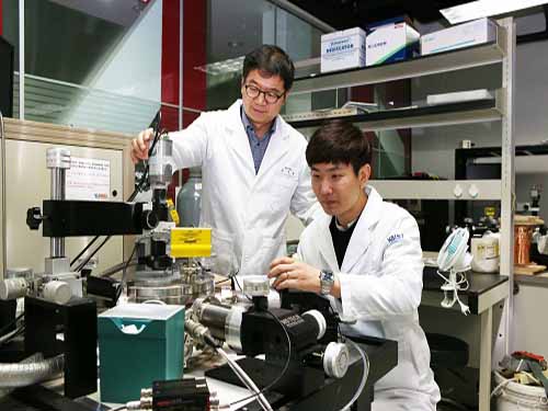
(Professor Yong-Hoon Cho and PhD candidate Hyun Chul Park)
KAIST researchers have discovered a technology that enhances the efficiency of Quantum Dot LEDs.
Professor Yong-Hoon Cho from the Department of Physics and his team succeeded in improving the efficiency of Quantum Dot (QD) Light-Emitting Diodes (LEDs) by designing metallic nanostructure substrates.
QD LEDs possess very small semiconductor light sources and are considered to be the new rising technology for high performance full-color display. However, it is expensive to manufacture displays with QD LED only.
Existing QD-based displays use blue LEDs as a source of light, and they employ a method of color conversion through excitation of green and red QDs.
There are two inconveniences with the existing QD-based displays. As mentioned previously, QD LED is costly, hence the unit price of QD-based displays is higher. Also, the efficiency of a liquid type of QDs is drastically lowered after contact with air.
Professor Cho found the solution in a metallic nanostructure for lowering the production cost while improving the efficiency of QD LEDs.
The team exploited the phenomenon of so-called surface plasmonic resonances when nanoscale metallic structures are exposed to light. Depending on the metal, the size, and the shape, the properties of metallic structures vary.
The team used different metallic nanostructures for each QD LED – silver nanodisks for Red QDs and aluminum nanodisks for Green GDs – to make them more fluorescent.
With brighter QDs, it requires fewer QDs to manufacture QD LEDs, contributing to a lower unit price.
The team used silver and aluminum in this research, but metallic nanostructures can be redesigned according to the desired purposes.
Professor Cho said, “Implementing metallic nanostructures into QD LEDs in a proper manner can reduce the quantity of the QDs required for the system, leading to lower unit prices.”
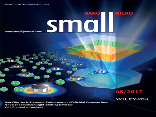
This research, led by PhD candidate Hyun Chul Park, was chosen as the cover of the international journal, Small, on December 27, 2017.
Figure 1. Cover of the journal
Figure 2. Spectrum showing different fluorescence with and without metallic nanostructure
2018.01.23 View 7819
 -
 Ultra-Low Power Flexible Memory Using 2D Materials
(Professor Choi and Ph.D. candidate Jang)
KAIST research team led by Professor Sung-Yool Choi at School of Electrical Engineering and Professor Sung Gap Im at the Department of Chemical and Biomolecular Engineering developed high-density, ultra-low power, non-volatile, flexible memory technology using 2D materials. The team used ultrathin molybdenum disulfide (MoS2) with atomic-scale thickness as the channel material and high-performance polymeric insulator film as the tunneling dielectric material. This research was published on the cover of Advanced Functional Materials on November 17. KAIST graduate Myung Hun Woo, a researcher at Samsung Electronics and Ph.D. candidate Byung Chul Jang are first authors.
The surge of new technologies such as Internet of Things (IoT), Artificial Intelligence (AI), and cloud server led to the paradigm shift from processor-centric computing to memory-centric computing in the industry, as well as the increase in demand of wearable devices. This led to an increased need for high-density, ultra-low power, non-volatile flexible memory. In particular, ultrathin MoS2 as semiconductor material has been recently regarded as post-silicon material. This is due to its ultrathin thickness of atomic-scale which suppresses short channel effect observed in conventional silicon material, leading to advantages in high- density and low-power consumption. Further, this thickness allows the material to be flexible, and thus the material is applicable to wearable devices.
However, due to the dangling-bond free surface of MoS2 semiconductor material, it is difficult to deposit the thin insulator film to be uniform and stable over a large area via the conventional atomic layer deposition process. Further, the currently used solution process makes it difficult to deposit uniformly low dielectric constant (k) polymeric insulator film with sub-10 nm thickness on a large area, thus indicating that the memory device utilizing the conventional solution-processed polymer insulator film cannot be operated at low-operating voltage and is not compatible with photolithography.
The research team tried to overcome the hurdles and develop high-density, ultra-low power, non-volatile flexible memory by employing a low-temperature, solvent-free, and all-dry vapor phase technique named initiated chemical vapor deposition (iCVD) process. Using iCVD process, tunneling polymeric insulator film with 10 nm thickness was deposited uniformly on MoS2 semiconductor material without being restricted by the dangling bond-free surface of MoS2. The team observed that the newly developed MoS2-based non-volatile memory can be operated at low-voltage (around 10V), in contrast to the conventional MoS2-based non-volatile memory that requires over 20V.
Professor Choi said, “As the basis for the Fourth Industrial revolution technologies including AI and IoT, semiconductor device technology needs to have characteristics of low-power and flexibility, in clear contrast to conventional memory devices.” He continued, “This new technology is significant in developing source technology in terms of materials, processes, and devices to contribute to achieve these characteristics.”
This research was supported by the Global Frontier Center for Advanced Soft Electronics and the Creative Materials Discovery Program by funded the National Research Foundation of Korea of Ministry of Science and ICT.
( Figure 1. Cover of Advanced Functional Materials)
(Figure 2. Concept map for the developed non-volatile memory material and high-resolution transmission electron microscopy image for material cross-section )
2018.01.02 View 11057
 -
 Platinum Single Atom Catalysts for 'Direct Formic Acid Fuel Cells'
(Professor Hyunjoo Lee (left) and Ph.D. candidate Jiwhan Kim)
A research team co-led by Professor Hyunjoo Lee at the Department of Chemical and Biomolecular Engineering at KAIST and Professor Jeong Woo Han from the University of Seoul synthesized highly stable high-Pt-content single atom catalysts for direct formic acid fuel cells. The amount of platinum can be reduced to 1/10 of that of conventional platinum nanoparticle catalysts.
Platinum (Pt) catalysts have been used in various catalytic reactions due to their high activity and stability. However, because Pt is rare and expensive, it is important to reduce the amount of Pt used. Pt single atom catalysts can reduce the size of the Pt particles to the size of an atom. Thus, the cost of Pt catalysts can be minimized because all of the Pt atoms can participate in the catalytic reactions. Additionally, single atom catalysts have no ensemble site in which two or more atoms are attached, and thus, the reaction selectivity is different from that of nanoparticle catalysts.
Despite these advantages, single atom catalysts are easily aggregated and less stable due to their low coordination number and high surface free energy. It is difficult to develop a single atom catalyst with high content and high stability, and thus, its application in practical devices is limited.
Direct formic acid fuel cells can be an energy source for next-generation portable devices because liquid formic acid as a fuel is safer and easier to store and transport than high-pressure hydrogen gas.
To improve the stability of Pt single atom catalysts, Professor Lee’s group developed a Pt-Sn single atom alloy structure on an antimony-doped tin oxide (ATO) support. This structure has been proven by computational calculations which show that Pt single atoms substitute antimony sites in the antimony-tin alloy structure and are thermodynamically stable. This catalyst has been shown to have a higher activity up to 50 times per weight of Pt than that of the commercial catalyst, Pt/C, in the oxidation of formic acid, and the stability of the catalyst was also remarkably high.
Professor Lee’s group also used a single atomic catalyst in a 'direct formic acid fuel cell’ consisting of membranes and electrodes. It is the first attempt to apply a single atomic catalyst to a full cell. In this case, an output similar to that of the commercial catalyst could be obtained by using 1/10 of the platinum compared to the commercial Pt/C catalyst.
Ph.D. candidate Jiwhan Kim from KAIST was the first author of the research. This research was published online on September 11 in Advanced Energy Materials.
This research was carried out with the support of the Samsung Electronics Future Technology Development Center.
(Figure 1. Concept photograph for Pt single atom catalysts.)
(Figure 2. Pt single atom catalysts by HAADF-STEM analysis (bright white circles))
2017.10.31 View 8420