CES
-
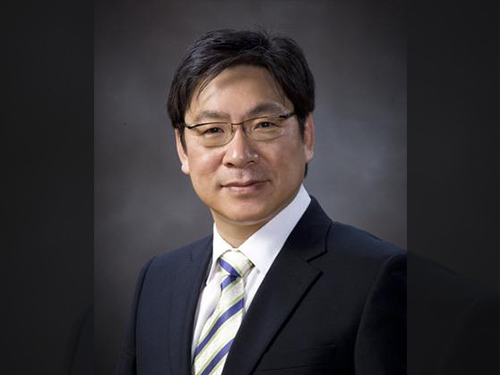 Professor Key-Sun Choi Receives the Order of Service Merit Green Stripes from the Korean Government
The award recognizes Professor Choi’s life-long research effort to make Korean language digitally available, both nationally and internationally.
Professor Key-Sun Choi of the School of Computing at KAIST received the Order of Service Merit Green Stripes from the Korean government at the 569th Korean Language Day, held annually to commemorate the invention of the Korean language, Hangeul. The ceremony took place on October 9, 2015, at the Sejong Center in Seoul.
Professor Choi has distinguished himself in the field of natural language processing (NLP), including Korean language. He developed a Korean NLP parser that enabled information processing and data analysis of Korean language, as well as a digital Korean dictionary, contributing to the advancement of Korean language-based information technology.
Professor Choi also led the way to widespread use of Korean natural language in computing by developing and commercializing open source software to process the Korean language.
He has served leading roles in many of the international academic societies and standardization organizations, among others, as the vice president of Infoterm (the International Information Center for Terminology), president of the Asia Federation of Natural Language Processing, vice chair of ISO/TC 37, a technical committee in the International Organization for Standardization (ISO), and a council member for the International Association of Machine Translation.
2015.10.08 View 9471
 -
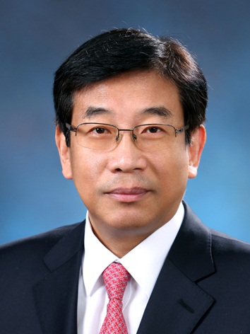 Professor Jae Kyu Lee Appointed the President of Association for Information Systems
Chair Professor Jae Kyu Lee of KAIST’s College of Business was appointed the President of Association for Information Systems (AIS) on July 1, 2015. Professor Lee will serve a one-year term, which will end in June 2016. With four thousand members researching information systems from 90 different nations, AIS is the largest academic society in the fields of information system and business process engineering.
Professor Lee has proposed his idea of “the Bright Internet” as the official vision of AIS. Employing this vision, AIS will create technology and systems, as well as sponsor international cooperation to solve fundamental issues of the Internet including concerns over hacking and cyber-related crimes.
The extent of damage from cyber-related crimes grows each year. Every day, 56 billion junk emails are sent to computers which are hacked and become “zombie” computers. The social cost of such crimes is estimated to be 400 billion US dollars annually.
Based on "the Bright Internet," AIS will build a preventative Internet security system by adopting ground rules that make attackers responsible for the damages from such crimes. The system will also modify technology and other systems to minimize privacy infringement while maintaining security. Finally, the Bright Internet proposes to adopt an international standard for this security system through collaboration with the International Telecommunications Union (ITU).
Professor Lee said, “The vision of the Bright Internet started from an awareness that we needed to resolve issues such as Internet addiction, indiscriminate media exposure, and verbal violence. This vision developed by the experts from all around the world will not only bring a revolution of a reliable Internet platform to a global scale but also reshape the Korean Internet platform.”
2015.07.02 View 8362
 -
 Professor Naehyuck Jang was Appointed Technical Program Chair of the Design Automation Conference
Professor Naehyuck Jang of the Electrical Engineering Department at KAIST was appointed as the technical program chair of the Design Automation Conference (DAC). He is the first Asian to serve the conference as the chair. At next year’s conference, he will select 150 program committee members and supervise the selection process of 1,000 papers.
Founded in 1964, DAC encompasses research related to automation of semiconductor processes, which usually involve billions of transistors. More than seven thousand people and 150 companies from all around the world participate, of which only the top 20% of the submitted papers are selected. It is the most prestigious conference in the field of semiconductor automation.
The Design Automation Conference also introduces optimization and automation of design processes of systems, hardware security, automobiles, and the Internet of things. Professor Jang specializes in low power system designs. As an ACM Distinguished Scientist, Professor Jang was elected as the chairman after contributing to this year’s program committee by reforming the process of selection of papers.
Professor Jang said, “This year’s conference represents a departure, where we move from the field of traditional semiconductors to the optimization of embedded system, the Internet of things, and security. He added that “we want to create a paper selection process that can propose the future of design automation.”
The 53rd annual DAC will take place at the Austin Convention Center in Texas in June 2016.
2015.07.02 View 7492
 -
 KAIST Team Develops Flexible PRAM
Phase change random access memory (PRAM) is one of the strongest candidates for next-generation nonvolatile memory for flexible and wearable electronics. In order to be used as a core memory for flexible devices, the most important issue is reducing high operating current. The effective solution is to decrease cell size in sub-micron region as in commercialized conventional PRAM. However, the scaling to nano-dimension on flexible substrates is extremely difficult due to soft nature and photolithographic limits on plastics, thus practical flexible PRAM has not been realized yet.
Recently, a team led by Professors Keon Jae Lee and Yeon Sik Jung of the Department of Materials Science and Engineering at KAIST has developed the first flexible PRAM enabled by self-assembled block copolymer (BCP) silica nanostructures with an ultralow current operation (below one quarter of conventional PRAM without BCP) on plastic substrates. BCP is the mixture of two different polymer materials, which can easily create self-ordered arrays of sub-20 nm features through simple spin-coating and plasma treatments. BCP silica nanostructures successfully lowered the contact area by localizing the volume change of phase-change materials and thus resulted in significant power reduction. Furthermore, the ultrathin silicon-based diodes were integrated with phase-change memories (PCM) to suppress the inter-cell interference, which demonstrated random access capability for flexible and wearable electronics. Their work was published in the March issue of ACS Nano: "Flexible One Diode-One Phase Change Memory Array Enabled by Block Copolymer Self-Assembly."
Another way to achieve ultralow-powered PRAM is to utilize self-structured conductive filaments (CF) instead of the resistor-type conventional heater. The self-structured CF nanoheater originated from unipolar memristor can generate strong heat toward phase-change materials due to high current density through the nanofilament. This ground-breaking methodology shows that sub-10 nm filament heater, without using expensive and non-compatible nanolithography, achieved nanoscale switching volume of phase change materials, resulted in the PCM writing current of below 20 uA, the lowest value among top-down PCM devices. This achievement was published in the June online issue of ACS Nano: "Self-Structured Conductive Filament Nanoheater for Chalcogenide Phase Transition." In addition, due to self-structured low-power technology compatible to plastics, the research team has recently succeeded in fabricating a flexible PRAM on wearable substrates.
Professor Lee said, "The demonstration of low power PRAM on plastics is one of the most important issues for next-generation wearable and flexible non-volatile memory. Our innovative and simple methodology represents the strong potential for commercializing flexible PRAM."
In addition, he wrote a review paper regarding the nanotechnology-based electronic devices in the June online issue of Advanced Materials entitled "Performance Enhancement of Electronic and Energy Devices via Block Copolymer Self-Assembly."
Picture Caption:
Low-power nonvolatile PRAM for flexible and wearable memories enabled by (a) self-assembled BCP silica nanostructures and (b) self-structured conductive filament nanoheater.
2015.06.15 View 15663
 -
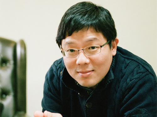 Science and Technology Policy Professor Chihyung Jeon Awarded Rachel Carson Fellowship
KAIST Graduate School of Science and Technology Policy Professor Chihyung Jeon has been awarded the Rachel Carson Fellowship 2015-2016.
Rachel Carson Center for Environment and Society is a research center for environmental humanities and social sciences, supported by the German Federal Ministry of Education and Research. It was founded by Ludwig-Maximilians-Universität, Munich, Germany and the Deutsches Museum as a joint initiative in 2009.
Rachel Carson Center supports researches in humanities and social sciences on the interactions between the environment and the society, following the footsteps of Rachel Cason, who raised awareness on the chemical environmental damage and started global environmental movement through her published book “Silent Spring” in 1962.
The center is awarding Rachel Carson Fellowships to established researchers to fund their writing and promote exchange of research. This year, 31 fellowships were awarded.
Professor Jeon will conduct research on "A Dredged Nation: The Four Rivers Restoration Project and the Envirotechnical Transformation of South Korea" and will also hold an additional post of International Curatorial Fellow at the Deutsches Museum.
2015.06.11 View 10671
 -
 KAIST's Patina Engraving System Awarded at ACM CHI
Professor Tek-Jin Nam’s research team of the Industrial Design Department of KAIST received the Best Paper Award in the 2015 Association for Computing Machinery’s (ACM) Conference on Human Factors in Computing Systems (CHI) which was held from April 18 to 23, 2015. The team consisted of two KAIST students: Moon-Hwan Lee, a Ph.D. candidate, and Sejin Cha, a master's student. The team was the first in Asia to receive the award.
The ACM CHI represents the premier conference in the field of Human-Computer Interaction (HCI). This year’s event, held in Seoul, South Korea, was the first conference that the ACM had held in Asia in its thirty-three year history. The KAIST team’s paper, entitled “Patina Engraver: Visualizing Activity Logs as Patina in Fashionable Trackers,” ranked in the top 1% of 2,000 submitted papers.
The team developed Patina Engraver, an activity tracker, which monitors and tracks fitness-related metrics such as distances walked or run, calorie consumption, heartbeat, sleep quality, and blood pressure. The device wirelessly connects to a computer or smartphone so that it can store and utilize long-term tracking data.
However, what makes Patina Engraver, a smart wristband, different from other health trackers is its ability to display different design patterns based on users’ activity on the surface of the wristband. The research team was inspired to build this system from the fact that wearable electronics including activity trackers can be used not only as health care devices, but also as fashion items to express emotions and personalities.
Equipped with an engraving feature, the charging pad or holder for Patina Engraver draws individualized patterns to reflect the user’s activities, such as walking or running, while the device is being charged. The pattern display syncs with the frequency of usage, therefore, the more the tracker is used, the greater the number of patterns will show up.
According to the team, since Patina Engraver provides users with a personalized illustration of their activity on the tracker, users are more motivated to put on the tracker and exercise.
Professor Nam said, “This research can be applied in producing other wearable devices to enhance users’ emotional satisfaction. When wearable technology is combined with design and emotion, the industry market will quickly expand.”
Figure 1: Patina engraving system developed by KAIST research team
Figure 2: The process of engraving illustrations of the activity records onto the tracker
Figure 3: Personalized activity trackers based on activity records
2015.05.15 View 14499
 -
 Professor Sang Ouk Kim Receives the POSCO Academic Award
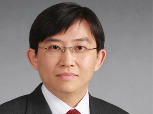
Professor Sang Ouk Kim of KAIST’s Department of Materials Science and Engineering received the 2015 POSCO Academic Award. The award ceremony took place at the annual conference of the Korean Institute of Metals and Materials on April 23, 2015.
The POSCO Academic Award has been presented to the Institute's researchers and academics in recognition of their contributions to the advancement of metals and materials engineering in Korea.
Professor Kim is known for his pioneering work in manipulating the properties (work function, conductivity, surface energy, chemo-responsiveness, etc.) of carbon-based materials using double-element doping. Through his research, Professor Kim showed that carbon materials could be extremely useful in various areas including solar batteries and flexible devices. His work has been recognized and published in such journals as Advanced Materials, which invited him to write a review paper on his research in its 25th anniversary issue in 2014, along with world-renowned scholars including the Nobel laureate Alan Heeger.
Professor Kim has published a total of 143 Science Citation Index papers in journals like Nature, Science, Nature Materials, Nature Communications, Advanced Materials, Nano Letters, and Physical Review Letters. According to Scopus, a bibliographic database containing abstracts and citations for academic journal articles, he has been cited 6,456 times and has the h-index of 44, an index describing the scientific productivity and impact of a researcher.
2015.04.22 View 10819
 -
 KAIST Develops a Credit-Card-Thick Flexible Lithium Ion Battery
Since the battery can be charged wirelessly, useful applications are expected including medical patches and smart cards.
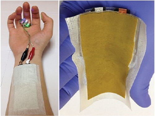
Professor Jang Wook Choi at KAIST’s Graduate School of Energy, Environment, Water, and Sustainability (EEWS) and Dr. Jae Yong Song at the Korea Research Institute of Standards and Science jointly led research to invent a flexible lithium ion battery that is thinner than a credit card and can be charged wirelessly.
Their research findings were published online in Nano Letters on March 6, 2015. Lithium ion batteries are widely used today in various electronics including mobile devices and electronic cars. Researchers said that their work could help accelerate the development of flexible and wearable electronics.
Conventional lithium ion batteries are manufactured based on a layering technology, stacking up anodes, separating films, and cathodes like a sandwich, which makes it difficult to reduce their thickness. In addition, friction arises between layers, making the batteries impossible to bend. The coating films of electrodes easily come off, which contributes to the batteries’ poor performance.
The research team abandoned the existing production technology. Instead, they removed the separating films, layered the cathodes and anodes collinearly on a plane, and created a partition between electrodes to eliminate potential problems, such as short circuits and voltage dips, commonly present in lithium ion batteries.
After more than five thousand consecutive flexing experiments, the research team confirmed the possibility of a more flexible electrode structure while maintaining the battery performance comparable to the level of current lithium ion batteries.
Flexible batteries can be applied to integrated smart cards, cosmetic and medical patches, and skin adhesive sensors that can control a computer with voice commands or gesture as seen in the movie “Iron Man.”
Moreover, the team has successfully developed wireless-charging technology using electromagnetic induction and solar batteries.
They are currently developing a mass production process to combine this planar battery technology and printing, to ultimately create a new paradigm to print semiconductors and batteries using 3D printers.
Professor Choi said, “This new technology will contribute to diversifying patch functions as it is applicable to power various adhesive medical patches.”
Picture 1: Medical patch (left) and flexible secondary battery (right)
Picture 2: Diagram of flexible battery
Picture 3: Smart card embedding flexible battery
2015.03.24 View 13078
 -
 Interactions Features KAIST's Human-Computer Interaction Lab
Interactions, a bi-monthly magazine published by the Association for Computing Machinery (ACM), the largest educational and scientific computing society in the world, featured an article introducing Human-Computer Interaction (HCI) Lab at KAIST in the March/April 2015 issue (http://interactions.acm.org/archive/toc/march-april-2015).
Established in 2002, the HCI Lab (http://hcil.kaist.ac.kr/) is run by Professor Geehyuk Lee of the Computer Science Department at KAIST. The lab conducts various research projects to improve the design and operation of physical user interfaces and develops new interaction techniques for new types of computers. For the article, see the link below:
ACM Interactions, March and April 2015
Day in the Lab: Human-Computer Interaction Lab @ KAIST
http://interactions.acm.org/archive/view/march-april-2015/human-computer-interaction-lab-kaist
2015.03.02 View 10917
 -
 KAIST Develops Subminiature, Power-Efficient Air Pollution Sensing Probe
Professor Inkyu Park and his research team from the Department of Mechanical Engineering at KAIST have developed a subminiature, power-efficient air-pollution sensing probe that can be applied to mobile devices. Their research findings were published online in the January 30th issue of Scientific Reports.
As air pollution has increased, people have taken greater interest in health care. The developed technology could allow people to measure independently the air pollution level of their surrounding environments.
Previous instruments used to measure air pollution levels were bulky and consumed a lot of power. They also often produced inaccurate results when measuring air pollution in which different toxic gases were mixed. These problems could not be resolved with existing semiconductor manufacturing process.
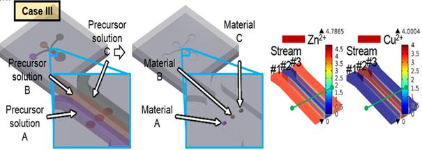
Using local temperature field control technology, Professor Park’s team succeeded in integrating multiple heterogeneous nanomaterials and fitting them onto a small, low-power electronic chip. This microheating sensor can heat microscale regions through local hydrothermal synthesis. Because it requires a miniscale amount of nanomaterials to manufacture, the sensor is most suitable for mobile devices.
Professor Park said, “Our research will contribute to the development of convergence technology in such field as air pollution sensing probes, biosensors, electronic devices, and displays.”
The team's research was supported by the Ministry of Education and the Ministry of Science, ICT and Future Planning, Republic of Korea.
Figure 1 – The Concept of Multiple Nanomaterial Device and Numerical Simulation Results of Precursor Solutions
Figure 2 - Multiple Nanomaterial Manufactured in a Microscale Region
2015.02.27 View 11371
 -
 KAIST's Thermoelectric Generator on Glass Fabric Receives the Grand Prize at the Netexplo Forum 2015
The forum announced top ten IT innovations expected to change the world and selected the grand prize on February 4, 2014.
Established in 2007 by Martine Bidegain and Thierry Happe in partnership with the French Senate and the French Ministry for the Digital Economy, the Netexplo Observatory is an independent global organization that studies the impact of digital technology and innovation on society and business.
Every year, the Netexplo Observatory hosts an international conference, the Netexplo Forum, in Paris, France, which surveys digital innovation worldwide. The 8th forum was held in partnership with the United Nations Educational, Scientific and Cultural Organization (UNESCO) on February 4-5, 2015, at the UNESCO House in Paris.
Prior to the conference, the Netexplo Forum 2015 named the top ten most promising digital technologies that will greatly impact the world.
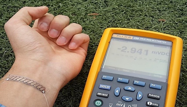
Among them was Professor Byung Jin Cho’s research on a wearable thermoelectric generator (http://www.eurekalert.org/pub_releases/2014-04/tkai-tgo041014.php). The generator was selected as the most innovative technology this year.
Professor Cho of KAIST’s Electrical Engineering Department developed a glass fabric-based thermoelectric generator that is extremely light and flexible and that produces electricity from the heat of the human body. This technology can be applied widely to wearable computers and mobile devices.
The full list of innovations follows below:
Wearable Thermo-Element, South Korea: The human body becomes a source of energy for mobile devices.
W.Afate 3D-printer, Togo: An environmentally friendly fablab that makes a low-cost 3D-printer from recycling electronic components.
Slack, USA: By combining email, Skype, and file-sharing and social networks, internal communication becomes much easier and simpler.
PhotoMath, Croatia: A free app that enables smartphone users to solve mathematical problems simply by scanning the mathematical texts.
Kappo, Chile: Connected cyclists produce and transmit useful data for urban planning to make the city more bike-friendly.
Branching Minds, USA: An improved learning process for students in difficulty through a personalized approach.
Baidu Kuai Sou, China: Smart chopsticks that can check food hazards.
SCio, Israel: A pocket molecular sensor with various applications and data
Rainforest Connection, USA: Fighting deforestation with recycled smartphones
Sense Ebola Followup, Nigeria: A mobile tool to help contain Ebola
For more details on the wearable thermos-element which received the 2015 Netexplo Award, please go to https://www.netexplo.org/en/intelligence/innovation/wearable-thermo-element.
Pictures 1 and 2: A high-performance wearable thermoelectric generator that is extremely flexible and light.
Picture 3: Senator Catherine Morin-Desailly (left) of the French Parliament presents the 2015 Netexplo Award to Professor Byung Jin Cho (right) on February 4, 2015 at the UNESCO House in Paris.
Credit of Loran Dhérines
Picture 4: Professor Byung Jin Cho (left) poses with Dr. Joël de Rosnay (right).
Credit of Loran Dhérines
2015.02.06 View 15050
 -
 Press Release on Piezoelectric Nanogenerators of ZnO with Aluminium Nitride Stacked Layers by the American Institute of Physics
The
American Institute of Physics (AIP) released a news article entitled “Zinc
Oxide Materials Tapped for Tiny Energy Harvesting Devices” on January 13, 2015.
The
article described the research led by Professor Giwan Yoon of the
Electrical Engineering Department at KAIST. It was published in the January
12, 2015 issue of Applied Physics Letters.
AIP publishes the journal. For the news release, please visit the
link below:
The American
Institute of Physics, January 13, 2015
“Zinc
Oxide Materials Tapped for Tiny Energy Harvesting Devices”
New research helps
pave the way toward highly energy-efficient zinc oxide-based micro energy
harvesting devices with applications in portable communications, healthcare and
environmental monitoring, and more
http://www.aip.org/publishing/journal-highlights/zinc-oxide-materials-tapped-tiny-energy-harvesting-devices
2015.02.04 View 33580