Keon+Jae+Lee
-
 AI-Driven Wearable Blood Pressure Sensor for Continuous Health Monitoring – Published in Nature Reviews Cardiology
A KAIST research team led by Professor Keon Jae Lee has proposed an innovative theoretical framework and research strategies for AI-based wearable blood pressure sensors, paving the way for continuous and non-invasive cardiovascular monitoring.
Hypertension is a leading chronic disease affecting over a billion people worldwide and is a major risk factor for severe cardiovascular conditions such as myocardial infarction, stroke, and heart failure. Traditional blood pressure measurement relies on intermittent, cuff-based methods, which fail to capture real-time fluctuations and present challenges in continuous patient monitoring.
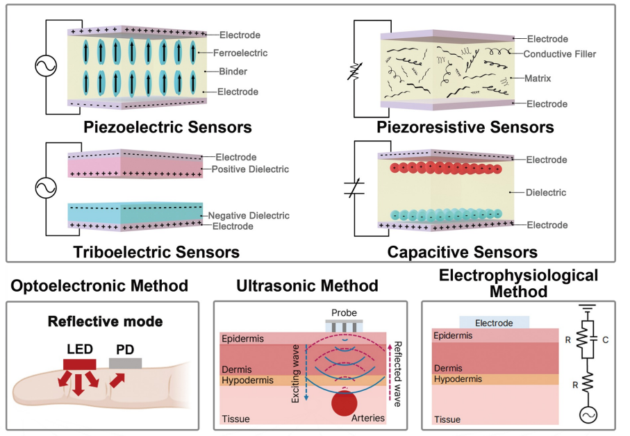
Wearable blood pressure sensors offer a non-invasive solution for continuous blood pressure monitoring, enabling real-time tracking and personalized cardiovascular health management. However, current technologies lack the accuracy and reliability required for medical applications, limiting their practical use. To address these challenges, advancements in high-sensitivity sensor technology and AI signal processing algorithms are essential.
Building on their previous study in Advanced Materials (doi.org/10.1002/adma.202301627), which validated the clinical feasibility of flexible piezoelectric blood pressure sensors, Professor Lee’s team conducted an in-depth review of the latest advancements in cuffless wearable sensors, focusing on key technical and clinical challenges. Their review highlights clinical aspects of clinical implementation, real-time data transmission, signal quality degradation, and AI algorithm accuracy.
Professor Keon Jae Lee said, “This paper systematically demonstrates the feasibility of medical-grade wearable blood pressure sensors, overcoming what was previously considered an insurmountable challenge. We propose theoretical strategies to address technical barriers, opening new possibilities for future innovations in this field. With continued advancements, we expect these sensors to gain trust and be commercialized soon, significantly improving quality of life.”
This review entitled “Wearable blood pressure sensors for cardiovascular monitoring and machine learning algorithms for blood pressure estimation” was published in the February 18 issue of Nature Reviews Cardiology (Impact Factor: 41.7). (doi.org/10.1038/s41569-025-01127-0)
< Figure 1. Overview of wearable blood pressure sensor technologies for cardiovascular health care >
[Reference] Min S. et al., (2025) “Wearable blood pressure sensors for
cardiovascular monitoring and machine learning algorithms for blood pressure estimation.” Nature Reviews Cardiology
(doi.org/10.1038/s41569-025-01127-0)
[Main Author] Seongwook Min (Korea Advanced Institute of Science and Technology), Jaehun An (Korea Advanced Institute of Science and Technology), Jae Hee Lee (Northwestern University),
* Contact email : Professor Keon Jae Lee (keonlee@kaist.ac.kr)
2025.03.04 View 4870
 -
 KAIST Wins CES 2025 Innovation Award, Showcasing Innovative Technologies
KAIST will showcase innovative technologies at the world’s largest technology fair, the Consumer Electronics Show (CES 2025). In addition, KAIST startups VIRNECT Inc., Standard Energy Inc., A2US Inc., and Panmnesia, Inc. won the 2025 CES Innovation Awards.
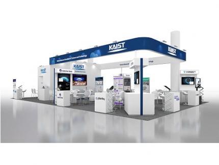
< Image 1. 3D-Graphical Profile of CES 2025 KAIST Exhibition Booth >
KAIST (President Kwang-Hyung Lee) announced on the 31st that it will operate a 140㎡ standalone booth at CES Eureka Park, which will be held in Las Vegas, USA from January 7th to 10th next year, to showcase KAIST's innovative technologies to global companies and investors.
KAIST startups VIRNECT, Standard Energy, A2US, and Panmnesia, Inc. won the 2025 CES Innovation Awards. ▴VIRNECT won the Innovation Award in the ‘Industrial Equipment and Machinery’ category for ‘VisionX’, an AI-based smart glass for industrial sites; ▴Standard Energy Co., Ltd. won the Innovation Award in the ‘Smart City’ category for developing the world’s first vanadium-ion battery; ▴A2US won the Innovation Award in the ‘Environment & Energy’ category for its portable air purifier that eliminates bacteria, odors, and fine dust in the air with just water droplets; ▴Panmnesia, Inc. won the Innovation Award in the ‘Computer Peripherals and Accessories’ category for its ‘CXL-based GPU Memory Expansion Kit’ that can drastically reduce the cost of building AI infrastructure.
< Image 2. (From left on the top row) VIRNECT, Standard Energy, (From left on the bottom row) A2US, Panmnesia, Inc. >
This exhibition will feature 15 startups that are standing out in cutting-edge technologies such as artificial intelligence (AI), robotics, mobility, and sustainability. In particular, AI-based deep tech startups in various industries such as logistics, architecture, and medicine will take up half of the total, showcasing the companies’ innovative AI technologies.
Polyphenol Factory Co.,Ltd introduces ‘Grabity’, a hair loss shampoo launched domestically, which applies the patented ingredient ‘LiftMax 308™’ that forms an instantaneous protective layer on the hair during the shampooing process. A real-time demonstration will be held at this exhibition hall so that visitors can experience the effects of the ingredient directly, and plans to enter the global market starting with the launch on Amazon in the US in January 2025.
VIRNECT will present ‘VisionX’, a prototype that won the Innovation Award this time. The product provides a chatbot AI through an AI voice interface, and has a function that allows users to check the status of the equipment in real time through conversations with the AI and receive troubleshooting guidance through voice conversations, so users can experience it directly at the KAIST Hall.
‘Standard Energy’ plans to exhibit ‘Energy Tile’, an indoor ESS that utilizes the world’s first vanadium ion battery (hereinafter referred to as VIB). VIB is absolutely safe from fire and has high installation flexibility, so it can be applied to smart cities and AI data centers.
‘A2US’ is the only company in the world that has hydroxyl radical water production technology, and won the Innovation Award for its first product, an air purifier. In the future, it is expected to be widely commercialized in air and water purification, smart farms, food tech, and semiconductor cleaning using safe and environmentally friendly hydroxyl radical water.
Panmnesia, Inc. won the CES Innovation Award for its GPU memory expansion solution equipped with its CXL 3.1 IP. By connecting a memory expansion device using Panmnesia’s CXL IP, the GPU’s memory capacity can be expanded to the terabyte level. Following the Innovation Award for ‘CXL-equipped AI Accelerator’ at CES 2024 last year, it is the only company to have won the Innovation Award for its AI-oriented CXL solution for two consecutive years.
In addition, technologies from a total of 15 companies will be introduced, including ▴Omelet ▴NEXTWAVE ▴Planby Technologies ▴Cosmo Bee ▴ImpactAI ▴Roen Surgical ▴DIDEN Roboticss ▴Autopedia ▴OAQ ▴HydroXpand ▴BOOKEND ▴Sterri.
On the central stage of the KAIST Hall, KAIST students selected as CES Student Supporters will conduct interviews with participating companies and promote the companies' innovative technologies and solutions. On the 8th, from 5 PM to 7 PM, a KAIST NIGHT event will be held where pre-invited investors and participating companies can network.
Keon Jae Lee, the head of the Institute of Technology Value Creation, said, “Through CES 2025, we will showcase innovative technologies and solutions from startups based on KAIST’s deep science and deep tech, and lead commercialization in cutting-edge technology fields such as AI, robotics, mobility, and environment/energy. KAIST plans to further promote technology commercialization by supporting the growth and marketing of innovative startups through the Institute of Technology Value Creation and by strengthening global networks and expanding cooperation opportunities.”
2024.12.31 View 7768
 -
 A KAIST Team Develops Face-Conforming LED Mask Showing 340% Improved Efficacy in Deep Skin Elasticity
- A KAIST research team led by Professor Keon Jae Lee has developed a deep skin-stimulating LED mask which has been verified in clinical trials to improve dermis elasticity by 340%.
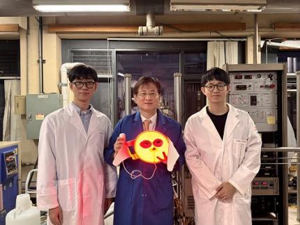
< Figure 1. Overall concept of face-fit surface-lighting micro-LEDs (FSLED) mask. a. Optical image of the FSLED mask showing uniform surface-lighting. schematic illustration of the FSLED mask. The 2D to 3D transformation procedure b. Difference in cosmetic effect on deep skin elasticity, wrinkles, and sagging between FSLED mask and CLED mask. (improvement percentage in eight weeks) >
Conventional LED masks, with their rigid design, fail to conform closely to the skin's contours. This limitation causes substantial light reflection, with up to 90% reflected over a distance of 2 cm, reducing light penetration and limiting stimulation of the deep skin layers essential for effective skin rejuvenation.
To address these challenges, Professor Lee's team developed a face-conforming surface lighting micro-LED (FSLED) mask, which can provide uniform photostimulation to the dermis. The key technology lies in the mask's ability to deliver uniform light to deep skin tissues while maintaining a conformal skin attachment. This is achieved through a 3D origami structure, integrated with 3,770 micro-LEDs and flexible surface light-diffusion layer, minimizing the gaps between the light source and the skin.
In clinical trials involving 33 participants, the FSLED mask demonstrated a 340% improvement in deep skin elasticity compared to conventional LED masks, proving its efficacy in significantly reducing skin wrinkles, sagging and aging.
Professor Keon Jae Lee said, “The FSLED mask provides cosmetic benefits to the entire facial dermis without the side effects of low-temperature burns, making home-care anti-aging treatment that enhances the quality of human life possible. The product is being manufactured by Fronics, KAIST startup company, and will be distributed globally through Amorepacific's network, with sales starting in November.”
This result titled “Clinical Validation of Face-fit Surface-lighting Micro Light-emitting Diode Mask for Skin Anti-aging Treatment”, in which Min Seo Kim, a student of the Master-Doctorate integrated program, and Jaehun An, a Ph.D. candidate, in the Department of Materials Science and Engineering of KAIST, took part as co-first authors, was published in Advanced Materials on October 22nd, 2024 (DOI: 10.1002/adma.202411651).
Introductory Video: Face-conforming surface LED mask for skin anti-aging ( https://www.youtube.com/watch?v=kSccLwx8N_w )
2024.10.29 View 8776
 -
 A KAIST Team Develops Selective Transfer Printing Technology for MicroLEDs
- A KAIST research team led by Professor Keon Jae Lee demonstrates the transfer printing of a large number of micro-sized inorganic semiconductor chips via the selective modulation of micro-vacuum force.
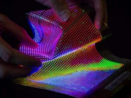
MicroLEDs are a light source for next-generation displays that utilize inorganic LED chips with a size of less than 100 μm. MicroLEDs have attracted a great deal of attention due to their superior electrical/optical properties, reliability, and stability compared to conventional displays such as LCD, OLED, and QD. To commercialize microLEDs, transfer printing technology is essential for rearranging microLED dies from a growth substrate onto the final substrate with a desired layout and precise alignment. However, previous transfer methods still have many challenges such as the need for additional adhesives, misalignment, low transfer yield, and chip damage.
Professor Lee’s research team has developed a micro-vacuum assisted selective transfer printing (µVAST) technology to transfer a large number of microLED chips by adjusting the micro-vacuum suction force.
The key technology relies on a laser-induced etching (LIE) method for forming 20 μm-sized micro-hole arrays with a high aspect ratio on glass substrates at fabrication speed of up to 7,000 holes per second. The LIE-drilled glass is connected to the vacuum channels, controlling the micro-vacuum force at desired hole arrays to selectively pick up and release the microLEDs. The micro-vacuum assisted transfer printing accomplishes a higher adhesion switchability compared to previous transfer methods, enabling the assembly of micro-sized semiconductors with various heterogeneous materials, sizes, shapes, and thicknesses onto arbitrary substrates with high transfer yields.
< Figure 01. Concept of micro-vacuum assisted selective transfer printing (μVAST). >
Professor Keon Jae Lee said, “The micro-vacuum assisted transfer provides an interesting tool for large-scale, selective integration of microscale high-performance inorganic semiconductors. Currently, we are investigating the transfer printing of commercial microLED chips with an ejector system for commercializing next-generation displays (Large screen TVs, flexible/stretchable devices) and wearable phototherapy patches.”
This result titled “Universal selective transfer printing via micro-vacuum force” was published in Nature Communications on November 26th, 2023. (DOI: 10.1038/S41467-023-43342-8)
< Figure 02. Universal transfer printing of thin-film semiconductors via μVAST. >
< Figure 03. Flexible devices fabricated by μVAST. >
Title: Entire process including LIE and µVAST
Vimeo link: https://vimeo.com/894430416?share=copy
2023.12.19 View 5132
 -
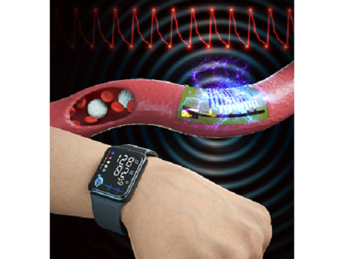 KAIST Team Develops Highly-Sensitive Wearable Piezoelectric Blood Pressure Sensor for Continuous Health Monitoring
- A collaborative research team led by KAIST Professor Keon Jae Lee verifies the accuracy of the highly-sensitive sensor through clinical trials
- Commercialization of the watch and patch-type sensor is in progress
A KAIST research team led by Professor Keon Jae Lee from the Department of Materials Science and Engineering and the College of Medicine of the Catholic University of Korea has developed a highly sensitive, wearable piezoelectric blood pressure sensor.
Blood pressure is a critical indicator for assessing general health and predicting stroke or heart failure. In particular, cardiovascular disease is the leading cause of global death, therefore, periodic measurement of blood pressure is crucial for personal healthcare.
Recently, there has been a growing interest in healthcare devices for continuous blood pressure monitoring. Although smart watches using LED-based photoplethysmography (PPG) technology have been on market, these devices have been limited by the accuracy constraints of optical sensors, making it hard to meet the international standards of automatic sphygmomanometers.
Professor Lee’s team has developed the wearable piezoelectric blood pressure sensor by transferring a highly sensitive, inorganic piezoelectric membrane from bulk sapphire substrates to flexible substrates. Ultrathin piezoelectric sensors with a thickness of several micrometers (one hundredth of the human hair) exhibit conformal contact with the skin to successfully collect accurate blood pressure from the subtle pulsation of the blood vessels.
Clinical trial at the St. Mary’s Hospital of the Catholic University validated the accuracy of blood pressure sensor at par with international standard with errors within ±5 mmHg and a standard deviation under 8 mmHg for both systolic and diastolic blood pressure. In addition, the research team successfully embedded the sensor on a watch-type product to enable continuous monitoring of blood pressure.
Prof. Keon Jae Lee said, “Major target of our healthcare devices is hypertensive patients for their daily medical check-up. We plan to develop a comfortable patch-type sensor to monitor blood pressure during sleep and have a start-up company commercialize these watch and patch-type products soon.”
This result titled “Clinical validation of wearable piezoelectric blood pressure sensor for health monitoring” was published in the online issue of Advanced Materials on March 24th, 2023. (DOI: 10.1002/adma.202301627)
Figure 1. Schematic illustration of the overall concept for a wearable piezoelectric blood pressure sensor (WPBPS).
Figure 2. Wearable piezoelectric blood pressure sensor (WPBPS) mounted on a watch (a) Schematic design of the WPBPS-embedded wristwatch. (b) Block diagram of the wireless communication circuit, which filters, amplifies, and transmits wireless data to portable devices. (c) Pulse waveforms transmitted from the wristwatch to the portable device by the wireless communication circuit. The inset shows a photograph of monitoring a user’s beat-to-beat pulses and their corresponding BP values in real time using the developed WPBPS-mounted wristwatch.
2023.04.17 View 10634
 -
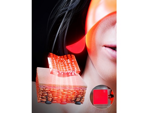 KAIST Team Develops Surface-Lighting MicroLED Patch with Significant Melanogenesis Inhibition Effect
A KAIST research team led by Ph.d candidate Jae Hee Lee and Professor Keon Jae Lee from the Department of Materials Science and Engineering has developed a surface-lighting microLED patch for UV-induced melanogenesis inhibition.
Melanin is brown or dark pigments existing in the skin, which can be abnormally synthesized by external UV or stress. Since the excessive melanin leads to skin diseases such as spots and freckles, proper treatment is required to return normal skin condition.
Recently, LED-based photo-stimulators have been released for skin care, however, their therapeutic effect is still controversial. Since conventional LED stimulators cannot conformally attach to the human skin, distance-induced side effects are caused by light loss and high heat transfer. To achieve effective phototreatment, the LED stimulator needs to be irradiated in contact with the human skin surface, enabling proper and uniform light deliver to the dermis with minimal optical loss.
In this work, the research team fabricated skin-attachable surface-lighting microLED (SµLED, 4 × 4 cm2) patch by utilizing a thousand of microLED chips and silica-embedded light diffusion layer. 100 µm-sized LED chips are vertically-interconnected for high flexibility and low heat generation, allowing its long-term operation on the human skin.
< Image 1. The overall concept of SµLED patch. a) SµLED patch operated on the human skin. b) Schematic illustration of SµLED patch structure. c) 4 × 4 cm2-sized SµLED patch. d) Schematic illustration of the advantages of SµLED patch such as efficient light delivery, low heat generation, and surface-lighting irradiation. >
The research team confirmed melanogenesis inhibition by irradiating the SµLED patch and the conventional LED (CLED) on the artificial human skin and mice dorsal skin. The SµLED-treated groups of human cells and mouse tissues showed minimal epidermal photo-toxicity and consistently effective reduction in synthesized melanin, compared to CLED-treated groups. In addition, significant suppression of proteins/catalysts expression involved in melanin synthesis such as MITF (microphthalmia-associated transcription factor), Melan-A and tyrosinase was verified.
< Image 2. The efficacy of melanogenesis inhibition on 3D human skin cells. a). Different irradiation conditions for a-MSH (major factor to stimulate melanin synthesis) treated cells. b) The ratio of pigmented area to total epidermis area. c) Relative variance of melanin level in 1 cm2-sized skin cells. A low variance means that melanin is evenly distributed, and a high variance means that the melanin is irregularly distributed. d) Optical images after in vitro experiments for 12 days. Scale bar, 1cm. e) Histological analysis of 3D skin, showing the greatest reduction in melanin after SµLED irradiation. Scale bar, 20 µm. >
< Image 3. The efficacy of melanogenesis inhibition on mouse dorsal skin. a) Optical images of mice dorsal skin after photo-treatment for 20 days. b) Histological analysis of mice dorsal skin. Less brown color means less expression of protein/catalysis involved in melanin synthesis. Scale bar, 50 µm. >
Prof. Keon Jae Lee said, “Our inorganic-based SµLED patch has outstanding characteristics in light efficiency, reliability, and durability. The SµLED patch is expected to give a great impact on the cosmetic field by reducing side effects and maximizing phototherapeutic effects.” The core technology of cosmetic SµLED has been transferred to Fronics co., Ltd, founded by Prof. Lee. Fronics is building foundry and equipment for mass production of SµLED masks for whole face cover and plans to release the products in March next year.
This paper entitled “Wearable Surface-Lighting Micro-Light-Emitting Diode Patch for Melanogenesis Inhibition” was published in the November 2022 issue of Advanced Healthcare Materials.
2022.11.22 View 14267
 -
 Neuromorphic Memory Device Simulates Neurons and Synapses
Simultaneous emulation of neuronal and synaptic properties promotes the development of brain-like artificial intelligence
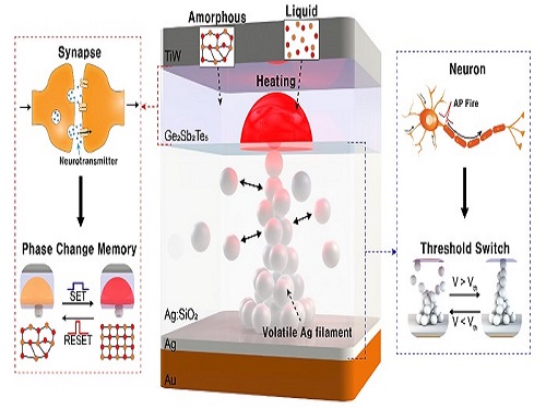
Researchers have reported a nano-sized neuromorphic memory device that emulates neurons and synapses simultaneously in a unit cell, another step toward completing the goal of neuromorphic computing designed to rigorously mimic the human brain with semiconductor devices.
Neuromorphic computing aims to realize artificial intelligence (AI) by mimicking the mechanisms of neurons and synapses that make up the human brain. Inspired by the cognitive functions of the human brain that current computers cannot provide, neuromorphic devices have been widely investigated. However, current Complementary Metal-Oxide Semiconductor (CMOS)-based neuromorphic circuits simply connect artificial neurons and synapses without synergistic interactions, and the concomitant implementation of neurons and synapses still remains a challenge. To address these issues, a research team led by Professor Keon Jae Lee from the Department of Materials Science and Engineering implemented the biological working mechanisms of humans by introducing the neuron-synapse interactions in a single memory cell, rather than the conventional approach of electrically connecting artificial neuronal and synaptic devices.
Similar to commercial graphics cards, the artificial synaptic devices previously studied often used to accelerate parallel computations, which shows clear differences from the operational mechanisms of the human brain. The research team implemented the synergistic interactions between neurons and synapses in the neuromorphic memory device, emulating the mechanisms of the biological neural network. In addition, the developed neuromorphic device can replace complex CMOS neuron circuits with a single device, providing high scalability and cost efficiency.
The human brain consists of a complex network of 100 billion neurons and 100 trillion synapses. The functions and structures of neurons and synapses can flexibly change according to the external stimuli, adapting to the surrounding environment. The research team developed a neuromorphic device in which short-term and long-term memories coexist using volatile and non-volatile memory devices that mimic the characteristics of neurons and synapses, respectively. A threshold switch device is used as volatile memory and phase-change memory is used as a non-volatile device. Two thin-film devices are integrated without intermediate electrodes, implementing the functional adaptability of neurons and synapses in the neuromorphic memory.
Professor Keon Jae Lee explained, "Neurons and synapses interact with each other to establish cognitive functions such as memory and learning, so simulating both is an essential element for brain-inspired artificial intelligence. The developed neuromorphic memory device also mimics the retraining effect that allows quick learning of the forgotten information by implementing a positive feedback effect between neurons and synapses.”
This result entitled “Simultaneous emulation of synaptic and intrinsic plasticity using a memristive synapse” was published in the May 19, 2022 issue of Nature Communications.
-Publication:Sang Hyun Sung, Tae Jin Kim, Hyera Shin, Tae Hong Im, and Keon Jae Lee (2022) “Simultaneous emulation of synaptic and intrinsic plasticity using a memristive synapse,” Nature Communications May 19, 2022 (DOI: 10.1038/s41467-022-30432-2)
-Profile:Professor Keon Jae Leehttp://fand.kaist.ac.kr
Department of Materials Science and EngineeringKAIST
2022.05.20 View 16298
 -
 Biomimetic Resonant Acoustic Sensor Detecting Far-Distant Voices Accurately to Hit the Market
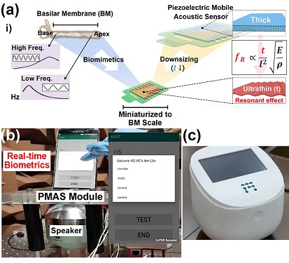
A KAIST research team led by Professor Keon Jae Lee from the Department of Materials Science and Engineering has developed a bioinspired flexible piezoelectric acoustic sensor with multi-resonant ultrathin piezoelectric membrane mimicking the basilar membrane of the human cochlea. The flexible acoustic sensor has been miniaturized for embedding into smartphones and the first commercial prototype is ready for accurate and far-distant voice detection.
In 2018, Professor Lee presented the first concept of a flexible piezoelectric acoustic sensor, inspired by the fact that humans can accurately detect far-distant voices using a multi-resonant trapezoidal membrane with 20,000 hair cells. However, previous acoustic sensors could not be integrated into commercial products like smartphones and AI speakers due to their large device size.
In this work, the research team fabricated a mobile-sized acoustic sensor by adopting ultrathin piezoelectric membranes with high sensitivity. Simulation studies proved that the ultrathin polymer underneath inorganic piezoelectric thin film can broaden the resonant bandwidth to cover the entire voice frequency range using seven channels. Based on this theory, the research team successfully demonstrated the miniaturized acoustic sensor mounted in commercial smartphones and AI speakers for machine learning-based biometric authentication and voice processing. (Please refer to the explanatory movie KAIST Flexible Piezoelectric Mobile Acoustic Sensor).
The resonant mobile acoustic sensor has superior sensitivity and multi-channel signals compared to conventional condenser microphones with a single channel, and it has shown highly accurate and far-distant speaker identification with a small amount of voice training data. The error rate of speaker identification was significantly reduced by 56% (with 150 training datasets) and 75% (with 2,800 training datasets) compared to that of a MEMS condenser device.
Professor Lee said, “Recently, Google has been targeting the ‘Wolverine Project’ on far-distant voice separation from multi-users for next-generation AI user interfaces. I expect that our multi-channel resonant acoustic sensor with abundant voice information is the best fit for this application. Currently, the mass production process is on the verge of completion, so we hope that this will be used in our daily lives very soon.”
Professor Lee also established a startup company called Fronics Inc., located both in Korea and U.S. (branch office) to commercialize this flexible acoustic sensor and is seeking collaborations with global AI companies.
These research results entitled “Biomimetic and Flexible Piezoelectric Mobile Acoustic Sensors with Multi-Resonant Ultrathin Structures for Machine Learning Biometrics” were published in Science Advances in 2021 (7, eabe5683).
-Publication
“Biomimetic and flexible piezoelectric mobile acoustic sensors with multiresonant ultrathin structures for machine learning biometrics,” Science Advances (DOI: 10.1126/sciadv.abe5683)
-Profile
Professor Keon Jae Lee
Department of Materials Science and Engineering
Flexible and Nanobio Device Lab
http://fand.kaist.ac.kr/
KAIST
2021.06.14 View 11684
 -
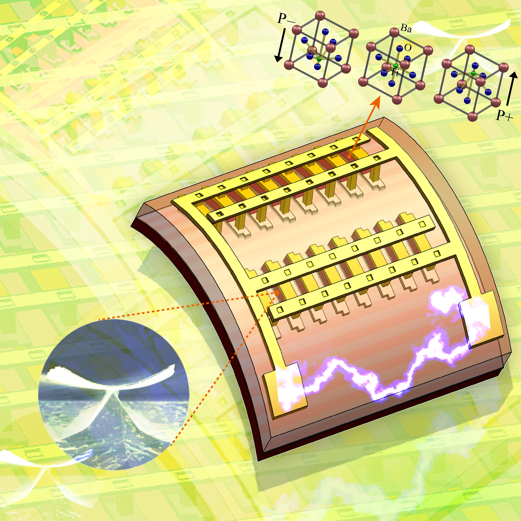 The KAIST & GIT team developed a power generation technology using bendable thin film nano-materials.
Figure description: Flexible thin film nanomaterials produce electricity.
Can a heart implanted micro robot operate permanently?
Can cell phones and tiny robots implanted in the heart operate permanently without having their batteries charged?
It might sound like science fiction, but these things seem to be possible in the near future. The team of Prof. Keon Jae Lee (KAIST, Dept. of Materials Science and Engineering) and Prof. Zhong Lin Wang (Georgia Institute of Technology, Dept. of Materials Science and Engineering) has developed new forms of highly efficient, flexible nanogenerator technology using the freely bendable piezoelectric ceramic thin film nano-materials that can convert tiny movements of the human body (such as heart beats and blood flow) into electrical energy.
The piezoelectric effect refers to voltage generation when pressure or bending strength is applied to piezoelectric materials. The ceramics, containing a perovskite structure, have a high piezoelectric efficiency. Until now, it has been very difficult to use these ceramic materials to fabricate flexible electronic systems due to their brittle property.
The research team, however, has succeeded in developing a bio-eco-friendly ceramic thin film nanogenerator that is freely bendable without breakdown.
Nanogenerator technology, a power generating system without wires or batteries, combines nanotechnology with piezoelectrics that can be used not only in personal mobile electronics but also in bio-implantable sensors or as an energy source for micro robots. Energy sources in nature (wind, vibration, and sound) and biomechanical forces produced by the human body (heart beats, blood flow, and muscle contraction/relaxation) can infinitely produce nonpolluting energy. (Nanogenerator produces electricity by external forces: http://www.youtube.com/watch?v=tvj0SsBqpBw)
Prof. Keon Jae Lee (KAIST) was involved in the first co-invention of “High Performance Flexible Single Crystal Electronics” during his PhD course at the University of Illinois at Urbana-Champaign. This nanogenerator technology, based on the previous invention, utilized the similar protocol of transferring ceramic thin film nano-materials on flexible substrates and produced voltage generation between electrodes.
Prof. Zhong Lin Wang (Georgia Tech, inventor of the nanogenerator) said, “This technology can be used to turn on an LED by slightly modifying circuits and operate touchable flexible displays. In addition, thin film nano-materials (‘barium titanate’) of this research have the property of both high efficiency and lead-free bio compatibility, which can be used in future medical applications.” This result is published in November online issue of ‘Nano Letters’ ACS journal.
<Video>
Youtube link: http://www.youtube.com/watch?v=tvj0SsBqpBw
Thin Film Nanogenerator produces electricity by external forces.
2010.11.23 View 18132