Packaging
-
 Scientists Discover the Mechanism of DNA High-Order Structure Formation
(Molecular structures of Abo1 in different energy states (left), Demonstration of an Abo1-assisted histone loading onto DNA by the DNA curtain assay. )
The genetic material of our cells—DNA—exists in a high-order structure called “chromatin”. Chromatin consists of DNA wrapped around histone proteins and efficiently packs DNA into a small volume. Moreover, using a spool and thread analogy, chromatin allows DNA to be locally wound or unwound, thus enabling genes to be enclosed or exposed. The misregulation of chromatin structures results in aberrant gene expression and can ultimately lead to developmental disorders or cancers. Despite the importance of DNA high-order structures, the complexity of the underlying machinery has circumvented molecular dissection.
For the first time, molecular biologists have uncovered how one particular mechanism uses energy to ensure proper histone placement onto DNA to form chromatin. They published their results on Dec. 17 in Nature Communications.
The study focused on proteins called histone chaperones. Histone chaperones are responsible for adding and removing specific histones at specific times during the DNA packaging process. The wrong histone at the wrong time and place could result in the misregulation of gene expression or aberrant DNA replication. Thus, histone chaperones are key players in the assembly and disassembly of chromatin.
“In order to carefully control the assembly and disassembly of chromatin units, histone chaperones act as molecular escorts that prevent histone aggregation and undesired interactions,” said Professor Ji-Joon Song in the Department of Biological Sciences at KAIST. “We set out to understand how a unique histone chaperone uses chemical energy to assemble or disassemble chromatin.”
Song and his team looked to Abo1, the only known histone chaperone that utilizes cellular energy (ATP). While Abo1 is found in yeast, it has an analogous partner in other organisms, including humans, called ATAD2. Both use ATP, which is produced through a cellular process where enzymes break down a molecule’s phosphate bond. ATP energy is typically used to power other cellular processes, but it is a rare partner for histone chaperones.
“This was an interesting problem in the field because all other histone chaperones studied to date do not use ATP,” Song said.
By imaging Abo1 with a single-molecule fluorescence imaging technique known as the DNA curtain assay, the researchers could examine the protein interactions at the single-molecule level. The technique allows scientists to arrange the DNA molecules and proteins on a single layer of a microfluidic chamber and examine the layer with fluorescence microscopy.
The researchers found through real-time observation that Abo1 is ring-shaped and changes its structure to accommodate a specific histone and deposit it on DNA. Moreover, they found that the accommodating structural changes are powered by ADP.
“We discovered a mechanism by which Abo1 accommodates histone substrates, ultimately allowing it to function as a unique energy-dependent histone chaperone,” Song said. “We also found that despite looking like a protein disassembly machine, Abo1 actually loads histone substrates onto DNA to facilitate chromatin assembly.”
The researchers plan to continue exploring how energy-dependent histone chaperones bind and release histones, with the ultimate goal of developing therapeutics that can target cancer-causing misbehavior by Abo1’s analogous human counterpart, ATAD2.
-Profile
Professor Ji-Joon Song
Department of Biological Sciences KI for the BioCentury (https://kis.kaist.ac.kr/index.php?mid=KIB_O) KAIST
2020.01.07 View 11023
 -
 Tae-Wan Kim, a doctoral candidate, receives the best paper award from ECTC
The 2014 Electronic Components and Technology Conference (ECTC) will take place on May 27-30 in Florida, USA. Tae-Wan Kim, a Ph.D. candidate at the Department of Materials Science Engineering (MSE), KAIST, will receive the Intel Best Student Paper Award at the conference.ECTC is the premier international conference that brings together the best researchers and engineers in packaging, components and microelectronic systems science, technology and education in an environment of cooperation and technical exchange. The conference is sponsored by the Components, Packaging and Manufacturing Technology (CPMT) Society of IEEE (Institute of Electrical and Electronics Engineering).The paper describes research on novel nanofiber anisotropic conductive films for ultra fine pitch electronic package application, which was written under the guidance of Professor Kyung-Wook Paik of the MSE Department. In the past ten years, two of his students have received the best paper award from ECTC.
2014.03.14 View 12384
 -
 Inexpensive Separation Method of Graphene Developed
The problem with commercializing graphene that is synthesized onto metals over a wide area is that it can not be separated from the metal. However, a groundbreaking separation technology which is both cheap and environment friendly has been developed.
Prof. Taek soo Kim and Prof. Byung Jin Cho"s research teams have conducted this research under the support of the Global Frontier program and Researcher Support Program initiated by The Ministry of Education and Science and Korea Research Foundation. The research results have been posted on the online news flash of Nano Letters on februrary 29th. (Thesis title: Direct Measurement of Adhesion Energy of Monolayer Graphene As-Grown on Copper and Its Application to Renewable Transfer Process)
The research has generated exact results on the interfacial adhesive energy of graphene and its surface material for the first time. Through this, the catalyst metal are no longer to be used just once, but will be used for an infinite number of times, thereby being ecofriendly and efficient.
Wide area graphine synthesized onto the catalyst meatal are used in various ways such as for display and for solar cells. There has been much research going on in this field. However, in order to use this wide area graphene, the graphene must be removed from the catalyst metal without damage.
Until now, the metal had been melted away through the use of chemical substances in order to separate the graphene. However, this method has been very problematic. The metal can not be reused, the costs are very high, much harmful wastes were created in the process of melting the metals, and the process was very complicated.
The research teams of Professors Taek Su Kim and Byung Jin Cho measured the interfacial adhesive energy of the synthesized graphene and learned that it could be easily removed.
Also, the mechanically removed graphene was successfully used in creating molecular electronic devices directly. This has thus innovatively shortened the graphene manufacturing process. Also, it has been confirmed that the metalic board can be reused multiple times after the graphene is removed. A new, ecofriendly and cost friendly method of graphene manufacturing has been paved.
Through this discovery, it is expected that graphene will become easier to manufacture and that the period til the commercialization date of graphene will therefore be greatly reduced
Prof. Cho stated " This reserach has much academical meaning significance in that it has successfully defined the surfacial adhesive energy between the graphene and its catalyst material and it should receive much attention in that it solved the largest technical problem involved in the production of graphene.
2012.04.04 View 15099
 -
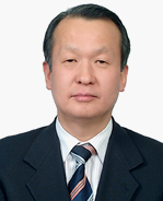 Prof. Yu Wins Sidney Stein International Award
Prof. Jin Yu of the Department of Materials Science and Engineering won the Sidney J. Stein International Award at the plenary session of the International Microelectronics and Packaging Society (IMAPS) held in San Jose, the United States, on Nov. 3.
The Sidney Stein International Award recognizes an individual who is regarded as providing significant international technical and/or leadership contributions to the microelectronics packaging industry, while participating and demonstrating support of IMAPS international activities to enhance the electronics packaging profession.
The International Microelectronics And Packaging Society is the largest society dedicated to the advancement and growth of microelectronics and electronics packaging. It offers chapters around the globe, creating global networks of more than 4,000 members in the United States and an additional 4,000 members throughout Europe and Asia. Prof. Yu currently serves as the chairman of its Asia League Chapter and the Korean Microelectronics and Packaging Society.
2009.11.20 View 13675
 -
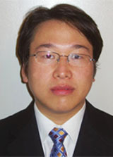 KAIST Graduate Selected As Winner of IEEE Outstanding Young Engineer Award
- First Korean winner of IEEE Outstanding Young Engineer Award
Dr. Myung-Jin Rhim, Bachelor, Master, and Ph.D of KAIST, has been selected to receive 2007 Outstanding Young Engineer Award by the Institute of Electrical and Electronics Engineers (IEEE) Components, Packaging, and Manufacturing Technology (CPMT) Society. Dr. Rhim will be the first Korean winner of the award.
Dr. Rhim received his Ph.D of Materials Science & Engineering at KAIST in 2001 and has made outstanding research outputs, such as 28 papers at international journals covered by Science Citation Index (SCI) and 12 international patents. He has been also listed in Marquis Who’s Who in the World, Who’s Who of Emerging Leaders, Who’s Who in Asia, and Outstanding Intellectual of the 21st Century, 21st Century Award for Achievement published by the International Biographical Centre of Cambridge, England.
IEEE CPMT Society has yearly awarded the Outstanding Young Engineer Award to a scientist or engineer of electronic components, packaging, and manufacturing technology prior to his or her 35th birthday in recognition of his or her research achievements. Dr. Rhim is now in his postdoctoral program at Georgia Institute of Technology in USA.
2007.06.14 View 17784
 -
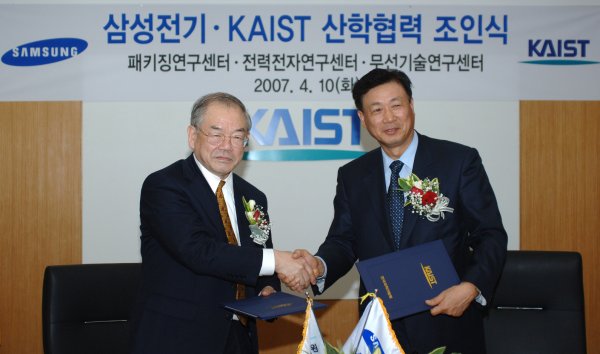 KAIST and Samsung Electrics Signs Cooperation Agreement
- Industry-Academy cooperation program for enhancing global competitiveness and for obtaining new growth momentum
- Two research institutes - Power Electronics Institute and Packaging Institute - open in KAIST- Fostering customized experts through researcher reeducation, field experiences, etc.
KAIST (President Nam-Pyo Suh) and Samsung Electronics (President Ho-Moon Kang) will be promoting industry-academy cooperative activities to enhance their global competitiveness and to obtain new growth momentum.
The both parties singed the agreement at KAIST conference room 1 on April 10, Tuesday, and two new research institutes - Power Electronics Institute (PEI) and Packaging Institute (PI) -opened this day. As a result, KAIST holds three research institutes managed in cooperation with Samsung Electronics, including the Radio Technology Institute (RTI) which was opened in 2005.
The PEI aims to develop power supply devices for high-efficiency and high-power servers of flat display power supply, and will foster customized experts through researcher reeducation and field experiences.
The PI will foster experts for improving packaging qualities and for developing next-generation technologies. Packing technologies are in the core field of electronics part industries which is going for integrating, systemizing and modulization.
“I’m sure outstanding industry-academy researches and student education will raise the standings of the both bodies, and I promise generous support to produce further significant research results,” said KAIST President Suh.
“This cooperation program will become an example of successful industry-academy cooperation. I’m expecting KAIST will become a trustworthy partner for Samsung Electronics to jump into one of the world’s top-class enterprises,” said Samsung Electronics President Kang.
2007.04.23 View 14565