Yongsoo+Yang
-
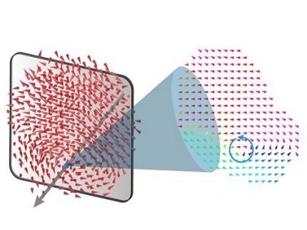 A 20-year-old puzzle solved: KAIST research team reveals the 'three-dimensional vortex' of zero-dimensional ferroelectrics
Materials that can maintain a magnetized state by themselves without an external magnetic field (i.e., permanent magnets) are called ferromagnets. Ferroelectrics can be thought of as the electric counterpart to ferromagnets, as they maintain a polarized state without an external electric field. It is well-known that ferromagnets lose their magnetic properties when reduced to nano sizes below a certain threshold. What happens when ferroelectrics are similarly made extremely small in all directions (i.e., into a zero-dimensional structure such as nanoparticles) has been a topic of controversy for a long time.
< (From left) Professor Yongsoo Yang, the corresponding author, and Chaehwa Jeong, the first author studying in the integrated master’s and doctoral program, of the KAIST Department of Physics >
The research team led by Dr. Yongsoo Yang from the Department of Physics at KAIST has, for the first time, experimentally clarified the three-dimensional, vortex-shaped polarization distribution inside ferroelectric nanoparticles through international collaborative research with POSTECH, SNU, KBSI, LBNL and University of Arkansas.
About 20 years ago, Prof. Laurent Bellaiche (currently at University of Arkansas) and his colleagues theoretically predicted that a unique form of polarization distribution, arranged in a toroidal vortex shape, could occur inside ferroelectric nanodots. They also suggested that if this vortex distribution could be properly controlled, it could be applied to ultra-high-density memory devices with capacities over 10,000 times greater than existing ones. However, experimental clarification had not been achieved due to the difficulty of measuring the three-dimensional polarization distribution within ferroelectric nanostructures.
The research team at KAIST successfully solved this 20-year-old challenge by implementing a technique called atomic electron tomography. This technique works by acquiring atomic-resolution transmission electron microscope images of the nanomaterials from multiple tilt angles, and then reconstructing them back into three-dimensional structures using advanced reconstruction algorithms. Electron tomography can be understood as essentially the same method with the CT scans used in hospitals to view internal organs in three dimensions; the KAIST team adapted it uniquely for nanomaterials, utilizing an electron microscope at the single-atom level.
< Figure 1. Three-dimensional polarization distribution of BaTiO3 nanoparticles revealed by atomic electron tomography. >(Left) Schematic of the electron tomography technique, which involves acquiring transmission electron microscope images at multiple tilt angles and reconstructing them into 3D atomic structures.(Center) Experimentally determined three-dimensional polarization distribution inside a BaTiO3 nanoparticle via atomic electron tomography. A vortex-like structure is clearly visible near the bottom (blue dot).(Right) A two-dimensional cross-section of the polarization distribution, thinly sliced at the center of the vortex, with the color and arrows together indicating the direction of the polarization. A distinct vortex structure can be observed.
Using atomic electron tomography, the team completely measured the positions of cation atoms inside barium titanate (BaTiO3) nanoparticles, a well-known ferroelectric material, in three dimensions. From the precisely determined 3D atomic arrangements, they were able to further calculate the internal three-dimensional polarization distribution at the single-atom level. The analysis of the polarization distribution revealed, for the first time experimentally, that topological polarization orderings including vortices, anti-vortices, skyrmions, and a Bloch point occur inside the 0-dimensional ferroelectrics, as theoretically predicted 20 years ago. Furthermore, it was also found that the number of internal vortices can be controlled depending on their sizes.
Prof. Sergey Prosandeev and Prof. Bellaiche (who proposed with other co-workers the polar vortex ordering theoretically 20 years ago), joined this collaboration and further proved that the vortex distribution results obtained from experiments are consistent with theoretical calculations.
By controlling the number and orientation of these polarization distributions, it is expected that this can be utilized into next-generation high-density memory device that can store more than 10,000 times the amount of information in the same-sized device compared to existing ones.
Dr. Yang, who led the research, explained the significance of the results: “This result suggests that controlling the size and shape of ferroelectrics alone, without needing to tune the substrate or surrounding environmental effects such as epitaxial strain, can manipulate ferroelectric vortices or other topological orderings at the nano-scale. Further research could then be applied to the development of next-generation ultra-high-density memory.”
This research, with Chaehwa Jeong from the Department of Physics at KAIST as the first author, was published online in Nature Communications on May 8th (Title: Revealing the Three-Dimensional Arrangement of Polar Topology in Nanoparticles).
The study was mainly supported by the National Research Foundation of Korea (NRF) Grants funded by the Korean Government (MSIT).
2024.05.31 View 7697
A 20-year-old puzzle solved: KAIST research team reveals the 'three-dimensional vortex' of zero-dimensional ferroelectrics
Materials that can maintain a magnetized state by themselves without an external magnetic field (i.e., permanent magnets) are called ferromagnets. Ferroelectrics can be thought of as the electric counterpart to ferromagnets, as they maintain a polarized state without an external electric field. It is well-known that ferromagnets lose their magnetic properties when reduced to nano sizes below a certain threshold. What happens when ferroelectrics are similarly made extremely small in all directions (i.e., into a zero-dimensional structure such as nanoparticles) has been a topic of controversy for a long time.
< (From left) Professor Yongsoo Yang, the corresponding author, and Chaehwa Jeong, the first author studying in the integrated master’s and doctoral program, of the KAIST Department of Physics >
The research team led by Dr. Yongsoo Yang from the Department of Physics at KAIST has, for the first time, experimentally clarified the three-dimensional, vortex-shaped polarization distribution inside ferroelectric nanoparticles through international collaborative research with POSTECH, SNU, KBSI, LBNL and University of Arkansas.
About 20 years ago, Prof. Laurent Bellaiche (currently at University of Arkansas) and his colleagues theoretically predicted that a unique form of polarization distribution, arranged in a toroidal vortex shape, could occur inside ferroelectric nanodots. They also suggested that if this vortex distribution could be properly controlled, it could be applied to ultra-high-density memory devices with capacities over 10,000 times greater than existing ones. However, experimental clarification had not been achieved due to the difficulty of measuring the three-dimensional polarization distribution within ferroelectric nanostructures.
The research team at KAIST successfully solved this 20-year-old challenge by implementing a technique called atomic electron tomography. This technique works by acquiring atomic-resolution transmission electron microscope images of the nanomaterials from multiple tilt angles, and then reconstructing them back into three-dimensional structures using advanced reconstruction algorithms. Electron tomography can be understood as essentially the same method with the CT scans used in hospitals to view internal organs in three dimensions; the KAIST team adapted it uniquely for nanomaterials, utilizing an electron microscope at the single-atom level.
< Figure 1. Three-dimensional polarization distribution of BaTiO3 nanoparticles revealed by atomic electron tomography. >(Left) Schematic of the electron tomography technique, which involves acquiring transmission electron microscope images at multiple tilt angles and reconstructing them into 3D atomic structures.(Center) Experimentally determined three-dimensional polarization distribution inside a BaTiO3 nanoparticle via atomic electron tomography. A vortex-like structure is clearly visible near the bottom (blue dot).(Right) A two-dimensional cross-section of the polarization distribution, thinly sliced at the center of the vortex, with the color and arrows together indicating the direction of the polarization. A distinct vortex structure can be observed.
Using atomic electron tomography, the team completely measured the positions of cation atoms inside barium titanate (BaTiO3) nanoparticles, a well-known ferroelectric material, in three dimensions. From the precisely determined 3D atomic arrangements, they were able to further calculate the internal three-dimensional polarization distribution at the single-atom level. The analysis of the polarization distribution revealed, for the first time experimentally, that topological polarization orderings including vortices, anti-vortices, skyrmions, and a Bloch point occur inside the 0-dimensional ferroelectrics, as theoretically predicted 20 years ago. Furthermore, it was also found that the number of internal vortices can be controlled depending on their sizes.
Prof. Sergey Prosandeev and Prof. Bellaiche (who proposed with other co-workers the polar vortex ordering theoretically 20 years ago), joined this collaboration and further proved that the vortex distribution results obtained from experiments are consistent with theoretical calculations.
By controlling the number and orientation of these polarization distributions, it is expected that this can be utilized into next-generation high-density memory device that can store more than 10,000 times the amount of information in the same-sized device compared to existing ones.
Dr. Yang, who led the research, explained the significance of the results: “This result suggests that controlling the size and shape of ferroelectrics alone, without needing to tune the substrate or surrounding environmental effects such as epitaxial strain, can manipulate ferroelectric vortices or other topological orderings at the nano-scale. Further research could then be applied to the development of next-generation ultra-high-density memory.”
This research, with Chaehwa Jeong from the Department of Physics at KAIST as the first author, was published online in Nature Communications on May 8th (Title: Revealing the Three-Dimensional Arrangement of Polar Topology in Nanoparticles).
The study was mainly supported by the National Research Foundation of Korea (NRF) Grants funded by the Korean Government (MSIT).
2024.05.31 View 7697 -
 Observing Individual Atoms in 3D Nanomaterials and Their Surfaces
Atoms are the basic building blocks for all materials. To tailor functional properties, it is essential to accurately determine their atomic structures. KAIST researchers observed the 3D atomic structure of a nanoparticle at the atom level via neural network-assisted atomic electron tomography.
Using a platinum nanoparticle as a model system, a research team led by Professor Yongsoo Yang demonstrated that an atomicity-based deep learning approach can reliably identify the 3D surface atomic structure with a precision of 15 picometers (only about 1/3 of a hydrogen atom’s radius). The atomic displacement, strain, and facet analysis revealed that the surface atomic structure and strain are related to both the shape of the nanoparticle and the particle-substrate interface.
Combined with quantum mechanical calculations such as density functional theory, the ability to precisely identify surface atomic structure will serve as a powerful key for understanding catalytic performance and oxidation effect.
“We solved the problem of determining the 3D surface atomic structure of nanomaterials in a reliable manner. It has been difficult to accurately measure the surface atomic structures due to the ‘missing wedge problem’ in electron tomography, which arises from geometrical limitations, allowing only part of a full tomographic angular range to be measured. We resolved the problem using a deep learning-based approach,” explained Professor Yang.
The missing wedge problem results in elongation and ringing artifacts, negatively affecting the accuracy of the atomic structure determined from the tomogram, especially for identifying the surface structures. The missing wedge problem has been the main roadblock for the precise determination of the 3D surface atomic structures of nanomaterials.
The team used atomic electron tomography (AET), which is basically a very high-resolution CT scan for nanomaterials using transmission electron microscopes. AET allows individual atom level 3D atomic structural determination.
“The main idea behind this deep learning-based approach is atomicity—the fact that all matter is composed of atoms. This means that true atomic resolution electron tomogram should only contain sharp 3D atomic potentials convolved with the electron beam profile,” said Professor Yang.
“A deep neural network can be trained using simulated tomograms that suffer from missing wedges as inputs, and the ground truth 3D atomic volumes as targets. The trained deep learning network effectively augments the imperfect tomograms and removes the artifacts resulting from the missing wedge problem.”
The precision of 3D atomic structure can be enhanced by nearly 70% by applying the deep learning-based augmentation. The accuracy of surface atom identification was also significantly improved.
Structure-property relationships of functional nanomaterials, especially the ones that strongly depend on the surface structures, such as catalytic properties for fuel-cell applications, can now be revealed at one of the most fundamental scales: the atomic scale.
Professor Yang concluded, “We would like to fully map out the 3D atomic structure with higher precision and better elemental specificity. And not being limited to atomic structures, we aim to measure the physical, chemical, and functional properties of nanomaterials at the 3D atomic scale by further advancing electron tomography techniques.”
This research, reported at Nature Communications, was funded by the National Research Foundation of Korea and the KAIST Global Singularity Research M3I3 Project.
-Publication
Juhyeok Lee, Chaehwa Jeong & Yongsoo Yang
“Single-atom level determination of 3-dimensional surface atomic structure via neural network-assisted atomic electron tomography”
Nature Communications
-Profile
Professor Yongsoo Yang
Department of Physics
Multi-Dimensional Atomic Imaging Lab (MDAIL)
http://mdail.kaist.ac.kr
KAIST
2021.05.12 View 13795
Observing Individual Atoms in 3D Nanomaterials and Their Surfaces
Atoms are the basic building blocks for all materials. To tailor functional properties, it is essential to accurately determine their atomic structures. KAIST researchers observed the 3D atomic structure of a nanoparticle at the atom level via neural network-assisted atomic electron tomography.
Using a platinum nanoparticle as a model system, a research team led by Professor Yongsoo Yang demonstrated that an atomicity-based deep learning approach can reliably identify the 3D surface atomic structure with a precision of 15 picometers (only about 1/3 of a hydrogen atom’s radius). The atomic displacement, strain, and facet analysis revealed that the surface atomic structure and strain are related to both the shape of the nanoparticle and the particle-substrate interface.
Combined with quantum mechanical calculations such as density functional theory, the ability to precisely identify surface atomic structure will serve as a powerful key for understanding catalytic performance and oxidation effect.
“We solved the problem of determining the 3D surface atomic structure of nanomaterials in a reliable manner. It has been difficult to accurately measure the surface atomic structures due to the ‘missing wedge problem’ in electron tomography, which arises from geometrical limitations, allowing only part of a full tomographic angular range to be measured. We resolved the problem using a deep learning-based approach,” explained Professor Yang.
The missing wedge problem results in elongation and ringing artifacts, negatively affecting the accuracy of the atomic structure determined from the tomogram, especially for identifying the surface structures. The missing wedge problem has been the main roadblock for the precise determination of the 3D surface atomic structures of nanomaterials.
The team used atomic electron tomography (AET), which is basically a very high-resolution CT scan for nanomaterials using transmission electron microscopes. AET allows individual atom level 3D atomic structural determination.
“The main idea behind this deep learning-based approach is atomicity—the fact that all matter is composed of atoms. This means that true atomic resolution electron tomogram should only contain sharp 3D atomic potentials convolved with the electron beam profile,” said Professor Yang.
“A deep neural network can be trained using simulated tomograms that suffer from missing wedges as inputs, and the ground truth 3D atomic volumes as targets. The trained deep learning network effectively augments the imperfect tomograms and removes the artifacts resulting from the missing wedge problem.”
The precision of 3D atomic structure can be enhanced by nearly 70% by applying the deep learning-based augmentation. The accuracy of surface atom identification was also significantly improved.
Structure-property relationships of functional nanomaterials, especially the ones that strongly depend on the surface structures, such as catalytic properties for fuel-cell applications, can now be revealed at one of the most fundamental scales: the atomic scale.
Professor Yang concluded, “We would like to fully map out the 3D atomic structure with higher precision and better elemental specificity. And not being limited to atomic structures, we aim to measure the physical, chemical, and functional properties of nanomaterials at the 3D atomic scale by further advancing electron tomography techniques.”
This research, reported at Nature Communications, was funded by the National Research Foundation of Korea and the KAIST Global Singularity Research M3I3 Project.
-Publication
Juhyeok Lee, Chaehwa Jeong & Yongsoo Yang
“Single-atom level determination of 3-dimensional surface atomic structure via neural network-assisted atomic electron tomography”
Nature Communications
-Profile
Professor Yongsoo Yang
Department of Physics
Multi-Dimensional Atomic Imaging Lab (MDAIL)
http://mdail.kaist.ac.kr
KAIST
2021.05.12 View 13795