Byungha+Shin
-
 Professor Byungha Shin Named Scientist of the Month
Professor Byungha Shin from the Department of Materials Science and Engineering won the Scientist of the Month Award presented by the Ministry of Science and ICT (MSIT) and the National Research Foundation of Korea (NRF) on May 4. Professor Shin was recognized for his research in the field of next-generation perovskite solar cells and received 10 million won in prize money.
To achieve ‘carbon neutrality,’ which many countries across the globe including Korea hope to realize, the efficiency of converting renewable energies to electricity must be improved. Solar cells convert solar energy to electricity. Since single solar cells show lower efficiency, the development of ‘tandem solar cells’ that connect two or more cells together has been popular in recent years.
However, although ‘perovskite’ received attention as a next-generation material for tandem solar cells, it is sensitive to the external environment including light and moisture, making it difficult to maintain stability.
Professor Shin discovered that, theoretically, adding certain anion additives to perovskite solar cells would allow the control of the electrical and structural properties of the two-dimensional stabilization layer that forms inside the film. He confirmed this through high-resolution transmission electron microscopy. Controlling the amount of anions in the additives allowed the preservation of over 80% of the initial stability even after 1000 hours of continuous exposure to sunlight.
Based on this discovery, Professor Shin combined silicon with solar cells to create a tandem solar cell with 26.7% energy convergence efficiency. Considering that the highest-efficiency tandem solar cell in existence showed 29.5% efficiency, this figure is quite high. Professor Shin’s perovskite solar cell is also combinable with the CIGS (Cu(In,Ga)Se2) thin-film solar cell composed of copper (Cu), indium (In), gallium (Ga), and selenium (Se2).
Professor Shin’s research results were published in the online edition of the journal Science in April of last year.
“This research is meaningful for having suggested a direction for solar cell material stabilization using additives,” said Professor Shin. “I look forward to this technique being applied to a wide range of photoelectrical devices including solar cells, LEDs, and photodetectors,” he added.
(END)
2021.05.07 View 10205
Professor Byungha Shin Named Scientist of the Month
Professor Byungha Shin from the Department of Materials Science and Engineering won the Scientist of the Month Award presented by the Ministry of Science and ICT (MSIT) and the National Research Foundation of Korea (NRF) on May 4. Professor Shin was recognized for his research in the field of next-generation perovskite solar cells and received 10 million won in prize money.
To achieve ‘carbon neutrality,’ which many countries across the globe including Korea hope to realize, the efficiency of converting renewable energies to electricity must be improved. Solar cells convert solar energy to electricity. Since single solar cells show lower efficiency, the development of ‘tandem solar cells’ that connect two or more cells together has been popular in recent years.
However, although ‘perovskite’ received attention as a next-generation material for tandem solar cells, it is sensitive to the external environment including light and moisture, making it difficult to maintain stability.
Professor Shin discovered that, theoretically, adding certain anion additives to perovskite solar cells would allow the control of the electrical and structural properties of the two-dimensional stabilization layer that forms inside the film. He confirmed this through high-resolution transmission electron microscopy. Controlling the amount of anions in the additives allowed the preservation of over 80% of the initial stability even after 1000 hours of continuous exposure to sunlight.
Based on this discovery, Professor Shin combined silicon with solar cells to create a tandem solar cell with 26.7% energy convergence efficiency. Considering that the highest-efficiency tandem solar cell in existence showed 29.5% efficiency, this figure is quite high. Professor Shin’s perovskite solar cell is also combinable with the CIGS (Cu(In,Ga)Se2) thin-film solar cell composed of copper (Cu), indium (In), gallium (Ga), and selenium (Se2).
Professor Shin’s research results were published in the online edition of the journal Science in April of last year.
“This research is meaningful for having suggested a direction for solar cell material stabilization using additives,” said Professor Shin. “I look forward to this technique being applied to a wide range of photoelectrical devices including solar cells, LEDs, and photodetectors,” he added.
(END)
2021.05.07 View 10205 -
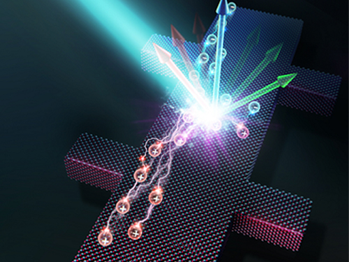
 Highly Efficient and Stable Double Layer Solar Cell Developed
Solar cells convert light into energy, but they can be inefficient and vulnerable to the environment, degrading with, ironically, too much light or other factors, including moisture and low temperature. An international research team has developed a new type of solar cell that can both withstand environmental hazards and is 26.7% efficient in power conversion.
They published their results on March 26 in Science.
The researchers, led by Byungha Shin, a professor from the Department of Materials Science and Engineering at KAIST, focused on developing a new class of light-absorbing material, called a wide bandgap perovskite. The material has a highly effective crystal structure that can process the power needs, but it can become problematic when exposed to environmental hazards, such as moisture. Researchers have made some progress increasing the efficiency of solar cells based on perovskite, but the material has greater potential than what was previously achieved.
To achieve better performance, Shin and his team built a double layer solar cell, called tandem, in which two or more light absorbers are stacked together to better utilize solar energy. To use perovskite in these tandem devices, the scientists modified the material’s optical property, which allows it to absorb a wider range of solar energy. Without the adjustment, the material is not as useful in achieving high performing tandem solar cells. The modification of the optical property of perovskite, however, comes with a penalty — the material becomes hugely vulnerable to the environment, in particular, to light.
To counteract the wide bandgap perovskite’s delicate nature, the researchers engineered combinations of molecules composing a two-dimensional layer in the perovskite, stabilizing the solar cells.
“We developed a high-quality wide bandgap perovskite material and, in combination with silicon solar cells, achieved world-class perovskite-silicon tandem cells,” Shin said.
The development was only possible due to the engineering method, in which the mixing ratio of the molecules building the two-dimensional layer are carefully controlled. In this case, the perovskite material not only improved efficiency of the resulting solar cell but also gained durability, retaining 80% of its initial power conversion capability even after 1,000 hours of continuous illumination. This is the first time such a high efficiency has been achieved with a wide bandgap perovskite single layer alone, according to Shin.
“Such high-efficiency wide bandgap perovskite is an essential technology for achieving ultra-high efficiency of perovskite-silicon tandem (double layer) solar cells,” Shin said. “The results also show the importance of bandgap matching of upper and lower cells in these tandem solar cells.”
The researchers, having stabilized the wide bandgap perovskite material, are now focused on developing even more efficient tandem solar cells that are expected to have more than 30% of power conversion efficiency, something that no one has achieved yet,
“Our ultimate goal is to develop ultra-high-efficiency tandem solar cells that contribute to the increase of shared solar energy among all energy sources,” Shin said. “We want to contribute to making the planet healthier.”
This work was supported by the National Research Foundation of Korea, the Korea Institute of Energy Technology Evaluation and Planning, the Ministry of Trade Industry and Energy of Korea, and the U.S. Department of Energy.
Other contributors include Daehan Kim, Jekyung Kim, Passarut Boonmongkolras, Seong Ryul Pae and Minkyu Kim, all of whom affiliated with the Department of Materials Science and Engineering at KAIST. Other authors include Byron W. Larson, Sean P. Dunfield, Chuanxiao Xiao, Jinhui Tong, Fei Zhang, Joseph J. Berry, Kai Zhu and Dong Hoe Kim, all of who are affiliated with the National Renewable Energy Laboratory in Colorado. Dunfield is also affiliated with the Materials Science and Engineering Program at the University of Colorado; Berry is also affiliated with the Department of Physics and the Renewable and Sustainable Energy Institute at the University of Colorado Boulder; and Kim is also affiliated with the Department of Nanotechnology and Advanced Materials Engineering at Sejong University. Hee Joon Jung and Vinayak Dravid of the Department of Materials Science and Engineering at Northwestern University; Ik Jae Park, Su Geun Ji and Jin Young Kim of the Department of Materials Science and Engineering at Seoul National University; and Seok Beom Kang of the Department of Nanotechnology and Advanced Materials Engineering of Sejong University also contributed.
Image credit: Professor Byungha Shin, KAIST
Image usage restrictions: News organizations may use or redistribute this image, with proper attribution, as part of news coverage of this paper only.
Publication: Kim et al. (2020) “Efficient, stable silicon tandem cells enabled by anion-engineered wide band gap perovskites”. Science. Available online at https://doi.org/10.1126/science.aba3433
Profile:
Byungha Shin
Professor
byungha@kaist.ac.kr
http://energymatlab.kaist.ac.kr/
Department of Materials Science and Engineering
KAIST
Profile:
Daehan Kim
Ph.D. Candidate
zxzx4592@kaist.ac.kr
http://energymatlab.kaist.ac.kr/
Department of Materials Science and Engineering
KAIST
(END)
2020.03.27 View 20996
Highly Efficient and Stable Double Layer Solar Cell Developed
Solar cells convert light into energy, but they can be inefficient and vulnerable to the environment, degrading with, ironically, too much light or other factors, including moisture and low temperature. An international research team has developed a new type of solar cell that can both withstand environmental hazards and is 26.7% efficient in power conversion.
They published their results on March 26 in Science.
The researchers, led by Byungha Shin, a professor from the Department of Materials Science and Engineering at KAIST, focused on developing a new class of light-absorbing material, called a wide bandgap perovskite. The material has a highly effective crystal structure that can process the power needs, but it can become problematic when exposed to environmental hazards, such as moisture. Researchers have made some progress increasing the efficiency of solar cells based on perovskite, but the material has greater potential than what was previously achieved.
To achieve better performance, Shin and his team built a double layer solar cell, called tandem, in which two or more light absorbers are stacked together to better utilize solar energy. To use perovskite in these tandem devices, the scientists modified the material’s optical property, which allows it to absorb a wider range of solar energy. Without the adjustment, the material is not as useful in achieving high performing tandem solar cells. The modification of the optical property of perovskite, however, comes with a penalty — the material becomes hugely vulnerable to the environment, in particular, to light.
To counteract the wide bandgap perovskite’s delicate nature, the researchers engineered combinations of molecules composing a two-dimensional layer in the perovskite, stabilizing the solar cells.
“We developed a high-quality wide bandgap perovskite material and, in combination with silicon solar cells, achieved world-class perovskite-silicon tandem cells,” Shin said.
The development was only possible due to the engineering method, in which the mixing ratio of the molecules building the two-dimensional layer are carefully controlled. In this case, the perovskite material not only improved efficiency of the resulting solar cell but also gained durability, retaining 80% of its initial power conversion capability even after 1,000 hours of continuous illumination. This is the first time such a high efficiency has been achieved with a wide bandgap perovskite single layer alone, according to Shin.
“Such high-efficiency wide bandgap perovskite is an essential technology for achieving ultra-high efficiency of perovskite-silicon tandem (double layer) solar cells,” Shin said. “The results also show the importance of bandgap matching of upper and lower cells in these tandem solar cells.”
The researchers, having stabilized the wide bandgap perovskite material, are now focused on developing even more efficient tandem solar cells that are expected to have more than 30% of power conversion efficiency, something that no one has achieved yet,
“Our ultimate goal is to develop ultra-high-efficiency tandem solar cells that contribute to the increase of shared solar energy among all energy sources,” Shin said. “We want to contribute to making the planet healthier.”
This work was supported by the National Research Foundation of Korea, the Korea Institute of Energy Technology Evaluation and Planning, the Ministry of Trade Industry and Energy of Korea, and the U.S. Department of Energy.
Other contributors include Daehan Kim, Jekyung Kim, Passarut Boonmongkolras, Seong Ryul Pae and Minkyu Kim, all of whom affiliated with the Department of Materials Science and Engineering at KAIST. Other authors include Byron W. Larson, Sean P. Dunfield, Chuanxiao Xiao, Jinhui Tong, Fei Zhang, Joseph J. Berry, Kai Zhu and Dong Hoe Kim, all of who are affiliated with the National Renewable Energy Laboratory in Colorado. Dunfield is also affiliated with the Materials Science and Engineering Program at the University of Colorado; Berry is also affiliated with the Department of Physics and the Renewable and Sustainable Energy Institute at the University of Colorado Boulder; and Kim is also affiliated with the Department of Nanotechnology and Advanced Materials Engineering at Sejong University. Hee Joon Jung and Vinayak Dravid of the Department of Materials Science and Engineering at Northwestern University; Ik Jae Park, Su Geun Ji and Jin Young Kim of the Department of Materials Science and Engineering at Seoul National University; and Seok Beom Kang of the Department of Nanotechnology and Advanced Materials Engineering of Sejong University also contributed.
Image credit: Professor Byungha Shin, KAIST
Image usage restrictions: News organizations may use or redistribute this image, with proper attribution, as part of news coverage of this paper only.
Publication: Kim et al. (2020) “Efficient, stable silicon tandem cells enabled by anion-engineered wide band gap perovskites”. Science. Available online at https://doi.org/10.1126/science.aba3433
Profile:
Byungha Shin
Professor
byungha@kaist.ac.kr
http://energymatlab.kaist.ac.kr/
Department of Materials Science and Engineering
KAIST
Profile:
Daehan Kim
Ph.D. Candidate
zxzx4592@kaist.ac.kr
http://energymatlab.kaist.ac.kr/
Department of Materials Science and Engineering
KAIST
(END)
2020.03.27 View 20996 -
 ‘Carrier-Resolved Photo-Hall’ to Push Semiconductor Advances
(Professor Shin and Dr. Gunawan (left))
An IBM-KAIST research team described a breakthrough in a 140-year-old mystery in physics. The research reported in Nature last month unlocks the physical characteristics of semiconductors in much greater detail and aids in the development of new and improved semiconductor materials.
Research team under Professor Byungha Shin at the Department of Material Sciences and Engineering and Dr. Oki Gunawan at IBM discovered a new formula and technique that enables the simultaneous extraction of both majority and minority carrier information such as their density and mobility, as well as gain additional insights about carrier lifetimes, diffusion lengths, and the recombination process. This new discovery and technology will help push semiconductor advances in both existing and emerging technologies.
Semiconductors are the basic building blocks of today’s digital electronics age, providing us with a multitude of devices that benefit our modern life. To truly appreciate the physics of semiconductors, it is very important to understand the fundamental properties of the charge carriers inside the materials, whether those particles are positive or negative, their speed under an applied electric field, and how densely they are packed into the material.
Physicist Edwin Hall found a way to determine those properties in 1879, when he discovered that a magnetic field will deflect the movement of electronic charges inside a conductor and that the amount of deflection can be measured as a voltage perpendicular to the flow of the charge. Decades after Hall’s discovery, researchers also recognized that they can measure the Hall effect with light via “photo-Hall experiments”. During such experiments, the light generates multiple carriers or electron–hole pairs in the semiconductors.
Unfortunately, the basic Hall effect only provided insights into the dominant charge carrier (or majority carrier). Researchers were unable to extract the properties of both carriers (the majority and minority carriers) simultaneously. The property information of both carriers is crucial for many applications that involve light such as solar cells and other optoelectronic devices.
In the photo-Hall experiment by the KAIST-IBM team, both carriers contribute to changes in conductivity and the Hall coefficient. The key insight comes from measuring the conductivity and Hall coefficient as a function of light intensity. Hidden in the trajectory of the conductivity, the Hall coefficient curve reveals crucial new information: the difference in the mobility of both carriers. As discussed in the paper, this relationship can be expressed elegantly as: Δµ = d (σ²H)/dσ
The research team solved for both majority and minority carrier mobility and density as a function of light intensity, naming the new technique Carrier-Resolved Photo Hall (CRPH) measurement. With known light illumination intensity, the carrier lifetime can be established in a similar way.
Beyond advances in theoretical understanding, advances in experimental techniques were also critical for enabling this breakthrough. The technique requires a clean Hall signal measurement, which can be challenging for materials where the Hall signal is weak due to low mobility or when extra unwanted signals are present, such as under strong light illumination.
The newly developed photo-Hall technique allows the extraction of an astonishing amount of information from semiconductors. In contrast to only three parameters obtained in the classic Hall measurements, this new technique yields up to seven parameters at every tested level of light intensity. These include the mobility of both the electron and hole; their carrier density under light; the recombination lifetime; and the diffusion lengths for electrons, holes, and ambipolar types. All of these can be repeated N times (i.e. the number of light intensity settings used in the experiment).
Professor Shin said, “This novel technology sheds new light on understanding the physical characteristics of semiconductor materials in great detail.” Dr. Gunawan added, “This will will help accelerate the development of next-generation semiconductor technology such as better solar cells, better optoelectronics devices, and new materials and devices for artificial intelligence technology.”
Profile:
Professor Byungha Shin
Department of Materials Science and Engineering
KAIST
byungha@kaist.ac.kr
http://energymatlab.kaist.ac.kr/
2019.11.18 View 14560
‘Carrier-Resolved Photo-Hall’ to Push Semiconductor Advances
(Professor Shin and Dr. Gunawan (left))
An IBM-KAIST research team described a breakthrough in a 140-year-old mystery in physics. The research reported in Nature last month unlocks the physical characteristics of semiconductors in much greater detail and aids in the development of new and improved semiconductor materials.
Research team under Professor Byungha Shin at the Department of Material Sciences and Engineering and Dr. Oki Gunawan at IBM discovered a new formula and technique that enables the simultaneous extraction of both majority and minority carrier information such as their density and mobility, as well as gain additional insights about carrier lifetimes, diffusion lengths, and the recombination process. This new discovery and technology will help push semiconductor advances in both existing and emerging technologies.
Semiconductors are the basic building blocks of today’s digital electronics age, providing us with a multitude of devices that benefit our modern life. To truly appreciate the physics of semiconductors, it is very important to understand the fundamental properties of the charge carriers inside the materials, whether those particles are positive or negative, their speed under an applied electric field, and how densely they are packed into the material.
Physicist Edwin Hall found a way to determine those properties in 1879, when he discovered that a magnetic field will deflect the movement of electronic charges inside a conductor and that the amount of deflection can be measured as a voltage perpendicular to the flow of the charge. Decades after Hall’s discovery, researchers also recognized that they can measure the Hall effect with light via “photo-Hall experiments”. During such experiments, the light generates multiple carriers or electron–hole pairs in the semiconductors.
Unfortunately, the basic Hall effect only provided insights into the dominant charge carrier (or majority carrier). Researchers were unable to extract the properties of both carriers (the majority and minority carriers) simultaneously. The property information of both carriers is crucial for many applications that involve light such as solar cells and other optoelectronic devices.
In the photo-Hall experiment by the KAIST-IBM team, both carriers contribute to changes in conductivity and the Hall coefficient. The key insight comes from measuring the conductivity and Hall coefficient as a function of light intensity. Hidden in the trajectory of the conductivity, the Hall coefficient curve reveals crucial new information: the difference in the mobility of both carriers. As discussed in the paper, this relationship can be expressed elegantly as: Δµ = d (σ²H)/dσ
The research team solved for both majority and minority carrier mobility and density as a function of light intensity, naming the new technique Carrier-Resolved Photo Hall (CRPH) measurement. With known light illumination intensity, the carrier lifetime can be established in a similar way.
Beyond advances in theoretical understanding, advances in experimental techniques were also critical for enabling this breakthrough. The technique requires a clean Hall signal measurement, which can be challenging for materials where the Hall signal is weak due to low mobility or when extra unwanted signals are present, such as under strong light illumination.
The newly developed photo-Hall technique allows the extraction of an astonishing amount of information from semiconductors. In contrast to only three parameters obtained in the classic Hall measurements, this new technique yields up to seven parameters at every tested level of light intensity. These include the mobility of both the electron and hole; their carrier density under light; the recombination lifetime; and the diffusion lengths for electrons, holes, and ambipolar types. All of these can be repeated N times (i.e. the number of light intensity settings used in the experiment).
Professor Shin said, “This novel technology sheds new light on understanding the physical characteristics of semiconductor materials in great detail.” Dr. Gunawan added, “This will will help accelerate the development of next-generation semiconductor technology such as better solar cells, better optoelectronics devices, and new materials and devices for artificial intelligence technology.”
Profile:
Professor Byungha Shin
Department of Materials Science and Engineering
KAIST
byungha@kaist.ac.kr
http://energymatlab.kaist.ac.kr/
2019.11.18 View 14560