Byung+Jin+Cho
-
 Research Day Highlights Most Outstanding Research Achievements
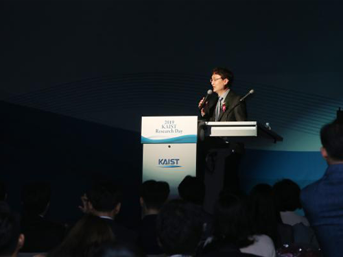
Professor Byung Jin Cho from the School of Electrical Engineering was selected as the Grand Research Prize Winner in recognition of his innovative research achievement in the fields of nano electric and flexible energy devices during the 2019 KAIST Research Day ceremony held on April 23 at the Chung Kunmo Conference Hall.
The ten most outstanding research achievements from the past year were also awarded in the three areas of Research, Innovation, Convergence Researches.
Professor Cho is an internationally recognized researcher in the field of future nano and energy device technology. Professor Cho’s team has continued to research on advanced CMOS (complementary metal-oxide semiconductors). CMOS has become his key research topic over the past three decades.
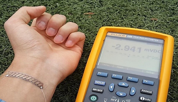
In 2014, he developed a glass fabric-based thermoelectric generator, which is extremely light and flexible and produces electricity from the heat of the human body. It is so flexible that the allowable bending radius of the generator is as low as 20 mm. There are no changes in performance even if the generator bends upward and downward for up to 120 cycles. His wearable thermoelectric generator was selected as one of the top ten most promising digital technologies by the Netexplo Forum in 2015.
He now is working on high-performance and ultra-flexible CMOS IC for biomedical applications, expanding his scope to thermal haptic technology in VR using graphene-CMOS hybrid integrated circuits; to self-powered wireless sensor nodes and self-powered ECG system using wearable thermoelectric generators .
In his special lecture at the ceremony, Professor Cho stressed the importance of collaboration in making scientific research and presented how he moved to future devices after focusing on scaling the devices.
“When I started the research on semiconductors, I focused on how to scale the device down as much as possible. For decades, we have conducted a number of procedures to produce tiny but efficient materials. Now we have shifted to develop flexible thermoelements and wearable devices,” said Professor Cho.
“We all thought the scaling down is the only way to create value-added technological breakthroughs. Now, the devices have been scaled down to 7nm and will go down to 5 nm soon. Over the past few years, I think we have gone through all the possible technological breakthroughs for reducing the size to 5nm. The semiconductor devices are made of more 1 billion transistors and go through 1,000 technological processes. So, there won’t be any possible way for a single genius to make a huge breakthrough. Without collaboration with others, it is nearly impossible to make any new technological breakthroughs.”
Professor Cho has published more than 240 papers in renowned academic journals and presented more than 300 papers at academic conferences. He has also registered approximately 50 patents in the field of semiconductor device technology.
The top ten research highlights of 2018 as follows:
- Rydberg-Atom Quantum Simulator Development by Professor Jaewook Ahn and Heung-Sun Sim from the Department of Physics
- From C-H to C-C Bonds at Room Temperature by Professor Mu-Hyun Baik from the Department of Chemistry
- The Role of Rodlike Counterions on the Interactions of DNAs by Professor Yong Woon Kim of the Graduate School of Nanoscience and Technology
- The Medal Preoptic Area Induces Hunting-Like Behaviors to Target Objects and Prey by Professor Daesoo Kim from the Department of Biological Sciences
- Identification of the Origin of Brain Tumors and New Therapeutic Strategy by Professor Jeong Ho Lee from the Graduate School of Medical Science and Engineering
- The Linear Frequency Conversion of Light at a Spatiotemporal Boundary by Professor Bumki Min from the Department of Mechanical Engineering
- An Industrial Grade Flexible Transparent Force Touch Sensor by Professor Jun-Bo Yoon from the School of Electrical Engineering
- The Detection and Clustering of Mixed-Type Defect Patterns in Wafer Bin Maps by Professor Heeyoung Kim from the Department of Industrial and Systems Engineering
- The Development of a Reconfigurable Spin-Based Logic Device by Professor Byong-Guk Park from the Department of Materials Science and Engineering
- The Development of a Miniaturized X-Ray Tube Based on Carbon Nanotube and Electronic Brachytherapy Device by Professor Sung Oh Cho from the Department of Nuclear and Quantum Engineering
Professor YongKeun Park from the Department of Physics and Professor In-Chel Park from the School of Electrical Engineering received the Research Award. For the Innovation Award, Professor Munchurl Kim from the School of Electrical Engineering was the recipient and the Convergence Research Awards was conferred to Professor Sung-Yool Choi from the School of Electrical Engineering, Professor Sung Gap Im from the Department of Chemical and Biomolecular Engineering, and Professor SangHee Park from the Department of Materials Science and Engineering during the ceremony.
For more on KAIST’s Top Research Achievements and Highlight of 2018, please refer to the attached below. click.
2019.04.25 View 18522
Research Day Highlights Most Outstanding Research Achievements
Professor Byung Jin Cho from the School of Electrical Engineering was selected as the Grand Research Prize Winner in recognition of his innovative research achievement in the fields of nano electric and flexible energy devices during the 2019 KAIST Research Day ceremony held on April 23 at the Chung Kunmo Conference Hall.
The ten most outstanding research achievements from the past year were also awarded in the three areas of Research, Innovation, Convergence Researches.
Professor Cho is an internationally recognized researcher in the field of future nano and energy device technology. Professor Cho’s team has continued to research on advanced CMOS (complementary metal-oxide semiconductors). CMOS has become his key research topic over the past three decades.
In 2014, he developed a glass fabric-based thermoelectric generator, which is extremely light and flexible and produces electricity from the heat of the human body. It is so flexible that the allowable bending radius of the generator is as low as 20 mm. There are no changes in performance even if the generator bends upward and downward for up to 120 cycles. His wearable thermoelectric generator was selected as one of the top ten most promising digital technologies by the Netexplo Forum in 2015.
He now is working on high-performance and ultra-flexible CMOS IC for biomedical applications, expanding his scope to thermal haptic technology in VR using graphene-CMOS hybrid integrated circuits; to self-powered wireless sensor nodes and self-powered ECG system using wearable thermoelectric generators .
In his special lecture at the ceremony, Professor Cho stressed the importance of collaboration in making scientific research and presented how he moved to future devices after focusing on scaling the devices.
“When I started the research on semiconductors, I focused on how to scale the device down as much as possible. For decades, we have conducted a number of procedures to produce tiny but efficient materials. Now we have shifted to develop flexible thermoelements and wearable devices,” said Professor Cho.
“We all thought the scaling down is the only way to create value-added technological breakthroughs. Now, the devices have been scaled down to 7nm and will go down to 5 nm soon. Over the past few years, I think we have gone through all the possible technological breakthroughs for reducing the size to 5nm. The semiconductor devices are made of more 1 billion transistors and go through 1,000 technological processes. So, there won’t be any possible way for a single genius to make a huge breakthrough. Without collaboration with others, it is nearly impossible to make any new technological breakthroughs.”
Professor Cho has published more than 240 papers in renowned academic journals and presented more than 300 papers at academic conferences. He has also registered approximately 50 patents in the field of semiconductor device technology.
The top ten research highlights of 2018 as follows:
- Rydberg-Atom Quantum Simulator Development by Professor Jaewook Ahn and Heung-Sun Sim from the Department of Physics
- From C-H to C-C Bonds at Room Temperature by Professor Mu-Hyun Baik from the Department of Chemistry
- The Role of Rodlike Counterions on the Interactions of DNAs by Professor Yong Woon Kim of the Graduate School of Nanoscience and Technology
- The Medal Preoptic Area Induces Hunting-Like Behaviors to Target Objects and Prey by Professor Daesoo Kim from the Department of Biological Sciences
- Identification of the Origin of Brain Tumors and New Therapeutic Strategy by Professor Jeong Ho Lee from the Graduate School of Medical Science and Engineering
- The Linear Frequency Conversion of Light at a Spatiotemporal Boundary by Professor Bumki Min from the Department of Mechanical Engineering
- An Industrial Grade Flexible Transparent Force Touch Sensor by Professor Jun-Bo Yoon from the School of Electrical Engineering
- The Detection and Clustering of Mixed-Type Defect Patterns in Wafer Bin Maps by Professor Heeyoung Kim from the Department of Industrial and Systems Engineering
- The Development of a Reconfigurable Spin-Based Logic Device by Professor Byong-Guk Park from the Department of Materials Science and Engineering
- The Development of a Miniaturized X-Ray Tube Based on Carbon Nanotube and Electronic Brachytherapy Device by Professor Sung Oh Cho from the Department of Nuclear and Quantum Engineering
Professor YongKeun Park from the Department of Physics and Professor In-Chel Park from the School of Electrical Engineering received the Research Award. For the Innovation Award, Professor Munchurl Kim from the School of Electrical Engineering was the recipient and the Convergence Research Awards was conferred to Professor Sung-Yool Choi from the School of Electrical Engineering, Professor Sung Gap Im from the Department of Chemical and Biomolecular Engineering, and Professor SangHee Park from the Department of Materials Science and Engineering during the ceremony.
For more on KAIST’s Top Research Achievements and Highlight of 2018, please refer to the attached below. click.
2019.04.25 View 18522 -
 KAIST's Thermoelectric Generator on Glass Fabric Receives the Grand Prize at the Netexplo Forum 2015
The forum announced top ten IT innovations expected to change the world and selected the grand prize on February 4, 2014.
Established in 2007 by Martine Bidegain and Thierry Happe in partnership with the French Senate and the French Ministry for the Digital Economy, the Netexplo Observatory is an independent global organization that studies the impact of digital technology and innovation on society and business.
Every year, the Netexplo Observatory hosts an international conference, the Netexplo Forum, in Paris, France, which surveys digital innovation worldwide. The 8th forum was held in partnership with the United Nations Educational, Scientific and Cultural Organization (UNESCO) on February 4-5, 2015, at the UNESCO House in Paris.
Prior to the conference, the Netexplo Forum 2015 named the top ten most promising digital technologies that will greatly impact the world.
Among them was Professor Byung Jin Cho’s research on a wearable thermoelectric generator (http://www.eurekalert.org/pub_releases/2014-04/tkai-tgo041014.php). The generator was selected as the most innovative technology this year.
Professor Cho of KAIST’s Electrical Engineering Department developed a glass fabric-based thermoelectric generator that is extremely light and flexible and that produces electricity from the heat of the human body. This technology can be applied widely to wearable computers and mobile devices.
The full list of innovations follows below:
Wearable Thermo-Element, South Korea: The human body becomes a source of energy for mobile devices.
W.Afate 3D-printer, Togo: An environmentally friendly fablab that makes a low-cost 3D-printer from recycling electronic components.
Slack, USA: By combining email, Skype, and file-sharing and social networks, internal communication becomes much easier and simpler.
PhotoMath, Croatia: A free app that enables smartphone users to solve mathematical problems simply by scanning the mathematical texts.
Kappo, Chile: Connected cyclists produce and transmit useful data for urban planning to make the city more bike-friendly.
Branching Minds, USA: An improved learning process for students in difficulty through a personalized approach.
Baidu Kuai Sou, China: Smart chopsticks that can check food hazards.
SCio, Israel: A pocket molecular sensor with various applications and data
Rainforest Connection, USA: Fighting deforestation with recycled smartphones
Sense Ebola Followup, Nigeria: A mobile tool to help contain Ebola
For more details on the wearable thermos-element which received the 2015 Netexplo Award, please go to https://www.netexplo.org/en/intelligence/innovation/wearable-thermo-element.
Pictures 1 and 2: A high-performance wearable thermoelectric generator that is extremely flexible and light.
Picture 3: Senator Catherine Morin-Desailly (left) of the French Parliament presents the 2015 Netexplo Award to Professor Byung Jin Cho (right) on February 4, 2015 at the UNESCO House in Paris.
Credit of Loran Dhérines
Picture 4: Professor Byung Jin Cho (left) poses with Dr. Joël de Rosnay (right).
Credit of Loran Dhérines
2015.02.06 View 16312
KAIST's Thermoelectric Generator on Glass Fabric Receives the Grand Prize at the Netexplo Forum 2015
The forum announced top ten IT innovations expected to change the world and selected the grand prize on February 4, 2014.
Established in 2007 by Martine Bidegain and Thierry Happe in partnership with the French Senate and the French Ministry for the Digital Economy, the Netexplo Observatory is an independent global organization that studies the impact of digital technology and innovation on society and business.
Every year, the Netexplo Observatory hosts an international conference, the Netexplo Forum, in Paris, France, which surveys digital innovation worldwide. The 8th forum was held in partnership with the United Nations Educational, Scientific and Cultural Organization (UNESCO) on February 4-5, 2015, at the UNESCO House in Paris.
Prior to the conference, the Netexplo Forum 2015 named the top ten most promising digital technologies that will greatly impact the world.
Among them was Professor Byung Jin Cho’s research on a wearable thermoelectric generator (http://www.eurekalert.org/pub_releases/2014-04/tkai-tgo041014.php). The generator was selected as the most innovative technology this year.
Professor Cho of KAIST’s Electrical Engineering Department developed a glass fabric-based thermoelectric generator that is extremely light and flexible and that produces electricity from the heat of the human body. This technology can be applied widely to wearable computers and mobile devices.
The full list of innovations follows below:
Wearable Thermo-Element, South Korea: The human body becomes a source of energy for mobile devices.
W.Afate 3D-printer, Togo: An environmentally friendly fablab that makes a low-cost 3D-printer from recycling electronic components.
Slack, USA: By combining email, Skype, and file-sharing and social networks, internal communication becomes much easier and simpler.
PhotoMath, Croatia: A free app that enables smartphone users to solve mathematical problems simply by scanning the mathematical texts.
Kappo, Chile: Connected cyclists produce and transmit useful data for urban planning to make the city more bike-friendly.
Branching Minds, USA: An improved learning process for students in difficulty through a personalized approach.
Baidu Kuai Sou, China: Smart chopsticks that can check food hazards.
SCio, Israel: A pocket molecular sensor with various applications and data
Rainforest Connection, USA: Fighting deforestation with recycled smartphones
Sense Ebola Followup, Nigeria: A mobile tool to help contain Ebola
For more details on the wearable thermos-element which received the 2015 Netexplo Award, please go to https://www.netexplo.org/en/intelligence/innovation/wearable-thermo-element.
Pictures 1 and 2: A high-performance wearable thermoelectric generator that is extremely flexible and light.
Picture 3: Senator Catherine Morin-Desailly (left) of the French Parliament presents the 2015 Netexplo Award to Professor Byung Jin Cho (right) on February 4, 2015 at the UNESCO House in Paris.
Credit of Loran Dhérines
Picture 4: Professor Byung Jin Cho (left) poses with Dr. Joël de Rosnay (right).
Credit of Loran Dhérines
2015.02.06 View 16312