Advanced+Display
-
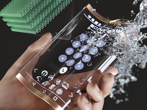 A KAIST research team develops a washable, transparent, and flexible OLED with MXene nanotechnology
Transparent and flexible displays, which have received a lot of attention in various fields including automobile displays, bio-healthcare, military, and fashion, are in fact known to break easily when experiencing small deformations. To solve this problem, active research is being conducted on many transparent and flexible conductive materials such as carbon nanotubes, graphene, silver nanowires, and conductive polymers.
On June 13, a joint research team led by Professor Kyung Cheol Choi from the KAIST School of Electrical Engineering and Dr. Yonghee Lee from the National Nano Fab Center (NNFC) announced the successful development of a water-resistant, transparent, and flexible OLED using MXene nanotechnology. The material can emit and transmit light even when exposed to water.
MXene is a 2D material with high electrical conductivity and optical transmittance, and it can be produced on a large scale through solution processes. However, despite these attractive properties, MXene’s applications were limited as a long-term electrical device due to its electrical properties being degraded easily by atmospheric moisture and water. The material was therefore unable to be systemized into the form of a matrix that can display information.
Professor Choi’s research team used an encapsulation tactic that can protect materials from oxidation caused by moisture and oxygen to develop a MXene-based OLED with a long lifespan and high stability against external environmental factors. The research team first focused on analyzing the degradation mechanism of MXene’s electrical conductivity, and then concentrated on designing an encapsulation membrane. The team blocked moisture and provided flexibility through residual stress offset, ultimately producing a double-layered encapsulation membrane. In addition, a thin plastic film with a thickness of a few micrometers was attached to the top layer to allow washing in water without degradation.
< Figure 1. (a) Transparent passive-matrix display made of MXene-based OLED, (b) Cross-sectional image of MXene-based OLED observed by transmission electron microscope (TEM), (c) Electro-optical characteristic graph of red, green, and blue MXene-based OLED >
Through this study, the research team developed a MXene-based red(R)/green(G)/blue(B) OLED that emits a brightness of over 1,000 cd/m2 that is detectable by the naked eye even under sunlight, thereby meeting the conditions for outdoor displays. As for the red MXene-based OLED, the researchers confirmed a standby storage life of 2,000 hours (under 70% luminescence), a standby operation life of 1,500 hours (under 60% luminescence), and a flexibility withstanding 1,000 cycles under a low curvature of under 1.5mm. In addition, they showed that its performance was maintained even after six hours of immersion under water (under 80% luminescence). Furthermore, a patterning technique was used to produce the MXene-based OLED in the form of a passive matrix, and the team demonstrated its use as a transparent display by displaying letters and shapes.
Ph.D. candidate So Yeong Jeong, who led this study, said, “To improve the reliability of MXene OLED, we focused on producing an adequate encapsulation structure and a suitable process design.” She added, “By producing a matrix-type MXene OLED and displaying simple letters and shapes, we have laid the foundations for MXene’s application in the field of transparent displays.”
< Image 1. Cover of ACS Nano Front Cover (Conceptual diagram of MXene-based OLED display) >
Professor Choi said, “This research will become the guideline for applying MXene in electrical devices, but we expect for it to also be applied in other fields that require flexible and transparent displays like automobiles, fashion, and functional clothing. And to widen the gap with China’s OLED technology, these new OLED convergence technologies must continue to be developed.”
This research was supported by the National Research Foundation of Korea and funded by the Ministry of Science and ICT, Korea. It was published as a front cover story of ACS Nano under the title, “Highly Air-Stable, Flexible, and Water-Resistive 2D Titanium Carbide MXene-Based RGB Organic Light-Emitting Diode Displays for Transparent Free-Form Electronics” on June 13.
2023.07.10 View 7972
 -
 Stress-Relief Substrate Helps OLED Stretch Two-Dimensionally
Highly functional and free-form displays are critical components to complete the technological prowess of wearable electronics, robotics, and human-machine interfaces.
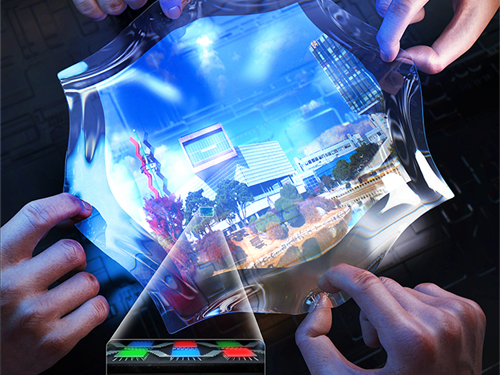
A KAIST team created stretchable OLEDs (Organic Light-Emitting Diodes) that are compliant and maintain their performance under high-strain deformation. Their stress-relief substrates have a unique structure and utilize pillar arrays to reduce the stress on the active areas of devices when strain is applied.
Traditional intrinsically stretchable OLEDs have commercial limitations due to their low efficiency in the electrical conductivity of the electrodes. In addition, previous geometrically stretchable OLEDs laminated to the elastic substrates with thin film devices lead to different pixel emissions of the devices from different peak sizes of the buckles.
To solve these problems, a research team led by Professor Kyung Cheol Choi designed a stretchable substrate system with surface relief island structures that relieve the stress at the locations of bridges in the devices. Their stretchable OLED devices contained an elastic substrate structure comprising bonded elastic pillars and bridges. A patterned upper substrate with bridges makes the rigid substrate stretchable, while the pillars decentralize the stress on the device.
Although various applications using micropillar arrays have been reported, it has not yet been reported how elastic pillar arrays can affect substrates by relieving the stress applied to those substrates upon stretching. Compared to results using similar layouts with conventional free-standing, flat substrates or island structures, their results with elastic pillar arrays show relatively low stress levels at both the bridges and plates when stretching the devices. They achieved stretchable RGB (red, green, blue) OLEDs and had no difficulties with material selection as practical processes were conducted with stress-relief substrates.
Their stretchable OLEDs were mechanically stable and have two-dimensional stretchability, which is superior to only one-direction stretchable electronics, opening the way for practical applications like wearable electronics and health monitoring systems.
Professor Choi said, “Our substrate design will impart flexibility into electronics technology development including semiconductor and circuit technologies. We look forward this new stretchable OLED lowering the barrier for entering the stretchable display market.”
This research was published in Nano Letters titled Two-Dimensionally Stretchable Organic Light-Emitting Diode with Elastic Pillar Arrays for Stress Relief. (https://dx.doi.org/10.1021/acs.nanolett.9b03657). This work was supported by the Engineering Research Center of Excellence Program supported by the National Research Foundation of Korea.
-Profile
Professor Kyung Cheol Choi
kyungcc@kaist.ac.kr
http://adnc.kaist.ac.kr/
School of Electrical Engineering
KAIST
2020.02.27 View 10541
 -
 New Technology Will Enable the Commercialization of Plasmon Displays
-- Enhancements in the penetration ratios of color filters are expected by applying nano-surface plasmon effects. --
-- Color filter technology will be applicable to large-area OLED and LCD. --
The fabrication technology to commercialize display color filters using plasmon effects has been discovered.
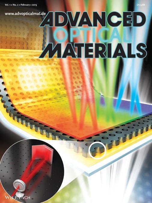
A joint research team headed by Professor Kyung Cheol Choi from the Department of Electrical Engineering of the Korea Advanced Institute for Science and Technology and Prof. Byeong-Kwon Ju from the School of Electrical Engineering of Korea University has developed the technology to design and produce a display color filter by applying nano-surface plasmon effects.
Color filters are core components used to express colors in CMOS image sensors found in LCD/OLED displays or digital cameras. The current color filters have penetration ratios of 20~30%, but the objective of the joint research team is to raise this penetration ratio by over 40% to facilitate the mass production of energy-efficient plasmonic displays.
Currently available plasmonic color filters are limited to applications on micrometer scales. However, outcomes of the newest research extend the size of the applications up to 2.5 cm by using laser interference lithography. The academic and industrial sectors agree that it is now possible to mass-produce displays using plasmonic color filters.
The researchers built a nanohole array to large scale by using laser interference lithography, a technology that forms nanostructures with laser light interferences. They also suggested a new manufacturing process that can optimize the features of color filters while compensating for defects arising from the fabrication stages.
The new manufacturing process of applying laser interference lithography is expected to overcome the shortcomings of traditional color filters by simplifying production and, enabling them to be produced at lower costs.
“There were limitations to industrial applications of plasmon effect due to production costs, time, and yields,” explained Yun Seon Do, a Ph. D. candidate in the Department of Electrical Engineering of KAIST. “The new technology can reduce fabrication time and cost to the extent that it would be advisable to replace dye-based and pigment-based color filter technology."
“This research can be applied to large-scale displays, such as TV screens, by using laser-interference lithography,” said Jung-Ho Park, a Ph. D. candidate in the School of Electrical Engineering of Korea University. “The research outcome is expected to be widely applied in advanced nano-manufacturing processes as it does not restrict the types of circuit boards."
The research outcome, led by doctoral candidates Do and Park, appeared on the front cover of the second issue of Advanced Optical Materials, a highly regarded academic journal in the field of nanotechnologies, and the team has applied for six related patents.
2013.03.13 View 10157
 -
 Prof. Choi Unveils Method to Improve Emission Efficiency of OLED
A KAIST research team led by Prof. Kyung-Cheol Choi of the School of Electrical Engineering & Computer Science discovered the surface plasmon-enhanced spontaneous emission based on an organic light-emitting device (OLED), a finding expected to improve OLED"s emission efficiency, KAIST authorities said on Thursday (July 9).
For surface plasmon localization, silver nanoparticles were thermally deposited in a high vacuum on cathode. Since plasmons provide a strong oscillator decay channel, time-resolved photoluninescene (PL) results displayed a 1.75-fold increased emission rate, and continuous wave PL results showed a twofold enhanced intensity.
"The method using surface plasmon represents a new technology to enhance the emission efficiency of OLED. It is expected to greatly contribute to the development of new technologies in OLED and flexible display, as well as securing original technology," Prof. Choi said.
The finding was published in the April issue of Applied Physics Letters and the June 25 issue of Optics Express. It will be also featured as the research highlight of the August issue of Nature Photonics and Virtual Journal of Ultrafast Science.
2009.07.09 View 23095
 -
 KAIST to hold International Workshop on Flexible Displays
The 2009 KAIST International Workshop on Flexible Displays will take place at the Electrical Engineering Building on June 25, university sources said on Tuesday (June 23).
The workshop organized by the Center for Advanced Flexible Display Convergence (CAFDC) will explore the status and future vision of flexible and transparent plasma displays, which are among the key technologies for the development of the next-generation displays. There will be also discussions about technologies to realize the large-scale flexible and transparent display which is regarded as the display of the future.
Among the speakers are some of the most prominent figures in the field. Gary Eden from University of Illinois, Prof. Kunihide Tachibana from Kyoto University, and Carol Wedding, the president of Imaging Systems Tech., USA and several other well-known professors and engineers will participate in the workshop.
Professor Kyung-Cheol Choi, CAFDC chair, said: "The workshop will provide an excellent opportunity to examine the flexible and transparent plasma display technologies. It will also be a good chance to explore large-scale flexible and transparent displays from various technical viewpoints."
2009.06.24 View 21429
 -
 International Workshop on Flexible Displays Held on Aug. 21-22
An international workshop on flexible displays will be held at KAIST on Aug. 21-22.
The workshop organized by Center for Advanced Flexible Display Convergence (CAFDC) in KAIST is designed to share ideas on the latest research developments and explore future trends in organic displays. Organic displays made from organic light-emitting diode (OLED) materials have recently made a real impact in consumer electronics and emerged as one of the most important technologies in the development of next-generation flexible displays.
"The workshop is expected to provide an important opportunity to showcase latest technological developments using organic light-emitting diode and examine them from the perspectives of the next-generation flexible display," said Dr. Kyung-Cheol Choi, KAIST professor of electrical engineering and computer science who heads the CAFDC.
The event will feature some of the world-renowned scholars in organic display including Prof. Stephen R. Forrest of the University of Michigan, Prof. Bernard Kippelen of Georgia Tech, and Prof. Takao Someya of the University of Tokyo, as theme presenters. It will also draw a slew of domestic scholars in the industry and academia.
2008.08.22 View 17832
 -
 Prototype technologies for world highest efficiency PDP lightening developed by Prof. Choi
- Core technologies that will solve power consumption problems in PDPs- To be unveiled as invited paper at conference by Society for Information Display in May
A domestic research team has developed prototype technologies for high efficiency lightening that can significantly improve the power consumption of Plasma Display Panels (PDP).
A team headed by Kyung Cheol Choi, a professor of Electrical & Computer Science in KAiST (President Nam-Pyo Suh), has developed new cell structures and driving methods of PDP, typical digital television, which can increase the luminous efficacy of PDP four times and are to be unveiled at the conference by the Society for Information Display (SID) as an invited paper. The SID is the world largest information display society and the conference will be held at Long Beach, CA, U.S. on May 21.
Prof. Choi
2007.04.18 View 14889
 -
 Yoonsun Doh Wins 'Outstanding Poster Paper Award' at IDW
Yoonsun Doh Wins ‘Outstanding Poster Paper Award’ at IDW
Yoonsun Doh, a master-course student at the Division of Electrical Engineering (Advisory professor Kyungchul Choi) won the Outstanding Poster Paper Award at IDW 2006, which was held at Otsu, Japan on December 8, 2006.
The title of Doh’s paper is ‘Relationship between IR Emission of Reset Discharge and Image Retention in AC PDP’.
At the paper, Doh proposed a method capable of quantitatively measuring the temporary image-sticking phenomena, which is raised as a problem that impairs the quality of images on an AC PDP.
2006.12.26 View 16338