%73%65%6e%73%6f%72
-
 KAIST Overcomes Limitations of Existing Image Sensors… Clear Colors Even Under Oblique Light
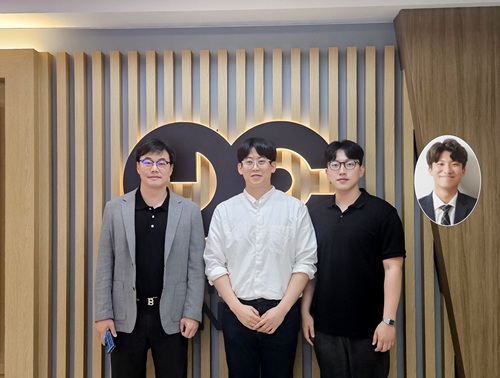
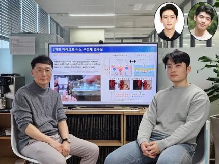
<(From Left) Ph.D candidate Chanhyung Park from Electrical Engineering, Jaehyun Jeon from Department of Physics, Professor Min Seok Jang from Electrical Engineering>
Smartphone cameras are becoming smaller, yet photos are becoming sharper. Korean researchers have elevated the limits of next-generation smartphone cameras by developing a new image sensor technology that can accurately represent colors regardless of the angle at which light enters. The team achieved this by utilizing a “metamaterial” that designs the movement of light through structures too small to be seen with the naked eye.
KAIST (President Kwang Hyung Lee) announced on the 12th of February that a research team led by Professor Min Seok Jang of the School of Electrical Engineering, in collaboration with Professor Haejun Chung’s team at Hanyang, has developed a metamaterial-based technology for image sensors that can stably separate colors even when the angle of light incidence varies.
Conventional smartphone cameras capture images by concentrating light into a small lens. However, as camera pixels become extremely small, lenses alone struggle to gather sufficient light. To address this, the Nanophotonic Color Router was introduced. Instead of concentrating light through a lens, this technology uses microscopic structures invisible to the eye to precisely separate incoming light by color. By designing the pathways through which light travels, this metamaterial-based structure accurately divides light into red (R), green (G), and blue (B).
Samsung Electronics has already demonstrated the commercialization potential of this technology by applying it to actual image sensors under the name “Nano Prism.” Theoretically, stacking multiple layers of extremely fine nanostructures enables greater light collection and more accurate color separation.
<Nanophotonic color router technology that works reliably even under oblique incidence conditions (AI-generated image)>
However, existing Nanophotonic Color Routers had limitations. While they functioned well when light entered vertically, their performance deteriorated significantly—or colors mixed—when light entered at an angle, as is common in smartphone cameras. This issue, known as the “oblique incidence problem,” has been considered a critical challenge that must be resolved for real-world product applications.
The research team first investigated the root cause of this issue. They found that previous designs were overly optimized for vertically incident light, causing performance to drop sharply even with slight changes in the angle of incidence. Since smartphone cameras receive light from various angles, maintaining performance under angular variation is essential.
Instead of manually designing the structure, the team adopted an “inverse design” approach, which allows the computer to autonomously determine the optimal structure. Through this method, they derived a color router design capable of stable color separation even when the angle of incoming light changes.
As a result, whereas previous structures nearly failed when light was tilted by about 12 degrees, the newly designed structure maintained approximately 78% optical efficiency within a ±12-degree range, demonstrating stable color separation performance. In other words, the technology reaches a level suitable for practical smartphone usage environments.
<Nanophotonic color router robust to oblique incidence>
The team further analyzed performance variations by considering factors such as the number of metamaterial layers, design conditions, and potential fabrication errors. They also systematically defined the limits of robustness against changes in the angle of incidence. This study is particularly meaningful in that it presents design criteria for color routers that reflect realistic image sensor environments.
Professor Min Seok Jang of KAIST stated, “This research is significant in that it systematically analyzes the oblique incidence problem, which has hindered the commercialization of color router technology, and proposes a clear solution direction,” adding, “The proposed design methodology can be extended beyond color routers to a wide range of metamaterial-based nanophotonic devices.”
In this study, KAIST undergraduate student Jaehyun Jeon and doctoral candidate Chanhyung Park participated as co-first authors. The research findings were published on January 27 in the international journal Advanced Optical Materials.
※ Paper title: “Inverse Design of Nanophotonic Color Router Robust to Oblique Incidence”
DOI: https://doi.org/10.1002/adom.202501697※ Authors: Jaehyun Jeon (KAIST, first author), Chanhyung Park (KAIST, first author), Doyoung Heo (KAIST), Haejun Chung (Hanyang University), Min Seok Jang (KAIST, corresponding author)
This research was supported by the Ministry of Trade, Industry & Energy (Korea Institute for Advancement of Technology, Korea Semiconductor Research Consortium) under the project “Design Technology of Meta-Optical Structures for Next-Generation Sensors,” by the Ministry of Science and ICT (National Research Foundation of Korea) under the projects “Development of Full-Color Micro LED Devices and Panels Based on Beam-Steerable High-Color-Purity Meta Color Conversion Layers” and “Development of a Real-Time Zero-Energy Argos-Eye Metasurface Network Computing with All Properties of Light,” and by the Ministry of Culture, Sports and Tourism (Korea Creative Content Agency) under the project “International Joint Research for Next-Generation Copyright Protection and Secure Content Distribution Technologies.”
2026.02.19 View 1457
KAIST Overcomes Limitations of Existing Image Sensors… Clear Colors Even Under Oblique Light
<(From Left) Ph.D candidate Chanhyung Park from Electrical Engineering, Jaehyun Jeon from Department of Physics, Professor Min Seok Jang from Electrical Engineering>
Smartphone cameras are becoming smaller, yet photos are becoming sharper. Korean researchers have elevated the limits of next-generation smartphone cameras by developing a new image sensor technology that can accurately represent colors regardless of the angle at which light enters. The team achieved this by utilizing a “metamaterial” that designs the movement of light through structures too small to be seen with the naked eye.
KAIST (President Kwang Hyung Lee) announced on the 12th of February that a research team led by Professor Min Seok Jang of the School of Electrical Engineering, in collaboration with Professor Haejun Chung’s team at Hanyang, has developed a metamaterial-based technology for image sensors that can stably separate colors even when the angle of light incidence varies.
Conventional smartphone cameras capture images by concentrating light into a small lens. However, as camera pixels become extremely small, lenses alone struggle to gather sufficient light. To address this, the Nanophotonic Color Router was introduced. Instead of concentrating light through a lens, this technology uses microscopic structures invisible to the eye to precisely separate incoming light by color. By designing the pathways through which light travels, this metamaterial-based structure accurately divides light into red (R), green (G), and blue (B).
Samsung Electronics has already demonstrated the commercialization potential of this technology by applying it to actual image sensors under the name “Nano Prism.” Theoretically, stacking multiple layers of extremely fine nanostructures enables greater light collection and more accurate color separation.
<Nanophotonic color router technology that works reliably even under oblique incidence conditions (AI-generated image)>
However, existing Nanophotonic Color Routers had limitations. While they functioned well when light entered vertically, their performance deteriorated significantly—or colors mixed—when light entered at an angle, as is common in smartphone cameras. This issue, known as the “oblique incidence problem,” has been considered a critical challenge that must be resolved for real-world product applications.
The research team first investigated the root cause of this issue. They found that previous designs were overly optimized for vertically incident light, causing performance to drop sharply even with slight changes in the angle of incidence. Since smartphone cameras receive light from various angles, maintaining performance under angular variation is essential.
Instead of manually designing the structure, the team adopted an “inverse design” approach, which allows the computer to autonomously determine the optimal structure. Through this method, they derived a color router design capable of stable color separation even when the angle of incoming light changes.
As a result, whereas previous structures nearly failed when light was tilted by about 12 degrees, the newly designed structure maintained approximately 78% optical efficiency within a ±12-degree range, demonstrating stable color separation performance. In other words, the technology reaches a level suitable for practical smartphone usage environments.
<Nanophotonic color router robust to oblique incidence>
The team further analyzed performance variations by considering factors such as the number of metamaterial layers, design conditions, and potential fabrication errors. They also systematically defined the limits of robustness against changes in the angle of incidence. This study is particularly meaningful in that it presents design criteria for color routers that reflect realistic image sensor environments.
Professor Min Seok Jang of KAIST stated, “This research is significant in that it systematically analyzes the oblique incidence problem, which has hindered the commercialization of color router technology, and proposes a clear solution direction,” adding, “The proposed design methodology can be extended beyond color routers to a wide range of metamaterial-based nanophotonic devices.”
In this study, KAIST undergraduate student Jaehyun Jeon and doctoral candidate Chanhyung Park participated as co-first authors. The research findings were published on January 27 in the international journal Advanced Optical Materials.
※ Paper title: “Inverse Design of Nanophotonic Color Router Robust to Oblique Incidence”
DOI: https://doi.org/10.1002/adom.202501697※ Authors: Jaehyun Jeon (KAIST, first author), Chanhyung Park (KAIST, first author), Doyoung Heo (KAIST), Haejun Chung (Hanyang University), Min Seok Jang (KAIST, corresponding author)
This research was supported by the Ministry of Trade, Industry & Energy (Korea Institute for Advancement of Technology, Korea Semiconductor Research Consortium) under the project “Design Technology of Meta-Optical Structures for Next-Generation Sensors,” by the Ministry of Science and ICT (National Research Foundation of Korea) under the projects “Development of Full-Color Micro LED Devices and Panels Based on Beam-Steerable High-Color-Purity Meta Color Conversion Layers” and “Development of a Real-Time Zero-Energy Argos-Eye Metasurface Network Computing with All Properties of Light,” and by the Ministry of Culture, Sports and Tourism (Korea Creative Content Agency) under the project “International Joint Research for Next-Generation Copyright Protection and Secure Content Distribution Technologies.”
2026.02.19 View 1457 -
 KAIST Develops Wearable Ultrasound Sensor Enabling Noninvasive Treatment Without Surgery
<(From Left) Professor Hyunjoo Jenny Lee, Dr.Sang-Mok Lee, Ph.D candidate Xiaojia Liang>
Conventional wearable ultrasound sensors have been limited by low power output and poor structural stability, making them unsuitable for high-resolution imaging or therapeutic applications. A KAIST research team has now overcome these challenges by developing a flexible ultrasound sensor with statically adjustable curvature. This breakthrough opens new possibilities for wearable medical devices that can capture precise, body-conforming images and perform noninvasive treatments using ultrasound energy.
KAIST (President Kwang Hyung Lee) announced on November 12 that a research team led by Professor Hyunjoo Jenny Lee from the School of Electrical Engineering developed a “flex-to-rigid (FTR)” capacitive micromachined ultrasonic transducer (CMUT) capable of transitioning freely between flexibility and rigidity using a semiconductor wafer process (MEMS).
The team incorporated a low-melting-point alloy (LMPA) inside the device. When an electric current is applied, the metal melts, allowing the structure to deform freely; upon cooling, it solidifies again, fixing the sensor into the desired curved shape.
Conventional polymer-membrane-based CMUTs have suffered from a low elastic modulus, resulting in insufficient acoustic power and blurred focal points during vibration. They have also lacked curvature control, limiting precise focusing on target regions.
Professor Lee’s team designed an FTR structure that combines a rigid silicon substrate with a flexible elastomer bridge, achieving both high output performance and mechanical flexibility. The embedded LMPA enables dynamic adjustment and fixation of the transducer’s shape by toggling between solid and liquid states through electrical control.
As a result, the new sensor can automatically focus ultrasound on a specific region according to its curvature—without requiring separate beamforming electronics—and maintains stable electrical and acoustic performance even after repeated bending.
The device’s acoustic output reaches the level of low-intensity focused ultrasound (LIFU), which can gently stimulate tissues to induce therapeutic effects without causing damage. Experiments on animal models demonstrated that noninvasive spleen stimulation reduced inflammation and improved mobility in arthritis models.
In the future, the team plans to extend this technology to a two-dimensional (2D) array structure—arranging multiple sensors in a grid—to enable simultaneous high-resolution ultrasound imaging and therapeutic applications, paving the way for a new generation of smart medical systems.
Because the technology is compatible with semiconductor fabrication processes, it can be mass-produced and adapted for wearable and home-use ultrasound systems.
This study was conducted by Sang-Mok Lee, Xiaojia Liang (co–first authors), and their collaborators under the supervision of Professor Hyunjoo Jenny Lee. The results were published online on October 23 in npj Flexible Electronics (Impact Factor: 15.5).
Paper title: “Flexible ultrasound transducer array with statically adjustable curvature for anti-inflammatory treatment”DOI: [10.1038/s41528-025-00484-7]
The research was supported by the Bio & Medical Technology Development Program (Brain Science Convergence Research Program) of the Ministry of Science and ICT (MSIT) and the Korea Medical Device Development Fund, a multi-ministerial R&D initiative.
2025.11.12 View 3125
KAIST Develops Wearable Ultrasound Sensor Enabling Noninvasive Treatment Without Surgery
<(From Left) Professor Hyunjoo Jenny Lee, Dr.Sang-Mok Lee, Ph.D candidate Xiaojia Liang>
Conventional wearable ultrasound sensors have been limited by low power output and poor structural stability, making them unsuitable for high-resolution imaging or therapeutic applications. A KAIST research team has now overcome these challenges by developing a flexible ultrasound sensor with statically adjustable curvature. This breakthrough opens new possibilities for wearable medical devices that can capture precise, body-conforming images and perform noninvasive treatments using ultrasound energy.
KAIST (President Kwang Hyung Lee) announced on November 12 that a research team led by Professor Hyunjoo Jenny Lee from the School of Electrical Engineering developed a “flex-to-rigid (FTR)” capacitive micromachined ultrasonic transducer (CMUT) capable of transitioning freely between flexibility and rigidity using a semiconductor wafer process (MEMS).
The team incorporated a low-melting-point alloy (LMPA) inside the device. When an electric current is applied, the metal melts, allowing the structure to deform freely; upon cooling, it solidifies again, fixing the sensor into the desired curved shape.
Conventional polymer-membrane-based CMUTs have suffered from a low elastic modulus, resulting in insufficient acoustic power and blurred focal points during vibration. They have also lacked curvature control, limiting precise focusing on target regions.
Professor Lee’s team designed an FTR structure that combines a rigid silicon substrate with a flexible elastomer bridge, achieving both high output performance and mechanical flexibility. The embedded LMPA enables dynamic adjustment and fixation of the transducer’s shape by toggling between solid and liquid states through electrical control.
As a result, the new sensor can automatically focus ultrasound on a specific region according to its curvature—without requiring separate beamforming electronics—and maintains stable electrical and acoustic performance even after repeated bending.
The device’s acoustic output reaches the level of low-intensity focused ultrasound (LIFU), which can gently stimulate tissues to induce therapeutic effects without causing damage. Experiments on animal models demonstrated that noninvasive spleen stimulation reduced inflammation and improved mobility in arthritis models.
In the future, the team plans to extend this technology to a two-dimensional (2D) array structure—arranging multiple sensors in a grid—to enable simultaneous high-resolution ultrasound imaging and therapeutic applications, paving the way for a new generation of smart medical systems.
Because the technology is compatible with semiconductor fabrication processes, it can be mass-produced and adapted for wearable and home-use ultrasound systems.
This study was conducted by Sang-Mok Lee, Xiaojia Liang (co–first authors), and their collaborators under the supervision of Professor Hyunjoo Jenny Lee. The results were published online on October 23 in npj Flexible Electronics (Impact Factor: 15.5).
Paper title: “Flexible ultrasound transducer array with statically adjustable curvature for anti-inflammatory treatment”DOI: [10.1038/s41528-025-00484-7]
The research was supported by the Bio & Medical Technology Development Program (Brain Science Convergence Research Program) of the Ministry of Science and ICT (MSIT) and the Korea Medical Device Development Fund, a multi-ministerial R&D initiative.
2025.11.12 View 3125 -
 KAIST Develops Room-Temperature 3D Printing Technology for ‘Electronic Eyes’—Miniaturized Infrared Sensors
<(From Left) Professor Ji Tae Kim of the Department of Mechanical Engineering, Professor Soong Ju Oh of Korea University and Professor Tianshuo Zhao of the University of Hong Kong>
The “electronic eyes” technology that can recognize objects even in darkness has taken a step forward. Infrared sensors, which act as the “seeing” component in devices such as LiDAR for autonomous vehicles, 3D face recognition systems in smartphones, and wearable healthcare devices, are regarded as key components in next-generation electronics. Now, a research team at KAIST and their collaborators have developed the world’s first room-temperature 3D printing technology that can fabricate miniature infrared sensors in any desired shape and size.
KAIST (President Kwang Hyung Lee) announced on the 3rd of November that the research team led by Professor Ji Tae Kim of the Department of Mechanical Engineering, in collaboration with Professor Soong Ju Oh of Korea University and Professor Tianshuo Zhao of the University of Hong Kong, has developed a 3D printing technique capable of fabricating ultra-small infrared sensors—smaller than 10 micrometers (µm)—in customized shapes and sizes at room temperature.
Infrared sensors convert invisible infrared signals into electrical signals and serve as essential components in realizing future electronic technologies such as robotic vision. Accordingly, miniaturization, weight reduction, and flexible form-factor design have become increasingly important.
Conventional semiconductor fabrication processes were well suited for mass production but struggled to adapt flexibly to rapidly changing technological demands. They also required high-temperature processing, which limited material choices and consumed large amounts of energy.
To overcome these challenges, the research team developed an ultra-precise 3D printing process that uses metal, semiconductor, and insulator materials in the form of liquid nanocrystal inks, stacking them layer by layer within a single printing platform.
This method enables direct fabrication of core components of infrared sensors at room temperature, allowing for the realization of customized miniature sensors of various shapes and sizes.
Particularly, the researchers achieved excellent electrical performance without the need for high-temperature annealing by applying a “ligand-exchange” process, where insulating molecules on the surface of nanoparticles are replaced with conductive ones.
As a result, the team successfully fabricated ultra-small infrared sensors measuring less than one-tenth the thickness of a human hair (under 10 µm).
<Figure 1. 3D printing of infrared sensors.a. Room-temperature printing process for the electrodes and photoactive layer that make up the infrared sensor.b. Structure and chemical composition of the printed infrared microsensor. c.Printed infrared sensor micropixel array.>
Professor Ji Tae Kim commented, “The developed 3D printing technology not only advances the miniaturization and lightweight design of infrared sensors but also paves the way for the creation of innovative new form-factor products that were previously unimaginable. Moreover, by reducing the massive energy consumption associated with high-temperature processes, this approach can lower production costs and enable eco-friendly manufacturing—contributing to the sustainable development of the infrared sensor industry.”
The research results were published online in Nature Communications on October 16, 2025, under the title “Ligand-exchange-assisted printing of colloidal nanocrystals to enable all-printed sub-micron optoelectronics” (DOI: https://doi.org/10.1038/s41467-025-64596-4).
This research was supported by the Ministry of Science and ICT of Korea through the Excellent Young Researcher Program (RS−2025−00556379), the National Strategic Technology Material Development Program (RS−2024−00407084), and the International Cooperation Research Program for Original Technology Development (RS−2024−00438059).
2025.11.03 View 4884
KAIST Develops Room-Temperature 3D Printing Technology for ‘Electronic Eyes’—Miniaturized Infrared Sensors
<(From Left) Professor Ji Tae Kim of the Department of Mechanical Engineering, Professor Soong Ju Oh of Korea University and Professor Tianshuo Zhao of the University of Hong Kong>
The “electronic eyes” technology that can recognize objects even in darkness has taken a step forward. Infrared sensors, which act as the “seeing” component in devices such as LiDAR for autonomous vehicles, 3D face recognition systems in smartphones, and wearable healthcare devices, are regarded as key components in next-generation electronics. Now, a research team at KAIST and their collaborators have developed the world’s first room-temperature 3D printing technology that can fabricate miniature infrared sensors in any desired shape and size.
KAIST (President Kwang Hyung Lee) announced on the 3rd of November that the research team led by Professor Ji Tae Kim of the Department of Mechanical Engineering, in collaboration with Professor Soong Ju Oh of Korea University and Professor Tianshuo Zhao of the University of Hong Kong, has developed a 3D printing technique capable of fabricating ultra-small infrared sensors—smaller than 10 micrometers (µm)—in customized shapes and sizes at room temperature.
Infrared sensors convert invisible infrared signals into electrical signals and serve as essential components in realizing future electronic technologies such as robotic vision. Accordingly, miniaturization, weight reduction, and flexible form-factor design have become increasingly important.
Conventional semiconductor fabrication processes were well suited for mass production but struggled to adapt flexibly to rapidly changing technological demands. They also required high-temperature processing, which limited material choices and consumed large amounts of energy.
To overcome these challenges, the research team developed an ultra-precise 3D printing process that uses metal, semiconductor, and insulator materials in the form of liquid nanocrystal inks, stacking them layer by layer within a single printing platform.
This method enables direct fabrication of core components of infrared sensors at room temperature, allowing for the realization of customized miniature sensors of various shapes and sizes.
Particularly, the researchers achieved excellent electrical performance without the need for high-temperature annealing by applying a “ligand-exchange” process, where insulating molecules on the surface of nanoparticles are replaced with conductive ones.
As a result, the team successfully fabricated ultra-small infrared sensors measuring less than one-tenth the thickness of a human hair (under 10 µm).
<Figure 1. 3D printing of infrared sensors.a. Room-temperature printing process for the electrodes and photoactive layer that make up the infrared sensor.b. Structure and chemical composition of the printed infrared microsensor. c.Printed infrared sensor micropixel array.>
Professor Ji Tae Kim commented, “The developed 3D printing technology not only advances the miniaturization and lightweight design of infrared sensors but also paves the way for the creation of innovative new form-factor products that were previously unimaginable. Moreover, by reducing the massive energy consumption associated with high-temperature processes, this approach can lower production costs and enable eco-friendly manufacturing—contributing to the sustainable development of the infrared sensor industry.”
The research results were published online in Nature Communications on October 16, 2025, under the title “Ligand-exchange-assisted printing of colloidal nanocrystals to enable all-printed sub-micron optoelectronics” (DOI: https://doi.org/10.1038/s41467-025-64596-4).
This research was supported by the Ministry of Science and ICT of Korea through the Excellent Young Researcher Program (RS−2025−00556379), the National Strategic Technology Material Development Program (RS−2024−00407084), and the International Cooperation Research Program for Original Technology Development (RS−2024−00438059).
2025.11.03 View 4884 -
 KAIST Develops Robots That React to Danger Like Humans
<(From left) Ph.D candidate See-On Park, Professor Jongwon Lee, and Professor Shinhyun Choi>
In the midst of the co-development of artificial intelligence and robotic advancements, developing technologies that enable robots to efficiently perceive and respond to their surroundings like humans has become a crucial task. In this context, Korean researchers are gaining attention for newly implementing an artificial sensory nervous system that mimics the sensory nervous system of living organisms without the need for separate complex software or circuitry. This breakthrough technology is expected to be applied in fields such as in ultra-small robots and robotic prosthetics, where intelligent and energy-efficient responses to external stimuli are essential.
KAIST (President Kwang Hyung Lee) announced on July15th that a joint research team led by Endowed Chair Professor Shinhyun Choi of the School of Electrical Engineering at KAIST and Professor Jongwon Lee of the Department of Semiconductor Convergence at Chungnam National University (President Jung Kyum Kim) developed a next-generation neuromorphic semiconductor-based artificial sensory nervous system. This system mimics the functions of a living organism's sensory nervous system, and enables a new type of robotic system that can efficiently responds to external stimuli.
In nature, animals — including humans — ignore safe or familiar stimuli and selectively react sensitively to important or dangerous ones. This selective response helps prevent unnecessary energy consumption while maintaining rapid awareness of critical signals. For instance, the sound of an air conditioner or the feel of clothing against the skin soon become familiar and are disregarded. However, if someone calls your name or a sharp object touches your skin, a rapid focus and response occur. These behaviors are regulated by the 'habituation' and 'sensitization' functions in the sensory nervous system. Attempts have been consistently made to apply these sensory nervous system functions of living organisms in order to create robots that efficiently respond to external environments like humans.
However, implementing complex neural characteristics such as habituation and sensitization in robots has faced difficulties in miniaturization and energy efficiency due to the need for separate software or complex circuitry. In particular, there have been attempts to utilize memristors, a neuromorphic semiconductor. A memristor is a next-generation electrical device, which has been widely utilized as an artificial synapse due to its ability to store analog value in the form of device resistance. However, existing memristors had limitations in mimicking the complex characteristics of the nervous system because they only allowed simple monotonic changes in conductivity.
To overcome these limitations, the research team developed a new memristor capable of reproducing complex neural response patterns such as habituation and sensitization within a single device. By introducing additional layer inside the memristor that alter conductivity in opposite directions, the device can more realistically emulate the dynamic synaptic behaviors of a real nervous system — for example, decreasing its response to repeated safe stimuli but quickly regaining sensitivity when a danger signal is detected.
<New memristor mimicking functions of sensory nervous system such as habituation/sensitization>
Using this new memristor, the research team built an artificial sensory nervous system capable of recognizing touch and pain, an applied it to a robotic hand to test its performance. When safe tactile stimuli were repeatedly applied, the robot hand, which initially reacted sensitively to unfamiliar tactile stimuli, gradually showed habituation characteristics by ignoring the stimuli. Later, when stimuli were applied along with an electric shock, it recognized this as a danger signal and showed sensitization characteristics by reacting sensitively again. Through this, it was experimentally proven that robots can efficiently respond to stimuli like humans without separate complex software or processors, verifying the possibility of developing energy-efficient neuro-inspired robots.
<Robot arm with memristor-based artificial sensory nervous system>
See-On Park, researcher at KAIST, stated, "By mimicking the human sensory nervous system with next-generation semiconductors, we have opened up the possibility of implementing a new concept of robots that are smarter and more energy-efficient in responding to external environments." He added, "This technology is expected to be utilized in various fusion fields of next-generation semiconductors and robotics, such as ultra-small robots, military robots, and medical robots like robotic prosthetics".
This research was published online on July 1st in the international journal 'Nature Communications,' with Ph.D candidate See-On Park as the first author.
Paper Title: Experimental demonstration of third-order memristor-based artificial sensory nervous system for neuro-inspired robotics
DOI: https://doi.org/10.1038/s41467-025-60818-x
This research was supported by the Korea National Research Foundation's Next-Generation Intelligent Semiconductor Technology Development Project, the Mid-Career Researcher Program, the PIM Artificial Intelligence Semiconductor Core Technology Development Project, the Excellent New Researcher Program, and the Nano Convergence Technology Division, National Nanofab Center's (NNFC) Nano-Medical Device Project.
2025.07.16 View 4391
KAIST Develops Robots That React to Danger Like Humans
<(From left) Ph.D candidate See-On Park, Professor Jongwon Lee, and Professor Shinhyun Choi>
In the midst of the co-development of artificial intelligence and robotic advancements, developing technologies that enable robots to efficiently perceive and respond to their surroundings like humans has become a crucial task. In this context, Korean researchers are gaining attention for newly implementing an artificial sensory nervous system that mimics the sensory nervous system of living organisms without the need for separate complex software or circuitry. This breakthrough technology is expected to be applied in fields such as in ultra-small robots and robotic prosthetics, where intelligent and energy-efficient responses to external stimuli are essential.
KAIST (President Kwang Hyung Lee) announced on July15th that a joint research team led by Endowed Chair Professor Shinhyun Choi of the School of Electrical Engineering at KAIST and Professor Jongwon Lee of the Department of Semiconductor Convergence at Chungnam National University (President Jung Kyum Kim) developed a next-generation neuromorphic semiconductor-based artificial sensory nervous system. This system mimics the functions of a living organism's sensory nervous system, and enables a new type of robotic system that can efficiently responds to external stimuli.
In nature, animals — including humans — ignore safe or familiar stimuli and selectively react sensitively to important or dangerous ones. This selective response helps prevent unnecessary energy consumption while maintaining rapid awareness of critical signals. For instance, the sound of an air conditioner or the feel of clothing against the skin soon become familiar and are disregarded. However, if someone calls your name or a sharp object touches your skin, a rapid focus and response occur. These behaviors are regulated by the 'habituation' and 'sensitization' functions in the sensory nervous system. Attempts have been consistently made to apply these sensory nervous system functions of living organisms in order to create robots that efficiently respond to external environments like humans.
However, implementing complex neural characteristics such as habituation and sensitization in robots has faced difficulties in miniaturization and energy efficiency due to the need for separate software or complex circuitry. In particular, there have been attempts to utilize memristors, a neuromorphic semiconductor. A memristor is a next-generation electrical device, which has been widely utilized as an artificial synapse due to its ability to store analog value in the form of device resistance. However, existing memristors had limitations in mimicking the complex characteristics of the nervous system because they only allowed simple monotonic changes in conductivity.
To overcome these limitations, the research team developed a new memristor capable of reproducing complex neural response patterns such as habituation and sensitization within a single device. By introducing additional layer inside the memristor that alter conductivity in opposite directions, the device can more realistically emulate the dynamic synaptic behaviors of a real nervous system — for example, decreasing its response to repeated safe stimuli but quickly regaining sensitivity when a danger signal is detected.
<New memristor mimicking functions of sensory nervous system such as habituation/sensitization>
Using this new memristor, the research team built an artificial sensory nervous system capable of recognizing touch and pain, an applied it to a robotic hand to test its performance. When safe tactile stimuli were repeatedly applied, the robot hand, which initially reacted sensitively to unfamiliar tactile stimuli, gradually showed habituation characteristics by ignoring the stimuli. Later, when stimuli were applied along with an electric shock, it recognized this as a danger signal and showed sensitization characteristics by reacting sensitively again. Through this, it was experimentally proven that robots can efficiently respond to stimuli like humans without separate complex software or processors, verifying the possibility of developing energy-efficient neuro-inspired robots.
<Robot arm with memristor-based artificial sensory nervous system>
See-On Park, researcher at KAIST, stated, "By mimicking the human sensory nervous system with next-generation semiconductors, we have opened up the possibility of implementing a new concept of robots that are smarter and more energy-efficient in responding to external environments." He added, "This technology is expected to be utilized in various fusion fields of next-generation semiconductors and robotics, such as ultra-small robots, military robots, and medical robots like robotic prosthetics".
This research was published online on July 1st in the international journal 'Nature Communications,' with Ph.D candidate See-On Park as the first author.
Paper Title: Experimental demonstration of third-order memristor-based artificial sensory nervous system for neuro-inspired robotics
DOI: https://doi.org/10.1038/s41467-025-60818-x
This research was supported by the Korea National Research Foundation's Next-Generation Intelligent Semiconductor Technology Development Project, the Mid-Career Researcher Program, the PIM Artificial Intelligence Semiconductor Core Technology Development Project, the Excellent New Researcher Program, and the Nano Convergence Technology Division, National Nanofab Center's (NNFC) Nano-Medical Device Project.
2025.07.16 View 4391 -
 KAIST Develops Customized Tactile Sensor That Can Detect Light Breath, Pressure and Sound
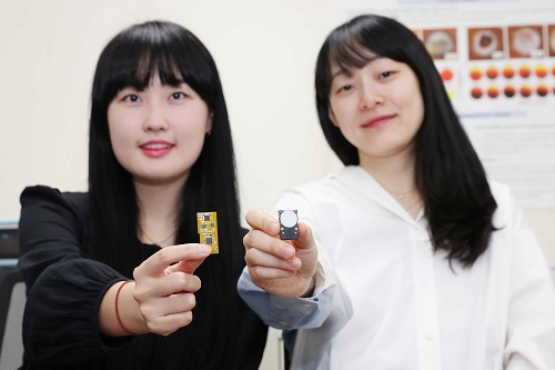
< Photo 1. (From left) Professor Inkyu Park of KAIST Department of Mechanical Engineering (ME), Dr. Jungrak Choi of ETRI, Ph.D. Candidate Donho Lee and M.S. Graduate Chankyu Han of KAIST ME >
When a robot grabs an object or a medical device detects a pulse, the tactile sensor is the technology that senses pressure like a fingertip. Existing sensors had disadvantages, such as slow responses or declining accuracy after repeated use, but Korean researchers have succeeded in developing a sensor that can quickly and accurately detect even light breath, pressure, and sound. This sensor can be used across a broad range — from everyday movements to medical diagnostics.
KAIST (represented by President Kwang Hyung Lee) announced on the 23rd of June that Professor Inkyu Park’s team from the Department of Mechanical Engineering, through a collaborative research project with the Electronics and Telecommunications Research Institute (ETRI, President Seung Chan Bang ) under the National Research Council of Science & Technology (NST, Chairman Young Sik Kim), has developed an innovative technology that overcomes the structural limitations of existing tactile sensors.
The core of this joint research is the implementation of a customized tactile sensor that simultaneously achieves flexibility, precision, and repeatable durability by applying Thermoformed 3D Electronics (T3DE).
< Figure 1. Comparative evaluation of soft elastomer–based 3D structure versus thermoforming-based 3D structure in terms of mechanical properties. >
In particular, soft elastomer-based sensors (rubber, silicone, etc. — materials that stretch and return to their original shape) have structural problems such as slow response times, high hysteresis*, and creep**, but this new platform operates precisely in diverse environments and overcomes these limitations.
*Hysteresis: A phenomenon where the previously applied force or change is retained like a “memory,” so that the same stimulus does not always produce the same result.
**Creep: The phenomenon where a material slowly deforms when a force is continuously applied.
T3DE sensors are manufactured by precisely forming electrodes on a 2D film, then thermoforming them into a 3D structure under heat and pressure. Specifically, the top electrodes and supporting pillar structures of the sensor are designed to allow the fine-tuning of the mechanical properties for different purposes. By adjusting microstructural parameters — such as the thickness, length, and number of support pillars — the sensor’s Young’s modulus* can be tuned across a broad range of 10 Pa to 1 MPa. This matches the stiffness of biological tissues like skin, muscle, and tendons, making them highly suitable as bio-interface sensors.
*Young’s modulus: An index representing a material's stiffness; this research can control this index to match various biological tissues.
The newly developed T3DE sensor uses air as a dielectric material to reduce power consumption and demonstrates outstanding performance in sensitivity, response time, thermal stability, and repeatable accuracy.
Experimental results showed that the sensor achieved △sensitivity of 5,884 kPa⁻¹, △response time of 0.1 ms (less than one-thousandth of a second), △hysteresis of less than 0.5%, and maintained a repeatable precision of 99.9% or higher even after 5,000 repeated measurements.
< Figure 2. Graphic Overview of thermoformed 3D electronics (T3DE) >
The research team also constructed a high-resolution 40×70 array, comprising a total of 2,800 densely packed sensors, to visualize the pressure distribution on the sole of the foot in real time during exercise and confirmed the possibility of using the sensor for wrist pulse measurement to assess vascular health. Furthermore, successful results were also achieved in sound-detection experiments at a level comparable to commercial acoustic sensors. In short, the sensor can precisely and quickly measure foot pressure, pulse, and sound, allowing it to be applied in areas such as sports, health, and sound sensing.
The T3DE technology was also applied to an augmented-reality(AR)-based surgical training system. By adjusting the stiffness of each sensor element to match that of biological tissues, the system provided real-time visual and tactile feedback according to the pressure applied during surgical incisions. It also offered real-time warnings if an incision was too deep or approached a risky area, making it a promising technology for enhancing immersion and accuracy in medical training.
KAIST Professor Inkyu Park stated, “Because this sensor can be precisely tuned from the design stage and operates reliably across diverse environments, it can be used not only in everyday life, but also in a variety of fields such as healthcare, rehabilitation, and virtual reality.”
The research was co-led as first authors by Dr. Jungrak Choi of ETRI, KAIST master’s student Chankyu Han, and Ph.D. candidate Donho Lee, under the overall guidance of Professor Inkyu Park. The research results were published in the May 2025 issue of ‘Science Advances’ and introduced to the global research community through the journal’s official SNS channels (Facebook, Twitter).
※ Thesis Title: Thermoforming 2D films into 3D electronics for high-performance, customizable tactile sensing
※ DOI: 10.1126/sciadv.adv0057
< Figure 3. The introduction of the study on the official SNS posting by Science Advances >
This research was supported by the Ministry of Trade, Industry and Energy, the National Research Foundation of Korea, and the Korea Institute for Advancement of Technology.
2025.06.23 View 7648
KAIST Develops Customized Tactile Sensor That Can Detect Light Breath, Pressure and Sound
< Photo 1. (From left) Professor Inkyu Park of KAIST Department of Mechanical Engineering (ME), Dr. Jungrak Choi of ETRI, Ph.D. Candidate Donho Lee and M.S. Graduate Chankyu Han of KAIST ME >
When a robot grabs an object or a medical device detects a pulse, the tactile sensor is the technology that senses pressure like a fingertip. Existing sensors had disadvantages, such as slow responses or declining accuracy after repeated use, but Korean researchers have succeeded in developing a sensor that can quickly and accurately detect even light breath, pressure, and sound. This sensor can be used across a broad range — from everyday movements to medical diagnostics.
KAIST (represented by President Kwang Hyung Lee) announced on the 23rd of June that Professor Inkyu Park’s team from the Department of Mechanical Engineering, through a collaborative research project with the Electronics and Telecommunications Research Institute (ETRI, President Seung Chan Bang ) under the National Research Council of Science & Technology (NST, Chairman Young Sik Kim), has developed an innovative technology that overcomes the structural limitations of existing tactile sensors.
The core of this joint research is the implementation of a customized tactile sensor that simultaneously achieves flexibility, precision, and repeatable durability by applying Thermoformed 3D Electronics (T3DE).
< Figure 1. Comparative evaluation of soft elastomer–based 3D structure versus thermoforming-based 3D structure in terms of mechanical properties. >
In particular, soft elastomer-based sensors (rubber, silicone, etc. — materials that stretch and return to their original shape) have structural problems such as slow response times, high hysteresis*, and creep**, but this new platform operates precisely in diverse environments and overcomes these limitations.
*Hysteresis: A phenomenon where the previously applied force or change is retained like a “memory,” so that the same stimulus does not always produce the same result.
**Creep: The phenomenon where a material slowly deforms when a force is continuously applied.
T3DE sensors are manufactured by precisely forming electrodes on a 2D film, then thermoforming them into a 3D structure under heat and pressure. Specifically, the top electrodes and supporting pillar structures of the sensor are designed to allow the fine-tuning of the mechanical properties for different purposes. By adjusting microstructural parameters — such as the thickness, length, and number of support pillars — the sensor’s Young’s modulus* can be tuned across a broad range of 10 Pa to 1 MPa. This matches the stiffness of biological tissues like skin, muscle, and tendons, making them highly suitable as bio-interface sensors.
*Young’s modulus: An index representing a material's stiffness; this research can control this index to match various biological tissues.
The newly developed T3DE sensor uses air as a dielectric material to reduce power consumption and demonstrates outstanding performance in sensitivity, response time, thermal stability, and repeatable accuracy.
Experimental results showed that the sensor achieved △sensitivity of 5,884 kPa⁻¹, △response time of 0.1 ms (less than one-thousandth of a second), △hysteresis of less than 0.5%, and maintained a repeatable precision of 99.9% or higher even after 5,000 repeated measurements.
< Figure 2. Graphic Overview of thermoformed 3D electronics (T3DE) >
The research team also constructed a high-resolution 40×70 array, comprising a total of 2,800 densely packed sensors, to visualize the pressure distribution on the sole of the foot in real time during exercise and confirmed the possibility of using the sensor for wrist pulse measurement to assess vascular health. Furthermore, successful results were also achieved in sound-detection experiments at a level comparable to commercial acoustic sensors. In short, the sensor can precisely and quickly measure foot pressure, pulse, and sound, allowing it to be applied in areas such as sports, health, and sound sensing.
The T3DE technology was also applied to an augmented-reality(AR)-based surgical training system. By adjusting the stiffness of each sensor element to match that of biological tissues, the system provided real-time visual and tactile feedback according to the pressure applied during surgical incisions. It also offered real-time warnings if an incision was too deep or approached a risky area, making it a promising technology for enhancing immersion and accuracy in medical training.
KAIST Professor Inkyu Park stated, “Because this sensor can be precisely tuned from the design stage and operates reliably across diverse environments, it can be used not only in everyday life, but also in a variety of fields such as healthcare, rehabilitation, and virtual reality.”
The research was co-led as first authors by Dr. Jungrak Choi of ETRI, KAIST master’s student Chankyu Han, and Ph.D. candidate Donho Lee, under the overall guidance of Professor Inkyu Park. The research results were published in the May 2025 issue of ‘Science Advances’ and introduced to the global research community through the journal’s official SNS channels (Facebook, Twitter).
※ Thesis Title: Thermoforming 2D films into 3D electronics for high-performance, customizable tactile sensing
※ DOI: 10.1126/sciadv.adv0057
< Figure 3. The introduction of the study on the official SNS posting by Science Advances >
This research was supported by the Ministry of Trade, Industry and Energy, the National Research Foundation of Korea, and the Korea Institute for Advancement of Technology.
2025.06.23 View 7648 -
 KAIST Succeeds in Real-Time Carbon Dioxide Monitoring Without Batteries or External Power
< (From left) Master's Student Gyurim Jang, Professor Kyeongha Kwon >
KAIST (President Kwang Hyung Lee) announced on June 9th that a research team led by Professor Kyeongha Kwon from the School of Electrical Engineering, in a joint study with Professor Hanjun Ryu's team at Chung-Ang University, has developed a self-powered wireless carbon dioxide (CO2) monitoring system. This innovative system harvests fine vibrational energy from its surroundings to periodically measure CO2 concentrations.
This breakthrough addresses a critical need in environmental monitoring: accurately understanding "how much" CO2 is being emitted to combat climate change and global warming. While CO2 monitoring technology is key to this, existing systems largely rely on batteries or wired power system, imposing limitations on installation and maintenance. The KAIST team tackled this by creating a self-powered wireless system that operates without external power.
The core of this new system is an "Inertia-driven Triboelectric Nanogenerator (TENG)" that converts vibrations (with amplitudes ranging from 20-4000 ㎛ and frequencies from 0-300 Hz) generated by industrial equipment or pipelines into electricity. This enables periodic CO2 concentration measurements and wireless transmission without the need for batteries.
< Figure 1. Concept and configuration of self-powered wireless CO2 monitoring system using fine vibration harvesting (a) System block diagram (b) Photo of fabricated system prototype >
The research team successfully amplified fine vibrations and induced resonance by combining spring-attached 4-stack TENGs. They achieved stable power production of 0.5 mW under conditions of 13 Hz and 0.56 g acceleration. The generated power was then used to operate a CO2 sensor and a Bluetooth Low Energy (BLE) system-on-a-chip (SoC).
Professor Kyeongha Kwon emphasized, "For efficient environmental monitoring, a system that can operate continuously without power limitations is essential." She explained, "In this research, we implemented a self-powered system that can periodically measure and wirelessly transmit CO2 concentrations based on the energy generated from an inertia-driven TENG." She added, "This technology can serve as a foundational technology for future self-powered environmental monitoring platforms integrating various sensors."
< Figure 2. TENG energy harvesting-based wireless CO2 sensing system operation results (c) Experimental setup (d) Measured CO2 concentration results powered by TENG and conventional DC power source >
This research was published on June 1st in the internationally renowned academic journal `Nano Energy (IF 16.8)`. Gyurim Jang, a master's student at KAIST, and Daniel Manaye Tiruneh, a master's student at Chung-Ang University, are the co-first authors of the paper.*Paper Title: Highly compact inertia-driven triboelectric nanogenerator for self-powered wireless CO2 monitoring via fine-vibration harvesting*DOI: 10.1016/j.nanoen.2025.110872
This research was supported by the Saudi Aramco-KAIST CO2 Management Center.
2025.06.09 View 55905
KAIST Succeeds in Real-Time Carbon Dioxide Monitoring Without Batteries or External Power
< (From left) Master's Student Gyurim Jang, Professor Kyeongha Kwon >
KAIST (President Kwang Hyung Lee) announced on June 9th that a research team led by Professor Kyeongha Kwon from the School of Electrical Engineering, in a joint study with Professor Hanjun Ryu's team at Chung-Ang University, has developed a self-powered wireless carbon dioxide (CO2) monitoring system. This innovative system harvests fine vibrational energy from its surroundings to periodically measure CO2 concentrations.
This breakthrough addresses a critical need in environmental monitoring: accurately understanding "how much" CO2 is being emitted to combat climate change and global warming. While CO2 monitoring technology is key to this, existing systems largely rely on batteries or wired power system, imposing limitations on installation and maintenance. The KAIST team tackled this by creating a self-powered wireless system that operates without external power.
The core of this new system is an "Inertia-driven Triboelectric Nanogenerator (TENG)" that converts vibrations (with amplitudes ranging from 20-4000 ㎛ and frequencies from 0-300 Hz) generated by industrial equipment or pipelines into electricity. This enables periodic CO2 concentration measurements and wireless transmission without the need for batteries.
< Figure 1. Concept and configuration of self-powered wireless CO2 monitoring system using fine vibration harvesting (a) System block diagram (b) Photo of fabricated system prototype >
The research team successfully amplified fine vibrations and induced resonance by combining spring-attached 4-stack TENGs. They achieved stable power production of 0.5 mW under conditions of 13 Hz and 0.56 g acceleration. The generated power was then used to operate a CO2 sensor and a Bluetooth Low Energy (BLE) system-on-a-chip (SoC).
Professor Kyeongha Kwon emphasized, "For efficient environmental monitoring, a system that can operate continuously without power limitations is essential." She explained, "In this research, we implemented a self-powered system that can periodically measure and wirelessly transmit CO2 concentrations based on the energy generated from an inertia-driven TENG." She added, "This technology can serve as a foundational technology for future self-powered environmental monitoring platforms integrating various sensors."
< Figure 2. TENG energy harvesting-based wireless CO2 sensing system operation results (c) Experimental setup (d) Measured CO2 concentration results powered by TENG and conventional DC power source >
This research was published on June 1st in the internationally renowned academic journal `Nano Energy (IF 16.8)`. Gyurim Jang, a master's student at KAIST, and Daniel Manaye Tiruneh, a master's student at Chung-Ang University, are the co-first authors of the paper.*Paper Title: Highly compact inertia-driven triboelectric nanogenerator for self-powered wireless CO2 monitoring via fine-vibration harvesting*DOI: 10.1016/j.nanoen.2025.110872
This research was supported by the Saudi Aramco-KAIST CO2 Management Center.
2025.06.09 View 55905 -
 KAIST Professor Jee-Hwan Ryu Receives Global IEEE Robotics Journal Best Paper Award
- Professor Jee-Hwan Ryu of Civil and Environmental Engineering receives the Best Paper Award from the Institute of Electrical and Electronics Engineers (IEEE) Robotics Journal, officially presented at ICRA, a world-renowned robotics conference.
- This is the highest level of international recognition, awarded to only the top 5 papers out of approximately 1,500 published in 2024.
- Securing a new working channel technology for soft growing robots expands the practicality and application possibilities in the field of soft robotics.
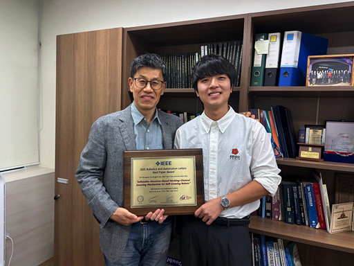
< Professor Jee-Hwan Ryu (left), Nam Gyun Kim, Ph.D. Candidate (right) from the KAIST Department of Civil and Environmental Engineering and KAIST Robotics Program >
KAIST (President Kwang-Hyung Lee) announced on the 6th that Professor Jee-Hwan Ryu from the Department of Civil and Environmental Engineering received the 2024 Best Paper Award from the Robotics and Automation Letters (RA-L), a premier journal under the IEEE, at the '2025 IEEE International Conference on Robotics and Automation (ICRA)' held in Atlanta, USA, on May 22nd.
This Best Paper Award is a prestigious honor presented to only the top 5 papers out of approximately 1,500 published in 2024, boasting high international competition and authority.
The award-winning paper by Professor Ryu proposes a novel working channel securing mechanism that significantly expands the practicality and application possibilities of 'Soft Growing Robots,' which are based on soft materials that move or perform tasks through a growing motion similar to plant roots.
< IEEE Robotics Journal Award Ceremony >
Existing soft growing robots move by inflating or contracting their bodies through increasing or decreasing internal pressure, which can lead to blockages in their internal passages. In contrast, the newly developed soft growing robot achieves a growing function while maintaining the internal passage pressure equal to the external atmospheric pressure, thereby successfully securing an internal passage while retaining the robot's flexible and soft characteristics.
This structure allows various materials or tools to be freely delivered through the internal passage (working channel) within the robot and offers the advantage of performing multi-purpose tasks by flexibly replacing equipment according to the working environment.
The research team fabricated a prototype to prove the effectiveness of this technology and verified its performance through various experiments. Specifically, in the slide plate experiment, they confirmed whether materials or equipment could pass through the robot's internal channel without obstruction, and in the pipe pulling experiment, they verified if a long pipe-shaped tool could be pulled through the internal channel.
< Figure 1. Overall hardware structure of the proposed soft growing robot (left) and a cross-sectional view composing the inflatable structure (right) >
Experimental results demonstrated that the internal channel remained stable even while the robot was growing, serving as a key basis for supporting the technology's practicality and scalability.
Professor Jee-Hwan Ryu stated, "This award is very meaningful as it signifies the global recognition of Korea's robotics technology and academic achievements. Especially, it holds great significance in achieving technical progress that can greatly expand the practicality and application fields of soft growing robots. This achievement was possible thanks to the dedication and collaboration of the research team, and I will continue to contribute to the development of robotics technology through innovative research."
< Figure 2. Material supplying mechanism of the Soft Growing Robot >
This research was co-authored by Dongoh Seo, Ph.D. Candidate in Civil and Environmental Engineering, and Nam Gyun Kim, Ph.D. Candidate in Robotics. It was published in IEEE Robotics and Automation Letters on September 1, 2024.
(Paper Title: Inflatable-Structure-Based Working-Channel Securing Mechanism for Soft Growing Robots, DOI: 10.1109/LRA.2024.3426322)
This project was supported simultaneously by the National Research Foundation of Korea's Future Promising Convergence Technology Pioneer Research Project and Mid-career Researcher Project.
2025.06.09 View 10069
KAIST Professor Jee-Hwan Ryu Receives Global IEEE Robotics Journal Best Paper Award
- Professor Jee-Hwan Ryu of Civil and Environmental Engineering receives the Best Paper Award from the Institute of Electrical and Electronics Engineers (IEEE) Robotics Journal, officially presented at ICRA, a world-renowned robotics conference.
- This is the highest level of international recognition, awarded to only the top 5 papers out of approximately 1,500 published in 2024.
- Securing a new working channel technology for soft growing robots expands the practicality and application possibilities in the field of soft robotics.
< Professor Jee-Hwan Ryu (left), Nam Gyun Kim, Ph.D. Candidate (right) from the KAIST Department of Civil and Environmental Engineering and KAIST Robotics Program >
KAIST (President Kwang-Hyung Lee) announced on the 6th that Professor Jee-Hwan Ryu from the Department of Civil and Environmental Engineering received the 2024 Best Paper Award from the Robotics and Automation Letters (RA-L), a premier journal under the IEEE, at the '2025 IEEE International Conference on Robotics and Automation (ICRA)' held in Atlanta, USA, on May 22nd.
This Best Paper Award is a prestigious honor presented to only the top 5 papers out of approximately 1,500 published in 2024, boasting high international competition and authority.
The award-winning paper by Professor Ryu proposes a novel working channel securing mechanism that significantly expands the practicality and application possibilities of 'Soft Growing Robots,' which are based on soft materials that move or perform tasks through a growing motion similar to plant roots.
< IEEE Robotics Journal Award Ceremony >
Existing soft growing robots move by inflating or contracting their bodies through increasing or decreasing internal pressure, which can lead to blockages in their internal passages. In contrast, the newly developed soft growing robot achieves a growing function while maintaining the internal passage pressure equal to the external atmospheric pressure, thereby successfully securing an internal passage while retaining the robot's flexible and soft characteristics.
This structure allows various materials or tools to be freely delivered through the internal passage (working channel) within the robot and offers the advantage of performing multi-purpose tasks by flexibly replacing equipment according to the working environment.
The research team fabricated a prototype to prove the effectiveness of this technology and verified its performance through various experiments. Specifically, in the slide plate experiment, they confirmed whether materials or equipment could pass through the robot's internal channel without obstruction, and in the pipe pulling experiment, they verified if a long pipe-shaped tool could be pulled through the internal channel.
< Figure 1. Overall hardware structure of the proposed soft growing robot (left) and a cross-sectional view composing the inflatable structure (right) >
Experimental results demonstrated that the internal channel remained stable even while the robot was growing, serving as a key basis for supporting the technology's practicality and scalability.
Professor Jee-Hwan Ryu stated, "This award is very meaningful as it signifies the global recognition of Korea's robotics technology and academic achievements. Especially, it holds great significance in achieving technical progress that can greatly expand the practicality and application fields of soft growing robots. This achievement was possible thanks to the dedication and collaboration of the research team, and I will continue to contribute to the development of robotics technology through innovative research."
< Figure 2. Material supplying mechanism of the Soft Growing Robot >
This research was co-authored by Dongoh Seo, Ph.D. Candidate in Civil and Environmental Engineering, and Nam Gyun Kim, Ph.D. Candidate in Robotics. It was published in IEEE Robotics and Automation Letters on September 1, 2024.
(Paper Title: Inflatable-Structure-Based Working-Channel Securing Mechanism for Soft Growing Robots, DOI: 10.1109/LRA.2024.3426322)
This project was supported simultaneously by the National Research Foundation of Korea's Future Promising Convergence Technology Pioneer Research Project and Mid-career Researcher Project.
2025.06.09 View 10069 -
 KAIST Innovates Mid-Infrared Photodetectors for Exoplanet Detection, Expanding Applications to Environmental and Medical Fields
NASA’s James Webb Space Telescope (JWST) utilizes mid-infrared spectroscopy to precisely analyze molecular components such as water vapor and sulfur dioxide in exoplanet atmospheres. The key to this analysis, where each molecule exhibits a unique spectral "fingerprint," lies in highly sensitive photodetector technology capable of measuring extremely weak light intensities. Recently, KAIST researchers have developed an innovative photodetector capable of detecting a broad range of mid-infrared spectra, garnering significant attention.
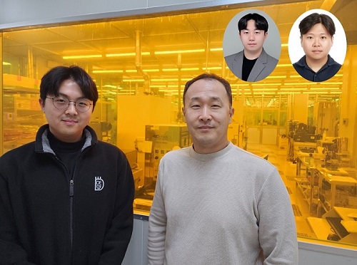
< Photo 1. (from the left) Ph.D. candidate Inki Kim (co-author), Professor SangHyeon Kim (corresponding author), Dr. Joonsup Shim (first author), and Dr. Jinha Lim (co-author) of KAIST School of Electrical Engineering. >
KAIST (represented by President Kwang-Hyung Lee) announced on the 27th of March that a research team led by Professor SangHyeon Kim from the School of Electrical Engineering has developed a mid-infrared photodetector that operates stably at room temperature, marking a major turning point for the commercialization of ultra-compact optical sensors.
The newly developed photodetector utilizes conventional silicon-based CMOS processes, enabling low-cost mass production while maintaining stable operation at room temperature. Notably, the research team successfully demonstrated the real-time detection of carbon dioxide (CO₂) gas using ultra-compact and ultra-thin optical sensors equipped with this photodetector, proving its potential for environmental monitoring and hazardous gas analysis.
Existing mid-infrared photodetectors generally require cooling systems due to high thermal noise at room temperature. These cooling systems increase the size and cost of equipment, making miniaturization and integration into portable devices challenging. Furthermore, conventional mid-infrared photodetectors are incompatible with silicon-based CMOS processes, limiting large-scale production and commercialization.
To address these limitations, the research team developed a waveguide-integrated photodetector using germanium (Ge), a Group IV element like silicon. This approach enables broad-spectrum mid-infrared detection while ensuring stable operation at room temperature.
< Figure 1. Schematic diagram of a room-temperature mid-infrared waveguide-integrated photodetector based on the Ge-on-insulator optical platform proposed in this study (top). Optical microscope image of the integrated photodetector connected with the sensing unit (bottom). >
A waveguide is a structure designed to efficiently guide light along a specific path with minimal loss. To implement various optical functions on a chip (on-chip), the development of waveguide-integrated photodetectors and waveguide-based optical components is essential.
Unlike conventional photodetectors that primarily rely on bandgap absorption principles, this new technology leverages the bolometric effect*, allowing it to detect the entire mid-infrared spectral range. As a result, it can be widely applied to the real-time sensing of various molecular species.
*Bolometric effect: A principle in which light absorption leads to an increase in temperature, causing electrical signals to change accordingly.
The waveguide-integrated mid-infrared photodetector developed by the research team is considered a groundbreaking innovation that overcomes the limitations of existing mid-infrared sensor technologies, including the need for cooling, difficulties in mass production, and high costs.
< Figure 2. Room temperature photoresponse characteristics of the mid-infrared waveguide photodetector proposed in this study (left) and real-time carbon dioxide (CO2) gas sensing results using the photodetector (right). >
This breakthrough technology is expected to be applicable across diverse fields, including environmental monitoring, medical diagnostics, industrial process management, national defense and security, and smart devices. It also paves the way for next-generation mid-infrared sensor advancements.
Professor SangHyeon Kim from KAIST stated, "This research represents a novel approach that overcomes the limitations of existing mid-infrared photodetector technologies and has great potential for practical applications in various fields." He further emphasized, "Since this sensor technology is compatible with CMOS processes, it enables low-cost mass production, making it highly suitable for next-generation environmental monitoring systems and smart manufacturing sites."
< Figure 3. Performance comparison image of a room-temperature mid-infrared waveguide photodetector fabricated with the technology proposed in this study. It achieves the world’s highest performance compared to existing technologies utilizing the Bolometric effect, and is the only solution compatible with CMOS processes. The technology proposed by our research team is characterized by its ability to respond to a wide spectrum of the mid-infrared band without limitations. >
The study, with Dr. Joonsup Shim (currently a postdoctoral researcher at Harvard University) as the first author, was published on March 19, 2025 in the internationally renowned journal Light: Science & Applications (JCR 2.9%, IF=20.6).
(Paper title: “Room-temperature waveguide-integrated photodetector using bolometric effect for mid-infrared spectroscopy applications,” https://doi.org/10.1038/s41377-025-01803-3)
2025.03.27 View 8939
KAIST Innovates Mid-Infrared Photodetectors for Exoplanet Detection, Expanding Applications to Environmental and Medical Fields
NASA’s James Webb Space Telescope (JWST) utilizes mid-infrared spectroscopy to precisely analyze molecular components such as water vapor and sulfur dioxide in exoplanet atmospheres. The key to this analysis, where each molecule exhibits a unique spectral "fingerprint," lies in highly sensitive photodetector technology capable of measuring extremely weak light intensities. Recently, KAIST researchers have developed an innovative photodetector capable of detecting a broad range of mid-infrared spectra, garnering significant attention.
< Photo 1. (from the left) Ph.D. candidate Inki Kim (co-author), Professor SangHyeon Kim (corresponding author), Dr. Joonsup Shim (first author), and Dr. Jinha Lim (co-author) of KAIST School of Electrical Engineering. >
KAIST (represented by President Kwang-Hyung Lee) announced on the 27th of March that a research team led by Professor SangHyeon Kim from the School of Electrical Engineering has developed a mid-infrared photodetector that operates stably at room temperature, marking a major turning point for the commercialization of ultra-compact optical sensors.
The newly developed photodetector utilizes conventional silicon-based CMOS processes, enabling low-cost mass production while maintaining stable operation at room temperature. Notably, the research team successfully demonstrated the real-time detection of carbon dioxide (CO₂) gas using ultra-compact and ultra-thin optical sensors equipped with this photodetector, proving its potential for environmental monitoring and hazardous gas analysis.
Existing mid-infrared photodetectors generally require cooling systems due to high thermal noise at room temperature. These cooling systems increase the size and cost of equipment, making miniaturization and integration into portable devices challenging. Furthermore, conventional mid-infrared photodetectors are incompatible with silicon-based CMOS processes, limiting large-scale production and commercialization.
To address these limitations, the research team developed a waveguide-integrated photodetector using germanium (Ge), a Group IV element like silicon. This approach enables broad-spectrum mid-infrared detection while ensuring stable operation at room temperature.
< Figure 1. Schematic diagram of a room-temperature mid-infrared waveguide-integrated photodetector based on the Ge-on-insulator optical platform proposed in this study (top). Optical microscope image of the integrated photodetector connected with the sensing unit (bottom). >
A waveguide is a structure designed to efficiently guide light along a specific path with minimal loss. To implement various optical functions on a chip (on-chip), the development of waveguide-integrated photodetectors and waveguide-based optical components is essential.
Unlike conventional photodetectors that primarily rely on bandgap absorption principles, this new technology leverages the bolometric effect*, allowing it to detect the entire mid-infrared spectral range. As a result, it can be widely applied to the real-time sensing of various molecular species.
*Bolometric effect: A principle in which light absorption leads to an increase in temperature, causing electrical signals to change accordingly.
The waveguide-integrated mid-infrared photodetector developed by the research team is considered a groundbreaking innovation that overcomes the limitations of existing mid-infrared sensor technologies, including the need for cooling, difficulties in mass production, and high costs.
< Figure 2. Room temperature photoresponse characteristics of the mid-infrared waveguide photodetector proposed in this study (left) and real-time carbon dioxide (CO2) gas sensing results using the photodetector (right). >
This breakthrough technology is expected to be applicable across diverse fields, including environmental monitoring, medical diagnostics, industrial process management, national defense and security, and smart devices. It also paves the way for next-generation mid-infrared sensor advancements.
Professor SangHyeon Kim from KAIST stated, "This research represents a novel approach that overcomes the limitations of existing mid-infrared photodetector technologies and has great potential for practical applications in various fields." He further emphasized, "Since this sensor technology is compatible with CMOS processes, it enables low-cost mass production, making it highly suitable for next-generation environmental monitoring systems and smart manufacturing sites."
< Figure 3. Performance comparison image of a room-temperature mid-infrared waveguide photodetector fabricated with the technology proposed in this study. It achieves the world’s highest performance compared to existing technologies utilizing the Bolometric effect, and is the only solution compatible with CMOS processes. The technology proposed by our research team is characterized by its ability to respond to a wide spectrum of the mid-infrared band without limitations. >
The study, with Dr. Joonsup Shim (currently a postdoctoral researcher at Harvard University) as the first author, was published on March 19, 2025 in the internationally renowned journal Light: Science & Applications (JCR 2.9%, IF=20.6).
(Paper title: “Room-temperature waveguide-integrated photodetector using bolometric effect for mid-infrared spectroscopy applications,” https://doi.org/10.1038/s41377-025-01803-3)
2025.03.27 View 8939 -
 No More Touch Issues on Rainy Days! KAIST Develops Human-Like Tactile Sensor
Recent advancements in robotics have enabled machines to handle delicate objects like eggs with precision, thanks to highly integrated pressure sensors that provide detailed tactile feedback. However, even the most advanced robots struggle to accurately detect pressure in complex environments involving water, bending, or electromagnetic interference. A research team at KAIST has successfully developed a pressure sensor that operates stably without external interference, even on wet surfaces like a smartphone screen covered in water, achieving human-level tactile sensitivity.
KAIST (represented by President Kwang Hyung Lee) announced on the 10th of March that a research team led by Professor Jun-Bo Yoon from the School of Electrical Engineering has developed a high-resolution pressure sensor that remains unaffected by external interference such as "ghost touches" caused by moisture on touchscreens.
Capacitive pressure sensors, widely used in touch systems due to their simple structure and durability, are essential components of human-machine interface (HMI) technologies in smartphones, wearable devices, and robots. However, they are prone to malfunctions caused by water droplets, electromagnetic interference, and curves.
To address these issues, the research team investigated the root causes of interference in capacitive pressure sensors. They identified that the "fringe field" generated at the sensor’s edges is particularly susceptible to external disturbances.
The researchers concluded that, to fundamentally resolve this issue, suppressing the fringe field was necessary. Through theoretical analysis, they determined that reducing the electrode spacing to the nanometer scale could effectively minimize the fringe field to below a few percent.
Utilizing proprietary micro/nanofabrication techniques, the team developed a nanogap pressure sensor with an electrode spacing of 900 nanometers (nm). This newly developed sensor reliably detected pressure regardless of the material exerting force and remained unaffected by bending or electromagnetic interference.
Furthermore, the team successfully implemented an artificial tactile system utilizing the developed sensor’s characteristics. Human skin contains specialized pressure receptors called Merkel’s disks. To artificially mimic them, the exclusive detection of pressure was necessary, but hadn’t been achieved by conventional sensors.
Professor Yoon’s research team overcame these challenges, developing a sensor achieving a density comparable to Merkel’s discs and enabling wireless, high-precision pressure sensing.
To explore potential applications, the researcher also developed a force touch pad system, demonstrating its ability to capture pressure magnitude and distribution with high resolution and without interference.
Professor Yoon stated, “Our nanogap pressure sensor operates reliably even in rainy conditions or sweaty environments, eliminating common touch malfunctions. We believe this innovation will significantly enhance everyday user experiences.”
He added, “This technology has the potential to revolutionize various fields, including precision tactile sensors for robotics, medical wearable devices, and next-generation augmented reality (AR) and virtual reality (VR) interfaces.”
The study was led by Jae-Soon Yang (Ph.D.), Myung-Kun Chung (Ph.D. candidate), and Jae-Young Yoo (Assistant Professor at Sungkyunkwan University, a KAIST Ph.D. graduate). The research findings were published in Nature Communications on February 27, 2025. (Paper title: “Interference-Free Nanogap Pressure Sensor Array with High Spatial Resolution for Wireless Human-Machine Interface Applications”, DOI: 10.1038/s41467-025-57232-8)
This study was supported by the National Research Foundation of Korea’s Mid-Career Researcher Program and Leading Research Center Support Program.
2025.03.14 View 8539
No More Touch Issues on Rainy Days! KAIST Develops Human-Like Tactile Sensor
Recent advancements in robotics have enabled machines to handle delicate objects like eggs with precision, thanks to highly integrated pressure sensors that provide detailed tactile feedback. However, even the most advanced robots struggle to accurately detect pressure in complex environments involving water, bending, or electromagnetic interference. A research team at KAIST has successfully developed a pressure sensor that operates stably without external interference, even on wet surfaces like a smartphone screen covered in water, achieving human-level tactile sensitivity.
KAIST (represented by President Kwang Hyung Lee) announced on the 10th of March that a research team led by Professor Jun-Bo Yoon from the School of Electrical Engineering has developed a high-resolution pressure sensor that remains unaffected by external interference such as "ghost touches" caused by moisture on touchscreens.
Capacitive pressure sensors, widely used in touch systems due to their simple structure and durability, are essential components of human-machine interface (HMI) technologies in smartphones, wearable devices, and robots. However, they are prone to malfunctions caused by water droplets, electromagnetic interference, and curves.
To address these issues, the research team investigated the root causes of interference in capacitive pressure sensors. They identified that the "fringe field" generated at the sensor’s edges is particularly susceptible to external disturbances.
The researchers concluded that, to fundamentally resolve this issue, suppressing the fringe field was necessary. Through theoretical analysis, they determined that reducing the electrode spacing to the nanometer scale could effectively minimize the fringe field to below a few percent.
Utilizing proprietary micro/nanofabrication techniques, the team developed a nanogap pressure sensor with an electrode spacing of 900 nanometers (nm). This newly developed sensor reliably detected pressure regardless of the material exerting force and remained unaffected by bending or electromagnetic interference.
Furthermore, the team successfully implemented an artificial tactile system utilizing the developed sensor’s characteristics. Human skin contains specialized pressure receptors called Merkel’s disks. To artificially mimic them, the exclusive detection of pressure was necessary, but hadn’t been achieved by conventional sensors.
Professor Yoon’s research team overcame these challenges, developing a sensor achieving a density comparable to Merkel’s discs and enabling wireless, high-precision pressure sensing.
To explore potential applications, the researcher also developed a force touch pad system, demonstrating its ability to capture pressure magnitude and distribution with high resolution and without interference.
Professor Yoon stated, “Our nanogap pressure sensor operates reliably even in rainy conditions or sweaty environments, eliminating common touch malfunctions. We believe this innovation will significantly enhance everyday user experiences.”
He added, “This technology has the potential to revolutionize various fields, including precision tactile sensors for robotics, medical wearable devices, and next-generation augmented reality (AR) and virtual reality (VR) interfaces.”
The study was led by Jae-Soon Yang (Ph.D.), Myung-Kun Chung (Ph.D. candidate), and Jae-Young Yoo (Assistant Professor at Sungkyunkwan University, a KAIST Ph.D. graduate). The research findings were published in Nature Communications on February 27, 2025. (Paper title: “Interference-Free Nanogap Pressure Sensor Array with High Spatial Resolution for Wireless Human-Machine Interface Applications”, DOI: 10.1038/s41467-025-57232-8)
This study was supported by the National Research Foundation of Korea’s Mid-Career Researcher Program and Leading Research Center Support Program.
2025.03.14 View 8539 -
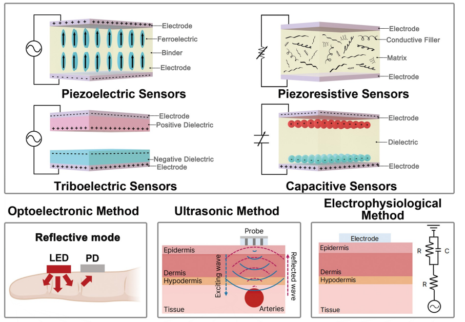 AI-Driven Wearable Blood Pressure Sensor for Continuous Health Monitoring – Published in Nature Reviews Cardiology
A KAIST research team led by Professor Keon Jae Lee has proposed an innovative theoretical framework and research strategies for AI-based wearable blood pressure sensors, paving the way for continuous and non-invasive cardiovascular monitoring.
Hypertension is a leading chronic disease affecting over a billion people worldwide and is a major risk factor for severe cardiovascular conditions such as myocardial infarction, stroke, and heart failure. Traditional blood pressure measurement relies on intermittent, cuff-based methods, which fail to capture real-time fluctuations and present challenges in continuous patient monitoring.
Wearable blood pressure sensors offer a non-invasive solution for continuous blood pressure monitoring, enabling real-time tracking and personalized cardiovascular health management. However, current technologies lack the accuracy and reliability required for medical applications, limiting their practical use. To address these challenges, advancements in high-sensitivity sensor technology and AI signal processing algorithms are essential.
Building on their previous study in Advanced Materials (doi.org/10.1002/adma.202301627), which validated the clinical feasibility of flexible piezoelectric blood pressure sensors, Professor Lee’s team conducted an in-depth review of the latest advancements in cuffless wearable sensors, focusing on key technical and clinical challenges. Their review highlights clinical aspects of clinical implementation, real-time data transmission, signal quality degradation, and AI algorithm accuracy.
Professor Keon Jae Lee said, “This paper systematically demonstrates the feasibility of medical-grade wearable blood pressure sensors, overcoming what was previously considered an insurmountable challenge. We propose theoretical strategies to address technical barriers, opening new possibilities for future innovations in this field. With continued advancements, we expect these sensors to gain trust and be commercialized soon, significantly improving quality of life.”
This review entitled “Wearable blood pressure sensors for cardiovascular monitoring and machine learning algorithms for blood pressure estimation” was published in the February 18 issue of Nature Reviews Cardiology (Impact Factor: 41.7). (doi.org/10.1038/s41569-025-01127-0)
< Figure 1. Overview of wearable blood pressure sensor technologies for cardiovascular health care >
[Reference] Min S. et al., (2025) “Wearable blood pressure sensors for
cardiovascular monitoring and machine learning algorithms for blood pressure estimation.” Nature Reviews Cardiology
(doi.org/10.1038/s41569-025-01127-0)
[Main Author] Seongwook Min (Korea Advanced Institute of Science and Technology), Jaehun An (Korea Advanced Institute of Science and Technology), Jae Hee Lee (Northwestern University),
* Contact email : Professor Keon Jae Lee (keonlee@kaist.ac.kr)
2025.03.04 View 10041
AI-Driven Wearable Blood Pressure Sensor for Continuous Health Monitoring – Published in Nature Reviews Cardiology
A KAIST research team led by Professor Keon Jae Lee has proposed an innovative theoretical framework and research strategies for AI-based wearable blood pressure sensors, paving the way for continuous and non-invasive cardiovascular monitoring.
Hypertension is a leading chronic disease affecting over a billion people worldwide and is a major risk factor for severe cardiovascular conditions such as myocardial infarction, stroke, and heart failure. Traditional blood pressure measurement relies on intermittent, cuff-based methods, which fail to capture real-time fluctuations and present challenges in continuous patient monitoring.
Wearable blood pressure sensors offer a non-invasive solution for continuous blood pressure monitoring, enabling real-time tracking and personalized cardiovascular health management. However, current technologies lack the accuracy and reliability required for medical applications, limiting their practical use. To address these challenges, advancements in high-sensitivity sensor technology and AI signal processing algorithms are essential.
Building on their previous study in Advanced Materials (doi.org/10.1002/adma.202301627), which validated the clinical feasibility of flexible piezoelectric blood pressure sensors, Professor Lee’s team conducted an in-depth review of the latest advancements in cuffless wearable sensors, focusing on key technical and clinical challenges. Their review highlights clinical aspects of clinical implementation, real-time data transmission, signal quality degradation, and AI algorithm accuracy.
Professor Keon Jae Lee said, “This paper systematically demonstrates the feasibility of medical-grade wearable blood pressure sensors, overcoming what was previously considered an insurmountable challenge. We propose theoretical strategies to address technical barriers, opening new possibilities for future innovations in this field. With continued advancements, we expect these sensors to gain trust and be commercialized soon, significantly improving quality of life.”
This review entitled “Wearable blood pressure sensors for cardiovascular monitoring and machine learning algorithms for blood pressure estimation” was published in the February 18 issue of Nature Reviews Cardiology (Impact Factor: 41.7). (doi.org/10.1038/s41569-025-01127-0)
< Figure 1. Overview of wearable blood pressure sensor technologies for cardiovascular health care >
[Reference] Min S. et al., (2025) “Wearable blood pressure sensors for
cardiovascular monitoring and machine learning algorithms for blood pressure estimation.” Nature Reviews Cardiology
(doi.org/10.1038/s41569-025-01127-0)
[Main Author] Seongwook Min (Korea Advanced Institute of Science and Technology), Jaehun An (Korea Advanced Institute of Science and Technology), Jae Hee Lee (Northwestern University),
* Contact email : Professor Keon Jae Lee (keonlee@kaist.ac.kr)
2025.03.04 View 10041 -
 KAIST Develops Wearable Carbon Dioxide Sensor to Enable Real-time Apnea Diagnosis
- Professor Seunghyup Yoo’s research team of the School of Electrical Engineering developed an ultralow-power carbon dioxide (CO2) sensor using a flexible and thin organic photodiode, and succeeded in real-time breathing monitoring by attaching it to a commercial mask
- Wearable devices with features such as low power, high stability, and flexibility can be utilized for early diagnosis of various diseases such as chronic obstructive pulmonary disease and sleep apnea
< Photo 1. From the left, School of Electrical Engineering, Ph.D. candidate DongHo Choi, Professor Seunghyup Yoo, and Department of Materials Science and Engineering, Bachelor’s candidate MinJae Kim >
Carbon dioxide (CO2) is a major respiratory metabolite, and continuous monitoring of CO2 concentration in exhaled breath is not only an important indicator for early detection and diagnosis of respiratory and circulatory system diseases, but can also be widely used for monitoring personal exercise status. KAIST researchers succeeded in accurately measuring CO2 concentration by attaching it to the inside of a mask.
KAIST (President Kwang-Hyung Lee) announced on February 10th that Professor Seunghyup Yoo's research team in the Department of Electrical and Electronic Engineering developed a low-power, high-speed wearable CO2 sensor capable of stable breathing monitoring in real time.
Existing non-invasive CO2 sensors had limitations in that they were large in size and consumed high power. In particular, optochemical CO2 sensors using fluorescent molecules have the advantage of being miniaturized and lightweight, but due to the photodegradation phenomenon of dye molecules, they are difficult to use stably for a long time, which limits their use as wearable healthcare sensors.
Optochemical CO2 sensors utilize the fact that the intensity of fluorescence emitted from fluorescent molecules decreases depending on the concentration of CO2, and it is important to effectively detect changes in fluorescence light.
To this end, the research team developed a low-power CO2 sensor consisting of an LED and an organic photodiode surrounding it. Based on high light collection efficiency, the sensor, which minimizes the amount of excitation light irradiated on fluorescent molecules, achieved a device power consumption of 171 μW, which is tens of times lower than existing sensors that consume several mW.
< Figure 1. Structure and operating principle of the developed optochemical carbon dioxide (CO2) sensor. Light emitted from the LED is converted into fluorescence through the fluorescent film, reflected from the light scattering layer, and incident on the organic photodiode. CO2 reacts with a small amount of water inside the fluorescent film to form carbonic acid (H2CO3), which increases the concentration of hydrogen ions (H+), and the fluorescence intensity due to 470 nm excitation light decreases. The circular organic photodiode with high light collection efficiency effectively detects changes in fluorescence intensity, lowers the power required light up the LED, and reduces light-induced deterioration. >
The research team also elucidated the photodegradation path of fluorescent molecules used in CO2 sensors, revealed the cause of the increase in error over time in photochemical sensors, and suggested an optical design method to suppress the occurrence of errors.
Based on this, the research team developed a sensor that effectively reduces errors caused by photodegradation, which was a chronic problem of existing photochemical sensors, and can be used continuously for up to 9 hours while existing technologies based on the same material can be used for less than 20 minutes, and can be used multiple times when replacing the CO2 detection fluorescent film.
< Figure 2. Wearable smart mask and real-time breathing monitoring. The fabricated sensor module consists of four elements (①: gas-permeable light-scattering layer, ②: color filter and organic photodiode, ③: light-emitting diode, ④: CO2-detecting fluorescent film). The thin and light sensor (D1: 400 nm, D2: 470 nm) is attached to the inside of the mask to monitor the wearer's breathing in real time. >
The developed sensor accurately measured CO2 concentration by being attached to the inside of a mask based on the advantages of being light (0.12 g), thin (0.7 mm), and flexible. In addition, it showed fast speed and high resolution that can monitor respiratory rate by distinguishing between inhalation and exhalation in real time.
< Photo 2. The developed sensor attached to the inside of the mask >
Professor Seunghyup Yoo said, "The developed sensor has excellent characteristics such as low power, high stability, and flexibility, so it can be widely applied to wearable devices, and can be used for the early diagnosis of various diseases such as hypercapnia, chronic obstructive pulmonary disease, and sleep apnea." He added, "In particular, it is expected to be used to improve side effects caused by rebreathing in environments where dust is generated or where masks are worn for long periods of time, such as during seasonal changes."
This study, in which KAIST's Department of Materials Science and Engineering's undergraduate student Minjae Kim and School of Electrical Engineering's doctoral student Dongho Choi participated as joint first authors, was published in the online version of Cell's sister journal, Device, on the 22nd of last month. (Paper title: Ultralow-power carbon dioxide sensor for real-time breath monitoring) DOI: https://doi.org/10.1016/j.device.2024.100681
< Photo 3. From the left, Professor Seunghyup Yoo of the School of Electrical Engineering, MinJae Kim, an undergraduate student in the Department of Materials Science and Engineering, and Dongho Choi, a doctoral student in the School of Electrical Engineering >
This study was supported by the Ministry of Trade, Industry and Energy's Materials and Components Technology Development Project, the National Research Foundation of Korea's Original Technology Development Project, and the KAIST Undergraduate Research Participation Project. This work was supported by the (URP) program.
2025.02.13 View 15941
KAIST Develops Wearable Carbon Dioxide Sensor to Enable Real-time Apnea Diagnosis
- Professor Seunghyup Yoo’s research team of the School of Electrical Engineering developed an ultralow-power carbon dioxide (CO2) sensor using a flexible and thin organic photodiode, and succeeded in real-time breathing monitoring by attaching it to a commercial mask
- Wearable devices with features such as low power, high stability, and flexibility can be utilized for early diagnosis of various diseases such as chronic obstructive pulmonary disease and sleep apnea
< Photo 1. From the left, School of Electrical Engineering, Ph.D. candidate DongHo Choi, Professor Seunghyup Yoo, and Department of Materials Science and Engineering, Bachelor’s candidate MinJae Kim >
Carbon dioxide (CO2) is a major respiratory metabolite, and continuous monitoring of CO2 concentration in exhaled breath is not only an important indicator for early detection and diagnosis of respiratory and circulatory system diseases, but can also be widely used for monitoring personal exercise status. KAIST researchers succeeded in accurately measuring CO2 concentration by attaching it to the inside of a mask.
KAIST (President Kwang-Hyung Lee) announced on February 10th that Professor Seunghyup Yoo's research team in the Department of Electrical and Electronic Engineering developed a low-power, high-speed wearable CO2 sensor capable of stable breathing monitoring in real time.
Existing non-invasive CO2 sensors had limitations in that they were large in size and consumed high power. In particular, optochemical CO2 sensors using fluorescent molecules have the advantage of being miniaturized and lightweight, but due to the photodegradation phenomenon of dye molecules, they are difficult to use stably for a long time, which limits their use as wearable healthcare sensors.
Optochemical CO2 sensors utilize the fact that the intensity of fluorescence emitted from fluorescent molecules decreases depending on the concentration of CO2, and it is important to effectively detect changes in fluorescence light.
To this end, the research team developed a low-power CO2 sensor consisting of an LED and an organic photodiode surrounding it. Based on high light collection efficiency, the sensor, which minimizes the amount of excitation light irradiated on fluorescent molecules, achieved a device power consumption of 171 μW, which is tens of times lower than existing sensors that consume several mW.
< Figure 1. Structure and operating principle of the developed optochemical carbon dioxide (CO2) sensor. Light emitted from the LED is converted into fluorescence through the fluorescent film, reflected from the light scattering layer, and incident on the organic photodiode. CO2 reacts with a small amount of water inside the fluorescent film to form carbonic acid (H2CO3), which increases the concentration of hydrogen ions (H+), and the fluorescence intensity due to 470 nm excitation light decreases. The circular organic photodiode with high light collection efficiency effectively detects changes in fluorescence intensity, lowers the power required light up the LED, and reduces light-induced deterioration. >
The research team also elucidated the photodegradation path of fluorescent molecules used in CO2 sensors, revealed the cause of the increase in error over time in photochemical sensors, and suggested an optical design method to suppress the occurrence of errors.
Based on this, the research team developed a sensor that effectively reduces errors caused by photodegradation, which was a chronic problem of existing photochemical sensors, and can be used continuously for up to 9 hours while existing technologies based on the same material can be used for less than 20 minutes, and can be used multiple times when replacing the CO2 detection fluorescent film.
< Figure 2. Wearable smart mask and real-time breathing monitoring. The fabricated sensor module consists of four elements (①: gas-permeable light-scattering layer, ②: color filter and organic photodiode, ③: light-emitting diode, ④: CO2-detecting fluorescent film). The thin and light sensor (D1: 400 nm, D2: 470 nm) is attached to the inside of the mask to monitor the wearer's breathing in real time. >
The developed sensor accurately measured CO2 concentration by being attached to the inside of a mask based on the advantages of being light (0.12 g), thin (0.7 mm), and flexible. In addition, it showed fast speed and high resolution that can monitor respiratory rate by distinguishing between inhalation and exhalation in real time.
< Photo 2. The developed sensor attached to the inside of the mask >
Professor Seunghyup Yoo said, "The developed sensor has excellent characteristics such as low power, high stability, and flexibility, so it can be widely applied to wearable devices, and can be used for the early diagnosis of various diseases such as hypercapnia, chronic obstructive pulmonary disease, and sleep apnea." He added, "In particular, it is expected to be used to improve side effects caused by rebreathing in environments where dust is generated or where masks are worn for long periods of time, such as during seasonal changes."
This study, in which KAIST's Department of Materials Science and Engineering's undergraduate student Minjae Kim and School of Electrical Engineering's doctoral student Dongho Choi participated as joint first authors, was published in the online version of Cell's sister journal, Device, on the 22nd of last month. (Paper title: Ultralow-power carbon dioxide sensor for real-time breath monitoring) DOI: https://doi.org/10.1016/j.device.2024.100681
< Photo 3. From the left, Professor Seunghyup Yoo of the School of Electrical Engineering, MinJae Kim, an undergraduate student in the Department of Materials Science and Engineering, and Dongho Choi, a doctoral student in the School of Electrical Engineering >
This study was supported by the Ministry of Trade, Industry and Energy's Materials and Components Technology Development Project, the National Research Foundation of Korea's Original Technology Development Project, and the KAIST Undergraduate Research Participation Project. This work was supported by the (URP) program.
2025.02.13 View 15941 -
 KAIST Secures Core Technology for Ultra-High-Resolution Image Sensors
A joint research team from Korea and the United States has developed next-generation, high-resolution image sensor technology with higher power efficiency and a smaller size compared to existing sensors. Notably, they have secured foundational technology for ultra-high-resolution shortwave infrared (SWIR) image sensors, an area currently dominated by Sony, paving the way for future market entry.
KAIST (represented by President Kwang Hyung Lee) announced on the 20th of November that a research team led by Professor SangHyeon Kim from the School of Electrical Engineering, in collaboration with Inha University and Yale University in the U.S., has developed an ultra-thin broadband photodiode (PD), marking a significant breakthrough in high-performance image sensor technology.
This research drastically improves the trade-off between the absorption layer thickness and quantum efficiency found in conventional photodiode technology. Specifically, it achieved high quantum efficiency of over 70% even in an absorption layer thinner than one micrometer (μm), reducing the thickness of the absorption layer by approximately 70% compared to existing technologies.
A thinner absorption layer simplifies pixel processing, allowing for higher resolution and smoother carrier diffusion, which is advantageous for light carrier acquisition while also reducing the cost. However, a fundamental issue with thinner absorption layers is the reduced absorption of long-wavelength light.
< Figure 1. Schematic diagram of the InGaAs photodiode image sensor integrated on the Guided-Mode Resonance (GMR) structure proposed in this study (left), a photograph of the fabricated wafer, and a scanning electron microscope (SEM) image of the periodic patterns (right) >
The research team introduced a guided-mode resonance (GMR) structure* that enables high-efficiency light absorption across a wide spectral range from 400 nanometers (nm) to 1,700 nanometers (nm). This wavelength range includes not only visible light but also light the SWIR region, making it valuable for various industrial applications.
*Guided-Mode Resonance (GMR) Structure: A concept used in electromagnetics, a phenomenon in which a specific (light) wave resonates (forming a strong electric/magnetic field) at a specific wavelength. Since energy is maximized under these conditions, it has been used to increase antenna or radar efficiency.
The improved performance in the SWIR region is expected to play a significant role in developing next-generation image sensors with increasingly high resolutions. The GMR structure, in particular, holds potential for further enhancing resolution and other performance metrics through hybrid integration and monolithic 3D integration with complementary metal-oxide-semiconductor (CMOS)-based readout integrated circuits (ROIC).
< Figure 2. Benchmark for state-of-the-art InGaAs-based SWIR pixels with simulated EQE lines as a function of TAL variation. Performance is maintained while reducing the absorption layer thickness from 2.1 micrometers or more to 1 micrometer or less while reducing it by 50% to 70% >
The research team has significantly enhanced international competitiveness in low-power devices and ultra-high-resolution imaging technology, opening up possibilities for applications in digital cameras, security systems, medical and industrial image sensors, as well as future ultra-high-resolution sensors for autonomous driving, aerospace, and satellite observation.
Professor Sang Hyun Kim, the lead researcher, commented, “This research demonstrates that significantly higher performance than existing technologies can be achieved even with ultra-thin absorption layers.”
< Figure 3. Top optical microscope image and cross-sectional scanning electron microscope image of the InGaAs photodiode image sensor fabricated on the GMR structure (left). Improved quantum efficiency performance of the ultra-thin image sensor (red) fabricated with the technology proposed in this study (right) >
The results of this research were published on 15th of November, in the prestigious international journal Light: Science & Applications (JCR 2.9%, IF=20.6), with Professor Dae-Myung Geum of Inha University (formerly a KAIST postdoctoral researcher) and Dr. Jinha Lim (currently a postdoctoral researcher at Yale University) as co-first authors. (Paper title: “Highly-efficient (>70%) and Wide-spectral (400 nm -1700 nm) sub-micron-thick InGaAs photodiodes for future high-resolution image sensors”)
This study was supported by the National Research Foundation of Korea.
2024.11.22 View 12307
KAIST Secures Core Technology for Ultra-High-Resolution Image Sensors
A joint research team from Korea and the United States has developed next-generation, high-resolution image sensor technology with higher power efficiency and a smaller size compared to existing sensors. Notably, they have secured foundational technology for ultra-high-resolution shortwave infrared (SWIR) image sensors, an area currently dominated by Sony, paving the way for future market entry.
KAIST (represented by President Kwang Hyung Lee) announced on the 20th of November that a research team led by Professor SangHyeon Kim from the School of Electrical Engineering, in collaboration with Inha University and Yale University in the U.S., has developed an ultra-thin broadband photodiode (PD), marking a significant breakthrough in high-performance image sensor technology.
This research drastically improves the trade-off between the absorption layer thickness and quantum efficiency found in conventional photodiode technology. Specifically, it achieved high quantum efficiency of over 70% even in an absorption layer thinner than one micrometer (μm), reducing the thickness of the absorption layer by approximately 70% compared to existing technologies.
A thinner absorption layer simplifies pixel processing, allowing for higher resolution and smoother carrier diffusion, which is advantageous for light carrier acquisition while also reducing the cost. However, a fundamental issue with thinner absorption layers is the reduced absorption of long-wavelength light.
< Figure 1. Schematic diagram of the InGaAs photodiode image sensor integrated on the Guided-Mode Resonance (GMR) structure proposed in this study (left), a photograph of the fabricated wafer, and a scanning electron microscope (SEM) image of the periodic patterns (right) >
The research team introduced a guided-mode resonance (GMR) structure* that enables high-efficiency light absorption across a wide spectral range from 400 nanometers (nm) to 1,700 nanometers (nm). This wavelength range includes not only visible light but also light the SWIR region, making it valuable for various industrial applications.
*Guided-Mode Resonance (GMR) Structure: A concept used in electromagnetics, a phenomenon in which a specific (light) wave resonates (forming a strong electric/magnetic field) at a specific wavelength. Since energy is maximized under these conditions, it has been used to increase antenna or radar efficiency.
The improved performance in the SWIR region is expected to play a significant role in developing next-generation image sensors with increasingly high resolutions. The GMR structure, in particular, holds potential for further enhancing resolution and other performance metrics through hybrid integration and monolithic 3D integration with complementary metal-oxide-semiconductor (CMOS)-based readout integrated circuits (ROIC).
< Figure 2. Benchmark for state-of-the-art InGaAs-based SWIR pixels with simulated EQE lines as a function of TAL variation. Performance is maintained while reducing the absorption layer thickness from 2.1 micrometers or more to 1 micrometer or less while reducing it by 50% to 70% >
The research team has significantly enhanced international competitiveness in low-power devices and ultra-high-resolution imaging technology, opening up possibilities for applications in digital cameras, security systems, medical and industrial image sensors, as well as future ultra-high-resolution sensors for autonomous driving, aerospace, and satellite observation.
Professor Sang Hyun Kim, the lead researcher, commented, “This research demonstrates that significantly higher performance than existing technologies can be achieved even with ultra-thin absorption layers.”
< Figure 3. Top optical microscope image and cross-sectional scanning electron microscope image of the InGaAs photodiode image sensor fabricated on the GMR structure (left). Improved quantum efficiency performance of the ultra-thin image sensor (red) fabricated with the technology proposed in this study (right) >
The results of this research were published on 15th of November, in the prestigious international journal Light: Science & Applications (JCR 2.9%, IF=20.6), with Professor Dae-Myung Geum of Inha University (formerly a KAIST postdoctoral researcher) and Dr. Jinha Lim (currently a postdoctoral researcher at Yale University) as co-first authors. (Paper title: “Highly-efficient (>70%) and Wide-spectral (400 nm -1700 nm) sub-micron-thick InGaAs photodiodes for future high-resolution image sensors”)
This study was supported by the National Research Foundation of Korea.
2024.11.22 View 12307