semiconductor
-
 KAIST Turns an Unprecedented Idea into Reality: Quantum Computing with Magnets
What started as an idea under KAIST’s Global Singularity Research Project—"Can we build a quantum computer using magnets?"—has now become a scientific reality. A KAIST-led international research team has successfully demonstrated a core quantum computing technology using magnetic materials (ferromagnets) for the first time in the world.
KAIST (represented by President Kwang-Hyung Lee) announced on the 6th of May that a team led by Professor Kab-Jin Kim from the Department of Physics, in collaboration with the Argonne National Laboratory and the University of Illinois Urbana-Champaign (UIUC), has developed a “photon-magnon hybrid chip” and successfully implemented real-time, multi-pulse interference using magnetic materials—marking a global first.
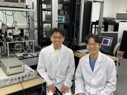
< Photo 1. Dr. Moojune Song (left) and Professor Kab-Jin Kim (right) of KAIST Department of Physics >
In simple terms, the researchers developed a special chip that synchronizes light and internal magnetic vibrations (magnons), enabling the transmission of phase information between distant magnets. They succeeded in observing and controlling interference between multiple signals in real time. This marks the first experimental evidence that magnets can serve as key components in quantum computing, serving as a pivotal step toward magnet-based quantum platforms.
The N and S poles of a magnet stem from the spin of electrons inside atoms. When many atoms align, their collective spin vibrations create a quantum particle known as a “magnon.”
Magnons are especially promising because of their nonreciprocal nature—they can carry information in only one direction, which makes them suitable for quantum noise isolation in compact quantum chips. They can also couple with both light and microwaves, enabling the potential for long-distance quantum communication over tens of kilometers.
Moreover, using special materials like antiferromagnets could allow quantum computers to operate at terahertz (THz) frequencies, far surpassing today’s hardware limitations, and possibly enabling room-temperature quantum computing without the need for bulky cryogenic equipment.
To build such a system, however, one must be able to transmit, measure, and control the phase information of magnons—the starting point and propagation of their waveforms—in real time. This had not been achieved until now.
< Figure 1. Superconducting Circuit-Based Magnon-Photon Hybrid System. (a) Schematic diagram of the device. A NbN superconducting resonator circuit fabricated on a silicon substrate is coupled with spherical YIG magnets (250 μm diameter), and magnons are generated and measured in real-time via a vertical antenna. (b) Photograph of the actual device. The distance between the two YIG spheres is 12 mm, a distance at which they cannot influence each other without the superconducting circuit. >
Professor Kim’s team used two tiny magnetic spheres made of Yttrium Iron Garnet (YIG) placed 12 mm apart with a superconducting resonator in between—similar to those used in quantum processors by Google and IBM. They input pulses into one magnet and successfully observed lossless transmission of magnon vibrations to the second magnet via the superconducting circuit.
They confirmed that from single nanosecond pulses to four microwave pulses, the magnon vibrations maintained their phase information and demonstrated predictable constructive or destructive interference in real time—known as coherent interference.
By adjusting the pulse frequencies and their intervals, the researchers could also freely control the interference patterns of magnons, effectively showing for the first time that electrical signals can be used to manipulate magnonic quantum states.
This work demonstrated that quantum gate operations using multiple pulses—a fundamental technique in quantum information processing—can be implemented using a hybrid system of magnetic materials and superconducting circuits. This opens the door for the practical use of magnet-based quantum devices.
< Figure 2. Experimental Data. (a) Measurement results of magnon-magnon band anticrossing via continuous wave measurement, showing the formation of a strong coupling hybrid system. (b) Magnon pulse exchange oscillation phenomenon between YIG spheres upon single pulse application. It can be seen that magnon information is coherently transmitted at regular time intervals through the superconducting circuit. (c,d) Magnon interference phenomenon upon dual pulse application. The magnon information state can be arbitrarily controlled by adjusting the time interval and carrier frequency between pulses. >
Professor Kab-Jin Kim stated, “This project began with a bold, even unconventional idea proposed to the Global Singularity Research Program: ‘What if we could build a quantum computer with magnets?’ The journey has been fascinating, and this study not only opens a new field of quantum spintronics, but also marks a turning point in developing high-efficiency quantum information processing devices.”
The research was co-led by postdoctoral researcher Moojune Song (KAIST), Dr. Yi Li and Dr. Valentine Novosad from Argonne National Lab, and Prof. Axel Hoffmann’s team at UIUC. The results were published in Nature Communications on April 17 and npj Spintronics on April 1, 2025.
Paper 1: Single-shot magnon interference in a magnon-superconducting-resonator hybrid circuit, Nat. Commun. 16, 3649 (2025)
DOI: https://doi.org/10.1038/s41467-025-58482-2
Paper 2: Single-shot electrical detection of short-wavelength magnon pulse transmission in a magnonic ultra-thin-film waveguide, npj Spintronics 3, 12 (2025)
DOI: https://doi.org/10.1038/s44306-025-00072-5
The research was supported by KAIST’s Global Singularity Research Initiative, the National Research Foundation of Korea (including the Mid-Career Researcher, Leading Research Center, and Quantum Information Science Human Resource Development programs), and the U.S. Department of Energy.
2025.06.12 View 2003
KAIST Turns an Unprecedented Idea into Reality: Quantum Computing with Magnets
What started as an idea under KAIST’s Global Singularity Research Project—"Can we build a quantum computer using magnets?"—has now become a scientific reality. A KAIST-led international research team has successfully demonstrated a core quantum computing technology using magnetic materials (ferromagnets) for the first time in the world.
KAIST (represented by President Kwang-Hyung Lee) announced on the 6th of May that a team led by Professor Kab-Jin Kim from the Department of Physics, in collaboration with the Argonne National Laboratory and the University of Illinois Urbana-Champaign (UIUC), has developed a “photon-magnon hybrid chip” and successfully implemented real-time, multi-pulse interference using magnetic materials—marking a global first.
< Photo 1. Dr. Moojune Song (left) and Professor Kab-Jin Kim (right) of KAIST Department of Physics >
In simple terms, the researchers developed a special chip that synchronizes light and internal magnetic vibrations (magnons), enabling the transmission of phase information between distant magnets. They succeeded in observing and controlling interference between multiple signals in real time. This marks the first experimental evidence that magnets can serve as key components in quantum computing, serving as a pivotal step toward magnet-based quantum platforms.
The N and S poles of a magnet stem from the spin of electrons inside atoms. When many atoms align, their collective spin vibrations create a quantum particle known as a “magnon.”
Magnons are especially promising because of their nonreciprocal nature—they can carry information in only one direction, which makes them suitable for quantum noise isolation in compact quantum chips. They can also couple with both light and microwaves, enabling the potential for long-distance quantum communication over tens of kilometers.
Moreover, using special materials like antiferromagnets could allow quantum computers to operate at terahertz (THz) frequencies, far surpassing today’s hardware limitations, and possibly enabling room-temperature quantum computing without the need for bulky cryogenic equipment.
To build such a system, however, one must be able to transmit, measure, and control the phase information of magnons—the starting point and propagation of their waveforms—in real time. This had not been achieved until now.
< Figure 1. Superconducting Circuit-Based Magnon-Photon Hybrid System. (a) Schematic diagram of the device. A NbN superconducting resonator circuit fabricated on a silicon substrate is coupled with spherical YIG magnets (250 μm diameter), and magnons are generated and measured in real-time via a vertical antenna. (b) Photograph of the actual device. The distance between the two YIG spheres is 12 mm, a distance at which they cannot influence each other without the superconducting circuit. >
Professor Kim’s team used two tiny magnetic spheres made of Yttrium Iron Garnet (YIG) placed 12 mm apart with a superconducting resonator in between—similar to those used in quantum processors by Google and IBM. They input pulses into one magnet and successfully observed lossless transmission of magnon vibrations to the second magnet via the superconducting circuit.
They confirmed that from single nanosecond pulses to four microwave pulses, the magnon vibrations maintained their phase information and demonstrated predictable constructive or destructive interference in real time—known as coherent interference.
By adjusting the pulse frequencies and their intervals, the researchers could also freely control the interference patterns of magnons, effectively showing for the first time that electrical signals can be used to manipulate magnonic quantum states.
This work demonstrated that quantum gate operations using multiple pulses—a fundamental technique in quantum information processing—can be implemented using a hybrid system of magnetic materials and superconducting circuits. This opens the door for the practical use of magnet-based quantum devices.
< Figure 2. Experimental Data. (a) Measurement results of magnon-magnon band anticrossing via continuous wave measurement, showing the formation of a strong coupling hybrid system. (b) Magnon pulse exchange oscillation phenomenon between YIG spheres upon single pulse application. It can be seen that magnon information is coherently transmitted at regular time intervals through the superconducting circuit. (c,d) Magnon interference phenomenon upon dual pulse application. The magnon information state can be arbitrarily controlled by adjusting the time interval and carrier frequency between pulses. >
Professor Kab-Jin Kim stated, “This project began with a bold, even unconventional idea proposed to the Global Singularity Research Program: ‘What if we could build a quantum computer with magnets?’ The journey has been fascinating, and this study not only opens a new field of quantum spintronics, but also marks a turning point in developing high-efficiency quantum information processing devices.”
The research was co-led by postdoctoral researcher Moojune Song (KAIST), Dr. Yi Li and Dr. Valentine Novosad from Argonne National Lab, and Prof. Axel Hoffmann’s team at UIUC. The results were published in Nature Communications on April 17 and npj Spintronics on April 1, 2025.
Paper 1: Single-shot magnon interference in a magnon-superconducting-resonator hybrid circuit, Nat. Commun. 16, 3649 (2025)
DOI: https://doi.org/10.1038/s41467-025-58482-2
Paper 2: Single-shot electrical detection of short-wavelength magnon pulse transmission in a magnonic ultra-thin-film waveguide, npj Spintronics 3, 12 (2025)
DOI: https://doi.org/10.1038/s44306-025-00072-5
The research was supported by KAIST’s Global Singularity Research Initiative, the National Research Foundation of Korea (including the Mid-Career Researcher, Leading Research Center, and Quantum Information Science Human Resource Development programs), and the U.S. Department of Energy.
2025.06.12 View 2003 -
 KAIST Develops Neuromorphic Semiconductor Chip that Learns and Corrects Itself
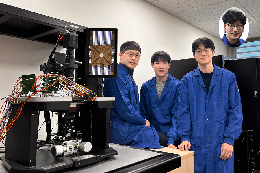
< Photo. The research team of the School of Electrical Engineering posed by the newly deveoped processor. (From center to the right) Professor Young-Gyu Yoon, Integrated Master's and Doctoral Program Students Seungjae Han and Hakcheon Jeong and Professor Shinhyun Choi >
- Professor Shinhyun Choi and Professor Young-Gyu Yoon’s Joint Research Team from the School of Electrical Engineering developed a computing chip that can learn, correct errors, and process AI tasks
- Equipping a computing chip with high-reliability memristor devices with self-error correction functions for real-time learning and image processing
Existing computer systems have separate data processing and storage devices, making them inefficient for processing complex data like AI. A KAIST research team has developed a memristor-based integrated system similar to the way our brain processes information. It is now ready for application in various devices including smart security cameras, allowing them to recognize suspicious activity immediately without having to rely on remote cloud servers, and medical devices with which it can help analyze health data in real time.
KAIST (President Kwang Hyung Lee) announced on the 17th of January that the joint research team of Professor Shinhyun Choi and Professor Young-Gyu Yoon of the School of Electrical Engineering has developed a next-generation neuromorphic semiconductor-based ultra-small computing chip that can learn and correct errors on its own.
< Figure 1. Scanning electron microscope (SEM) image of a computing chip equipped with a highly reliable selector-less 32×32 memristor crossbar array (left). Hardware system developed for real-time artificial intelligence implementation (right). >
What is special about this computing chip is that it can learn and correct errors that occur due to non-ideal characteristics that were difficult to solve in existing neuromorphic devices. For example, when processing a video stream, the chip learns to automatically separate a moving object from the background, and it becomes better at this task over time.
This self-learning ability has been proven by achieving accuracy comparable to ideal computer simulations in real-time image processing. The research team's main achievement is that it has completed a system that is both reliable and practical, beyond the development of brain-like components.
The research team has developed the world's first memristor-based integrated system that can adapt to immediate environmental changes, and has presented an innovative solution that overcomes the limitations of existing technology.
< Figure 2. Background and foreground separation results of an image containing non-ideal characteristics of memristor devices (left). Real-time image separation results through on-device learning using the memristor computing chip developed by our research team (right). >
At the heart of this innovation is a next-generation semiconductor device called a memristor*. The variable resistance characteristics of this device can replace the role of synapses in neural networks, and by utilizing it, data storage and computation can be performed simultaneously, just like our brain cells.
*Memristor: A compound word of memory and resistor, next-generation electrical device whose resistance value is determined by the amount and direction of charge that has flowed between the two terminals in the past.
The research team designed a highly reliable memristor that can precisely control resistance changes and developed an efficient system that excludes complex compensation processes through self-learning. This study is significant in that it experimentally verified the commercialization possibility of a next-generation neuromorphic semiconductor-based integrated system that supports real-time learning and inference.
This technology will revolutionize the way artificial intelligence is used in everyday devices, allowing AI tasks to be processed locally without relying on remote cloud servers, making them faster, more privacy-protected, and more energy-efficient.
“This system is like a smart workspace where everything is within arm’s reach instead of having to go back and forth between desks and file cabinets,” explained KAIST researchers Hakcheon Jeong and Seungjae Han, who led the development of this technology. “This is similar to the way our brain processes information, where everything is processed efficiently at once at one spot.”
The research was conducted with Hakcheon Jeong and Seungjae Han, the students of Integrated Master's and Doctoral Program at KAIST School of Electrical Engineering being the co-first authors, the results of which was published online in the international academic journal, Nature Electronics, on January 8, 2025.
*Paper title: Self-supervised video processing with self-calibration on an analogue computing platform based on a selector-less memristor array ( https://doi.org/10.1038/s41928-024-01318-6 )
This research was supported by the Next-Generation Intelligent Semiconductor Technology Development Project, Excellent New Researcher Project and PIM AI Semiconductor Core Technology Development Project of the National Research Foundation of Korea, and the Electronics and Telecommunications Research Institute Research and Development Support Project of the Institute of Information & communications Technology Planning & Evaluation.
2025.01.17 View 7409
KAIST Develops Neuromorphic Semiconductor Chip that Learns and Corrects Itself
< Photo. The research team of the School of Electrical Engineering posed by the newly deveoped processor. (From center to the right) Professor Young-Gyu Yoon, Integrated Master's and Doctoral Program Students Seungjae Han and Hakcheon Jeong and Professor Shinhyun Choi >
- Professor Shinhyun Choi and Professor Young-Gyu Yoon’s Joint Research Team from the School of Electrical Engineering developed a computing chip that can learn, correct errors, and process AI tasks
- Equipping a computing chip with high-reliability memristor devices with self-error correction functions for real-time learning and image processing
Existing computer systems have separate data processing and storage devices, making them inefficient for processing complex data like AI. A KAIST research team has developed a memristor-based integrated system similar to the way our brain processes information. It is now ready for application in various devices including smart security cameras, allowing them to recognize suspicious activity immediately without having to rely on remote cloud servers, and medical devices with which it can help analyze health data in real time.
KAIST (President Kwang Hyung Lee) announced on the 17th of January that the joint research team of Professor Shinhyun Choi and Professor Young-Gyu Yoon of the School of Electrical Engineering has developed a next-generation neuromorphic semiconductor-based ultra-small computing chip that can learn and correct errors on its own.
< Figure 1. Scanning electron microscope (SEM) image of a computing chip equipped with a highly reliable selector-less 32×32 memristor crossbar array (left). Hardware system developed for real-time artificial intelligence implementation (right). >
What is special about this computing chip is that it can learn and correct errors that occur due to non-ideal characteristics that were difficult to solve in existing neuromorphic devices. For example, when processing a video stream, the chip learns to automatically separate a moving object from the background, and it becomes better at this task over time.
This self-learning ability has been proven by achieving accuracy comparable to ideal computer simulations in real-time image processing. The research team's main achievement is that it has completed a system that is both reliable and practical, beyond the development of brain-like components.
The research team has developed the world's first memristor-based integrated system that can adapt to immediate environmental changes, and has presented an innovative solution that overcomes the limitations of existing technology.
< Figure 2. Background and foreground separation results of an image containing non-ideal characteristics of memristor devices (left). Real-time image separation results through on-device learning using the memristor computing chip developed by our research team (right). >
At the heart of this innovation is a next-generation semiconductor device called a memristor*. The variable resistance characteristics of this device can replace the role of synapses in neural networks, and by utilizing it, data storage and computation can be performed simultaneously, just like our brain cells.
*Memristor: A compound word of memory and resistor, next-generation electrical device whose resistance value is determined by the amount and direction of charge that has flowed between the two terminals in the past.
The research team designed a highly reliable memristor that can precisely control resistance changes and developed an efficient system that excludes complex compensation processes through self-learning. This study is significant in that it experimentally verified the commercialization possibility of a next-generation neuromorphic semiconductor-based integrated system that supports real-time learning and inference.
This technology will revolutionize the way artificial intelligence is used in everyday devices, allowing AI tasks to be processed locally without relying on remote cloud servers, making them faster, more privacy-protected, and more energy-efficient.
“This system is like a smart workspace where everything is within arm’s reach instead of having to go back and forth between desks and file cabinets,” explained KAIST researchers Hakcheon Jeong and Seungjae Han, who led the development of this technology. “This is similar to the way our brain processes information, where everything is processed efficiently at once at one spot.”
The research was conducted with Hakcheon Jeong and Seungjae Han, the students of Integrated Master's and Doctoral Program at KAIST School of Electrical Engineering being the co-first authors, the results of which was published online in the international academic journal, Nature Electronics, on January 8, 2025.
*Paper title: Self-supervised video processing with self-calibration on an analogue computing platform based on a selector-less memristor array ( https://doi.org/10.1038/s41928-024-01318-6 )
This research was supported by the Next-Generation Intelligent Semiconductor Technology Development Project, Excellent New Researcher Project and PIM AI Semiconductor Core Technology Development Project of the National Research Foundation of Korea, and the Electronics and Telecommunications Research Institute Research and Development Support Project of the Institute of Information & communications Technology Planning & Evaluation.
2025.01.17 View 7409 -
 The World’s First Hacking-preventing Cryptographic Semiconductor Chip
With the dramatic increase in the amount of information exchanged between components or devices in the 5G/6G era, such as for the Internet of Things (IoT) and autonomous driving, hacking attacks are becoming more sophisticated. Consequently, enhancing security functions is essential for safely transmitting data between and among devices.
On February 29th, a KAIST research team led by Professors Yang-gyu Choi and Seung-tak Ryu from the School of Electrical Engineering announced the successful development of the world's first security cryptographic semiconductor.
The team has developed the Cryptoristor, a cryptographic transistor based on FinFET technology, produced through a 100% silicon-compatible process, for the first time in the world. Cryptoristor is a random number generator (RNG) with unparalleled characteristics, featuring a unique structure comprising a single transistor and a distinctive mechanism.
In all security environments, including artificial intelligence, the most crucial element is the RNG. In the most commonly used security chip, the Advanced Encryption Standard (AES), the RNG is a core component, occupying approximately 75% of the total chip area and more than 85% of its energy consumption. Hence, there is an urgent need for the development of low-power/ultra-small RNGs suitable for mobile or IoT devices.
Existing RNGs come with limitations as they lack compatibility with silicon CMOS processes and circuit-based RNGs occupy a large surface area.
In contrast, the team’s newly developed Cryptoristor, a cryptographic semiconductor based on a single-component structure, consumes and occupies less than .001 of the power and area compared to the current chips being used. Utilizing the inherent randomness of FinFETs, fabricated on a Silicon-on-Insulator (SOI) substrate with an insulating layer formed beneath the silicon, the team developed an RNG that unpredictably produces zeroes and ones.
< Figure 1. Conceptual diagram of the security cryptographic transistor device. >
Generally speaking, preventing hackers from predicting the encrypted algorithms during data exchanges through mobile devices is pivotal. Therefore, this method ensures unpredictability by generating random sequences of zeroes and ones that change every time.
Moreover, while the Cryptoristor-based RNG research is the world's first of its kind without any international implementation cases, it shares the same transistor structure as existing logic or memory components. This enables 100% production through rapid mass production processes using existing semiconductor facilities at a low cost.
Seung-il Kim, a PhD student who led the research, explained the significance of the study, stating, "As a cryptographic semiconductor, the ultra-small/low-power random number generator enhances security through its distinctive unpredictability, supporting safe hyperconnectivity with secure transmissions between chips or devices. Particularly, compared to previous research, it offers excellent advantages in terms of energy consumption, integration density, and cost, making it suitable for IoT device environments."
This research, with master’s student Hyung-jin Yoo as the co-author, was officially published in the online edition of Science Advances, a sister journal of Science, in February 2024 (research paper title: Cryptographic transistor for true random number generator with low power consumption).
This research received support from the Next-Generation Intelligent Semiconductor Technology Development Project and the Core Technology Development Project for the National Semiconductor Research Laboratory.
2024.03.07 View 8822
The World’s First Hacking-preventing Cryptographic Semiconductor Chip
With the dramatic increase in the amount of information exchanged between components or devices in the 5G/6G era, such as for the Internet of Things (IoT) and autonomous driving, hacking attacks are becoming more sophisticated. Consequently, enhancing security functions is essential for safely transmitting data between and among devices.
On February 29th, a KAIST research team led by Professors Yang-gyu Choi and Seung-tak Ryu from the School of Electrical Engineering announced the successful development of the world's first security cryptographic semiconductor.
The team has developed the Cryptoristor, a cryptographic transistor based on FinFET technology, produced through a 100% silicon-compatible process, for the first time in the world. Cryptoristor is a random number generator (RNG) with unparalleled characteristics, featuring a unique structure comprising a single transistor and a distinctive mechanism.
In all security environments, including artificial intelligence, the most crucial element is the RNG. In the most commonly used security chip, the Advanced Encryption Standard (AES), the RNG is a core component, occupying approximately 75% of the total chip area and more than 85% of its energy consumption. Hence, there is an urgent need for the development of low-power/ultra-small RNGs suitable for mobile or IoT devices.
Existing RNGs come with limitations as they lack compatibility with silicon CMOS processes and circuit-based RNGs occupy a large surface area.
In contrast, the team’s newly developed Cryptoristor, a cryptographic semiconductor based on a single-component structure, consumes and occupies less than .001 of the power and area compared to the current chips being used. Utilizing the inherent randomness of FinFETs, fabricated on a Silicon-on-Insulator (SOI) substrate with an insulating layer formed beneath the silicon, the team developed an RNG that unpredictably produces zeroes and ones.
< Figure 1. Conceptual diagram of the security cryptographic transistor device. >
Generally speaking, preventing hackers from predicting the encrypted algorithms during data exchanges through mobile devices is pivotal. Therefore, this method ensures unpredictability by generating random sequences of zeroes and ones that change every time.
Moreover, while the Cryptoristor-based RNG research is the world's first of its kind without any international implementation cases, it shares the same transistor structure as existing logic or memory components. This enables 100% production through rapid mass production processes using existing semiconductor facilities at a low cost.
Seung-il Kim, a PhD student who led the research, explained the significance of the study, stating, "As a cryptographic semiconductor, the ultra-small/low-power random number generator enhances security through its distinctive unpredictability, supporting safe hyperconnectivity with secure transmissions between chips or devices. Particularly, compared to previous research, it offers excellent advantages in terms of energy consumption, integration density, and cost, making it suitable for IoT device environments."
This research, with master’s student Hyung-jin Yoo as the co-author, was officially published in the online edition of Science Advances, a sister journal of Science, in February 2024 (research paper title: Cryptographic transistor for true random number generator with low power consumption).
This research received support from the Next-Generation Intelligent Semiconductor Technology Development Project and the Core Technology Development Project for the National Semiconductor Research Laboratory.
2024.03.07 View 8822 -
 A KAIST research team develops a high-performance modular SSD system semiconductor
In recent years, there has been a rise in demand for large amounts of data to train AI models and, thus, data size has become increasingly important over time. Accordingly, solid state drives (SSDs, storage devices that use a semiconductor memory unit), which are core storage devices for data centers and cloud services, have also seen an increase in demand. However, the internal components of higher performing SSDs have become more tightly coupled, and this tightly-coupled structure limits SSD from maximized performance.
On June 15, a KAIST research team led by Professor Dongjun Kim (John Kim) from the School of Electrical Engineering (EE) announced the development of the first SSD system semiconductor structure that can increase the reading/writing performance of next generation SSDs and extend their lifespan through high-performance modular SSD systems.
Professor Kim’s team identified the limitations of the tightly-coupled structures in existing SSD designs and proposed a de-coupled structure that can maximize SSD performance by configuring an internal on-chip network specialized for flash memory. This technique utilizes on-chip network technology, which can freely send packet-based data within the chip and is often used to design non-memory system semiconductors like CPUs and GPUs. Through this, the team developed a ‘modular SSD’, which shows reduced interdependence between front-end and back-end designs, and allows their independent design and assembly.
*on-chip network: a packet-based connection structure for the internal components of system semiconductors like CPUs/GPUs. On-chip networks are one of the most critical design components for high-performing system semiconductors, and their importance grows with the size of the semiconductor chip.
Professor Kim’s team refers to the components nearer to the CPU as the front-end and the parts closer to the flash memory as back-end. They newly constructed an on-chip network specific to flash memory in order to allow data transmission between the back-end’s flash controller, proposing a de-coupled structure that can minimize performance drop.
The SSD can accelerate some functions of the flash translation layer, a critical element to drive the SSD, in order to allow flash memory to actively overcome its limitations. Another advantage of the de-coupled, modular structure is that the flash translation layer is not limited to the characteristics of specific flash memories. Instead, their front-end and back-end designs can be carried out independently. Through this, the team could produce 21-times faster response times compared to existing systems and extend SSD lifespan by 23% by also applying the DDS defect detection technique.
< Figure 1. Schematic diagram of the structure of a high-performance modular SSD system developed by Professor Dong-Jun Kim's team >
This research, conducted by first author and Ph.D. candidate Jiho Kim from the KAIST School of EE and co-author Professor Myoungsoo Jung, was presented on the 19th of June at the 50th IEEE/ACM International Symposium on Computer Architecture, the most prestigious academic conference in the field of computer architecture, held in Orlando, Florida. (Paper Title: Decoupled SSD: Rethinking SSD Architecture through Network-based Flash Controllers)
< Figure 2. Conceptual diagram of hardware acceleration through high-performance modular SSD system >
Professor Dongjun Kim, who led the research, said, “This research is significant in that it identified the structural limitations of existing SSDs, and showed that on-chip network technology based on system memory semiconductors like CPUs can drive the hardware to actively carry out the necessary actions. We expect this to contribute greatly to the next-generation high-performance SSD market.” He added, “The de-coupled architecture is a structure that can actively operate to extend devices’ lifespan. In other words, its significance is not limited to the level of performance and can, therefore, be used for various applications.”
KAIST commented that this research is also meaningful in that the results were reaped through a collaborative study between two world-renowned researchers: Professor Myeongsoo Jung, recognized in the field of computer system storage devices, and Professor Dongjun Kim, a leading researcher in computer architecture and interconnection networks.
This research was funded by the National Research Foundation of Korea, Samsung Electronics, the IC Design Education Center, and Next Generation Semiconductor Technology and Development granted by the Institute of Information & Communications Technology, Planning & Evaluation.
2023.06.23 View 8127
A KAIST research team develops a high-performance modular SSD system semiconductor
In recent years, there has been a rise in demand for large amounts of data to train AI models and, thus, data size has become increasingly important over time. Accordingly, solid state drives (SSDs, storage devices that use a semiconductor memory unit), which are core storage devices for data centers and cloud services, have also seen an increase in demand. However, the internal components of higher performing SSDs have become more tightly coupled, and this tightly-coupled structure limits SSD from maximized performance.
On June 15, a KAIST research team led by Professor Dongjun Kim (John Kim) from the School of Electrical Engineering (EE) announced the development of the first SSD system semiconductor structure that can increase the reading/writing performance of next generation SSDs and extend their lifespan through high-performance modular SSD systems.
Professor Kim’s team identified the limitations of the tightly-coupled structures in existing SSD designs and proposed a de-coupled structure that can maximize SSD performance by configuring an internal on-chip network specialized for flash memory. This technique utilizes on-chip network technology, which can freely send packet-based data within the chip and is often used to design non-memory system semiconductors like CPUs and GPUs. Through this, the team developed a ‘modular SSD’, which shows reduced interdependence between front-end and back-end designs, and allows their independent design and assembly.
*on-chip network: a packet-based connection structure for the internal components of system semiconductors like CPUs/GPUs. On-chip networks are one of the most critical design components for high-performing system semiconductors, and their importance grows with the size of the semiconductor chip.
Professor Kim’s team refers to the components nearer to the CPU as the front-end and the parts closer to the flash memory as back-end. They newly constructed an on-chip network specific to flash memory in order to allow data transmission between the back-end’s flash controller, proposing a de-coupled structure that can minimize performance drop.
The SSD can accelerate some functions of the flash translation layer, a critical element to drive the SSD, in order to allow flash memory to actively overcome its limitations. Another advantage of the de-coupled, modular structure is that the flash translation layer is not limited to the characteristics of specific flash memories. Instead, their front-end and back-end designs can be carried out independently. Through this, the team could produce 21-times faster response times compared to existing systems and extend SSD lifespan by 23% by also applying the DDS defect detection technique.
< Figure 1. Schematic diagram of the structure of a high-performance modular SSD system developed by Professor Dong-Jun Kim's team >
This research, conducted by first author and Ph.D. candidate Jiho Kim from the KAIST School of EE and co-author Professor Myoungsoo Jung, was presented on the 19th of June at the 50th IEEE/ACM International Symposium on Computer Architecture, the most prestigious academic conference in the field of computer architecture, held in Orlando, Florida. (Paper Title: Decoupled SSD: Rethinking SSD Architecture through Network-based Flash Controllers)
< Figure 2. Conceptual diagram of hardware acceleration through high-performance modular SSD system >
Professor Dongjun Kim, who led the research, said, “This research is significant in that it identified the structural limitations of existing SSDs, and showed that on-chip network technology based on system memory semiconductors like CPUs can drive the hardware to actively carry out the necessary actions. We expect this to contribute greatly to the next-generation high-performance SSD market.” He added, “The de-coupled architecture is a structure that can actively operate to extend devices’ lifespan. In other words, its significance is not limited to the level of performance and can, therefore, be used for various applications.”
KAIST commented that this research is also meaningful in that the results were reaped through a collaborative study between two world-renowned researchers: Professor Myeongsoo Jung, recognized in the field of computer system storage devices, and Professor Dongjun Kim, a leading researcher in computer architecture and interconnection networks.
This research was funded by the National Research Foundation of Korea, Samsung Electronics, the IC Design Education Center, and Next Generation Semiconductor Technology and Development granted by the Institute of Information & Communications Technology, Planning & Evaluation.
2023.06.23 View 8127 -
 KAIST develops 'MetaVRain' that realizes vivid 3D real-life images
KAIST (President Kwang Hyung Lee) is a high-speed, low-power artificial intelligence (AI: Artificial Intelligent) semiconductor* MetaVRain, which implements artificial intelligence-based 3D rendering that can render images close to real life on mobile devices.
* AI semiconductor: Semiconductor equipped with artificial intelligence processing functions such as recognition, reasoning, learning, and judgment, and implemented with optimized technology based on super intelligence, ultra-low power, and ultra-reliability
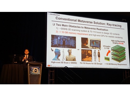
The artificial intelligence semiconductor developed by the research team makes the existing ray-tracing*-based 3D rendering driven by GPU into artificial intelligence-based 3D rendering on a newly manufactured AI semiconductor, making it a 3D video capture studio that requires enormous costs. is not needed, so the cost of 3D model production can be greatly reduced and the memory used can be reduced by more than 180 times. In particular, the existing 3D graphic editing and design, which used complex software such as Blender, is replaced with simple artificial intelligence learning, so the general public can easily apply and edit the desired style.
* Ray-tracing: Technology that obtains images close to real life by tracing the trajectory of all light rays that change according to the light source, shape and texture of the object
This research, in which doctoral student Donghyun Han participated as the first author, was presented at the International Solid-State Circuit Design Conference (ISSCC) held in San Francisco, USA from February 18th to 22nd by semiconductor researchers from all over the world.
(Paper Number 2.7, Paper Title: MetaVRain: A 133mW Real-time Hyper-realistic 3D NeRF Processor with 1D-2D Hybrid Neural Engines for Metaverse on Mobile Devices (Authors: Donghyeon Han, Junha Ryu, Sangyeob Kim, Sangjin Kim, and Hoi-Jun Yoo))
Professor Yoo's team discovered inefficient operations that occur when implementing 3D rendering through artificial intelligence, and developed a new concept semiconductor that combines human visual recognition methods to reduce them. When a person remembers an object, he has the cognitive ability to immediately guess what the current object looks like based on the process of starting with a rough outline and gradually specifying its shape, and if it is an object he saw right before. In imitation of such a human cognitive process, the newly developed semiconductor adopts an operation method that grasps the rough shape of an object in advance through low-resolution voxels and minimizes the amount of computation required for current rendering based on the result of rendering in the past.
MetaVRain, developed by Professor Yu's team, achieved the world's best performance by developing a state-of-the-art CMOS chip as well as a hardware architecture that mimics the human visual recognition process. MetaVRain is optimized for artificial intelligence-based 3D rendering technology and achieves a rendering speed of up to 100 FPS or more, which is 911 times faster than conventional GPUs. In addition, as a result of the study, the energy efficiency, which represents the energy consumed per video screen processing, is 26,400 times higher than that of GPU, opening the possibility of artificial intelligence-based real-time rendering in VR/AR headsets and mobile devices.
To show an example of using MetaVRain, the research team developed a smart 3D rendering application system together, and showed an example of changing the style of a 3D model according to the user's preferred style. Since you only need to give artificial intelligence an image of the desired style and perform re-learning, you can easily change the style of the 3D model without the help of complicated software. In addition to the example of the application system implemented by Professor Yu's team, it is expected that various application examples will be possible, such as creating a realistic 3D avatar modeled after a user's face, creating 3D models of various structures, and changing the weather according to the film production environment. do.
Starting with MetaVRain, the research team expects that the field of 3D graphics will also begin to be replaced by artificial intelligence, and revealed that the combination of artificial intelligence and 3D graphics is a great technological innovation for the realization of the metaverse.
Professor Hoi-Jun Yoo of the Department of Electrical and Electronic Engineering at KAIST, who led the research, said, “Currently, 3D graphics are focused on depicting what an object looks like, not how people see it.” The significance of this study was revealed as a study that enabled efficient 3D graphics by borrowing the way people recognize and express objects by imitating them.” He also foresaw the future, saying, “The realization of the metaverse will be achieved through innovation in artificial intelligence technology and innovation in artificial intelligence semiconductors, as shown in this study.”
Figure 1. Description of the MetaVRain demo screen
Photo of Presentation at the International Solid-State Circuits Conference (ISSCC)
2023.03.13 View 8283
KAIST develops 'MetaVRain' that realizes vivid 3D real-life images
KAIST (President Kwang Hyung Lee) is a high-speed, low-power artificial intelligence (AI: Artificial Intelligent) semiconductor* MetaVRain, which implements artificial intelligence-based 3D rendering that can render images close to real life on mobile devices.
* AI semiconductor: Semiconductor equipped with artificial intelligence processing functions such as recognition, reasoning, learning, and judgment, and implemented with optimized technology based on super intelligence, ultra-low power, and ultra-reliability
The artificial intelligence semiconductor developed by the research team makes the existing ray-tracing*-based 3D rendering driven by GPU into artificial intelligence-based 3D rendering on a newly manufactured AI semiconductor, making it a 3D video capture studio that requires enormous costs. is not needed, so the cost of 3D model production can be greatly reduced and the memory used can be reduced by more than 180 times. In particular, the existing 3D graphic editing and design, which used complex software such as Blender, is replaced with simple artificial intelligence learning, so the general public can easily apply and edit the desired style.
* Ray-tracing: Technology that obtains images close to real life by tracing the trajectory of all light rays that change according to the light source, shape and texture of the object
This research, in which doctoral student Donghyun Han participated as the first author, was presented at the International Solid-State Circuit Design Conference (ISSCC) held in San Francisco, USA from February 18th to 22nd by semiconductor researchers from all over the world.
(Paper Number 2.7, Paper Title: MetaVRain: A 133mW Real-time Hyper-realistic 3D NeRF Processor with 1D-2D Hybrid Neural Engines for Metaverse on Mobile Devices (Authors: Donghyeon Han, Junha Ryu, Sangyeob Kim, Sangjin Kim, and Hoi-Jun Yoo))
Professor Yoo's team discovered inefficient operations that occur when implementing 3D rendering through artificial intelligence, and developed a new concept semiconductor that combines human visual recognition methods to reduce them. When a person remembers an object, he has the cognitive ability to immediately guess what the current object looks like based on the process of starting with a rough outline and gradually specifying its shape, and if it is an object he saw right before. In imitation of such a human cognitive process, the newly developed semiconductor adopts an operation method that grasps the rough shape of an object in advance through low-resolution voxels and minimizes the amount of computation required for current rendering based on the result of rendering in the past.
MetaVRain, developed by Professor Yu's team, achieved the world's best performance by developing a state-of-the-art CMOS chip as well as a hardware architecture that mimics the human visual recognition process. MetaVRain is optimized for artificial intelligence-based 3D rendering technology and achieves a rendering speed of up to 100 FPS or more, which is 911 times faster than conventional GPUs. In addition, as a result of the study, the energy efficiency, which represents the energy consumed per video screen processing, is 26,400 times higher than that of GPU, opening the possibility of artificial intelligence-based real-time rendering in VR/AR headsets and mobile devices.
To show an example of using MetaVRain, the research team developed a smart 3D rendering application system together, and showed an example of changing the style of a 3D model according to the user's preferred style. Since you only need to give artificial intelligence an image of the desired style and perform re-learning, you can easily change the style of the 3D model without the help of complicated software. In addition to the example of the application system implemented by Professor Yu's team, it is expected that various application examples will be possible, such as creating a realistic 3D avatar modeled after a user's face, creating 3D models of various structures, and changing the weather according to the film production environment. do.
Starting with MetaVRain, the research team expects that the field of 3D graphics will also begin to be replaced by artificial intelligence, and revealed that the combination of artificial intelligence and 3D graphics is a great technological innovation for the realization of the metaverse.
Professor Hoi-Jun Yoo of the Department of Electrical and Electronic Engineering at KAIST, who led the research, said, “Currently, 3D graphics are focused on depicting what an object looks like, not how people see it.” The significance of this study was revealed as a study that enabled efficient 3D graphics by borrowing the way people recognize and express objects by imitating them.” He also foresaw the future, saying, “The realization of the metaverse will be achieved through innovation in artificial intelligence technology and innovation in artificial intelligence semiconductors, as shown in this study.”
Figure 1. Description of the MetaVRain demo screen
Photo of Presentation at the International Solid-State Circuits Conference (ISSCC)
2023.03.13 View 8283 -
 Shaping the AI Semiconductor Ecosystem
- As the marriage of AI and semiconductor being highlighted as the strategic technology of national enthusiasm, KAIST's achievements in the related fields accumulated through top-class education and research capabilities that surpass that of peer universities around the world are standing far apart from the rest of the pack.
As Artificial Intelligence Semiconductor, or a system of semiconductors designed for specifically for highly complicated computation need for AI to conduct its learning and deducing calculations, (hereafter AI semiconductors) stand out as a national strategic technology, the related achievements of KAIST, headed by President Kwang Hyung Lee, are also attracting attention. The Ministry of Science, ICT and Future Planning (MSIT) of Korea initiated a program to support the advancement of AI semiconductor last year with the goal of occupying 20% of the global AI semiconductor market by 2030. This year, through industry-university-research discussions, the Ministry expanded to the program with the addition of 1.2 trillion won of investment over five years through 'Support Plan for AI Semiconductor Industry Promotion'. Accordingly, major universities began putting together programs devised to train students to develop expertise in AI semiconductors.
KAIST has accumulated top-notch educational and research capabilities in the two core fields of AI semiconductor - Semiconductor and Artificial Intelligence. Notably, in the field of semiconductors, the International Solid-State Circuit Conference (ISSCC) is the world's most prestigious conference about designing of semiconductor integrated circuit. Established in 1954, with more than 60% of the participants coming from companies including Samsung, Qualcomm, TSMC, and Intel, the conference naturally focuses on practical value of the studies from the industrial point-of-view, earning the nickname the ‘Semiconductor Design Olympics’. At such conference of legacy and influence, KAIST kept its presence widely visible over other participating universities, leading in terms of the number of accepted papers over world-class schools such as Massachusetts Institute of Technology (MIT) and Stanford for the past 17 years.
Number of papers published at the InternationalSolid-State Circuit Conference (ISSCC) in 2022 sorted by nations and by institutions
Number of papers by universities presented at the International Solid-State Circuit Conference (ISCCC) in 2006~2022
In terms of the number of papers accepted at the ISSCC, KAIST ranked among top two universities each year since 2006. Looking at the average number of accepted papers over the past 17 years, KAIST stands out as an unparalleled leader. The average number of KAIST papers adopted during the period of 17 years from 2006 through 2022, was 8.4, which is almost double of that of competitors like MIT (4.6) and UCLA (3.6). In Korea, it maintains the second place overall after Samsung, the undisputed number one in the semiconductor design field. Also, this year, KAIST was ranked first among universities participating at the Symposium on VLSI Technology and Circuits, an academic conference in the field of integrated circuits that rivals the ISSCC.
Number of papers adopted by the Symposium on VLSI Technology and Circuits in 2022 submitted from the universities
With KAIST researchers working and presenting new technologies at the frontiers of all key areas of the semiconductor industry, the quality of KAIST research is also maintained at the highest level. Professor Myoungsoo Jung's research team in the School of Electrical Engineering is actively working to develop heterogeneous computing environment with high energy efficiency in response to the industry's demand for high performance at low power. In the field of materials, a research team led by Professor Byong-Guk Park of the Department of Materials Science and Engineering developed the Spin Orbit Torque (SOT)-based Magnetic RAM (MRAM) memory that operates at least 10 times faster than conventional memories to suggest a way to overcome the limitations of the existing 'von Neumann structure'.
As such, while providing solutions to major challenges in the current semiconductor industry, the development of new technologies necessary to preoccupy new fields in the semiconductor industry are also very actively pursued. In the field of Quantum Computing, which is attracting attention as next-generation computing technology needed in order to take the lead in the fields of cryptography and nonlinear computation, Professor Sanghyeon Kim's research team in the School of Electrical Engineering presented the world's first 3D integrated quantum computing system at 2021 VLSI Symposium. In Neuromorphic Computing, which is expected to bring remarkable advancements in the field of artificial intelligence by utilizing the principles of the neurology, the research team of Professor Shinhyun Choi of School of Electrical Engineering is developing a next-generation memristor that mimics neurons.
The number of papers by the International Conference on Machine Learning (ICML) and the Conference on Neural Information Processing Systems (NeurIPS), two of the world’s most prestigious academic societies in the field of artificial intelligence (KAIST 6th in the world, 1st in Asia, in 2020)
The field of artificial intelligence has also grown rapidly. Based on the number of papers from the International Conference on Machine Learning (ICML) and the Conference on Neural Information Processing Systems (NeurIPS), two of the world's most prestigious conferences in the field of artificial intelligence, KAIST ranked 6th in the world in 2020 and 1st in Asia. Since 2012, KAIST's ranking steadily inclined from 37th to 6th, climbing 31 steps over the period of eight years. In 2021, 129 papers, or about 40%, of Korean papers published at 11 top artificial intelligence conferences were presented by KAIST. Thanks to KAIST's efforts, in 2021, Korea ranked sixth after the United States, China, United Kingdom, Canada, and Germany in terms of the number of papers published by global AI academic societies.
Number of papers from Korea (and by KAIST) published at 11 top conferences in the field of artificial intelligence in 2021
In terms of content, KAIST's AI research is also at the forefront. Professor Hoi-Jun Yoo's research team in the School of Electrical Engineering compensated for the shortcomings of the “edge networks” by implementing artificial intelligence real-time learning networks on mobile devices. In order to materialize artificial intelligence, data accumulation and a huge amount of computation is required. For this, a high-performance server takes care of massive computation, and for the user terminals, the “edge network” that collects data and performs simple computations are used. Professor Yoo's research greatly increased AI’s processing speed and performance by allotting the learning task to the user terminal as well.
In June, a research team led by Professor Min-Soo Kim of the School of Computing presented a solution that is essential for processing super-scale artificial intelligence models. The super-scale machine learning system developed by the research team is expected to achieve speeds up to 8.8 times faster than Google's Tensorflow or IBM's System DS, which are mainly used in the industry.
KAIST is also making remarkable achievements in the field of AI semiconductors. In 2020, Professor Minsoo Rhu's research team in the School of Electrical Engineering succeeded in developing the world's first AI semiconductor optimized for AI recommendation systems. Due to the nature of the AI recommendation system having to handle vast amounts of contents and user information, it quickly meets its limitation because of the information bottleneck when the process is operated through a general-purpose artificial intelligence system. Professor Minsoo Rhu's team developed a semiconductor that can achieve a speed that is 21 times faster than existing systems using the 'Processing-In-Memory (PIM)' technology. PIM is a technology that improves efficiency by performing the calculations in 'RAM', or random-access memory, which is usually only used to store data temporarily just before they are processed. When PIM technology is put out on the market, it is expected that fortify competitiveness of Korean companies in the AI semiconductor market drastically, as they already hold great strength in the memory area.
KAIST does not plan to be complacent with its achievements, but is making various plans to further the distance from the competitors catching on in the fields of artificial intelligence, semiconductors, and AI semiconductors. Following the establishment of the first artificial intelligence research center in Korea in 1990, the Kim Jaechul AI Graduate School was opened in 2019 to sustain the supply chain of the experts in the field. In 2020, Artificial Intelligence Semiconductor System Research Center was launched to conduct convergent research on AI and semiconductors, which was followed by the establishment of the AI Institutes to promote “AI+X” research efforts.
Based on the internal capabilities accumulated through these efforts, KAIST is also making efforts to train human resources needed in these areas. KAIST established joint research centers with companies such as Naver, while collaborating with local governments such as Hwaseong City to simultaneously nurture professional manpower. Back in 2021, KAIST signed an agreement to establish the Semiconductor System Engineering Department with Samsung Electronics and are preparing a new semiconductor specialist training program. The newly established Department of Semiconductor System Engineering will select around 100 new students every year from 2023 and provide special scholarships to all students so that they can develop their professional skills. In addition, through close cooperation with the industry, they will receive special support which includes field trips and internships at Samsung Electronics, and joint workshops and on-site training.
KAIST has made a significant contribution to the growth of the Korean semiconductor industry ecosystem, producing 25% of doctoral workers in the domestic semiconductor field and 20% of CEOs of mid-sized and venture companies with doctoral degrees. With the dawn coming up on the AI semiconductor ecosystem, whether KAIST will reprise the pivotal role seems to be the crucial point of business.
2022.08.05 View 13448
Shaping the AI Semiconductor Ecosystem
- As the marriage of AI and semiconductor being highlighted as the strategic technology of national enthusiasm, KAIST's achievements in the related fields accumulated through top-class education and research capabilities that surpass that of peer universities around the world are standing far apart from the rest of the pack.
As Artificial Intelligence Semiconductor, or a system of semiconductors designed for specifically for highly complicated computation need for AI to conduct its learning and deducing calculations, (hereafter AI semiconductors) stand out as a national strategic technology, the related achievements of KAIST, headed by President Kwang Hyung Lee, are also attracting attention. The Ministry of Science, ICT and Future Planning (MSIT) of Korea initiated a program to support the advancement of AI semiconductor last year with the goal of occupying 20% of the global AI semiconductor market by 2030. This year, through industry-university-research discussions, the Ministry expanded to the program with the addition of 1.2 trillion won of investment over five years through 'Support Plan for AI Semiconductor Industry Promotion'. Accordingly, major universities began putting together programs devised to train students to develop expertise in AI semiconductors.
KAIST has accumulated top-notch educational and research capabilities in the two core fields of AI semiconductor - Semiconductor and Artificial Intelligence. Notably, in the field of semiconductors, the International Solid-State Circuit Conference (ISSCC) is the world's most prestigious conference about designing of semiconductor integrated circuit. Established in 1954, with more than 60% of the participants coming from companies including Samsung, Qualcomm, TSMC, and Intel, the conference naturally focuses on practical value of the studies from the industrial point-of-view, earning the nickname the ‘Semiconductor Design Olympics’. At such conference of legacy and influence, KAIST kept its presence widely visible over other participating universities, leading in terms of the number of accepted papers over world-class schools such as Massachusetts Institute of Technology (MIT) and Stanford for the past 17 years.
Number of papers published at the InternationalSolid-State Circuit Conference (ISSCC) in 2022 sorted by nations and by institutions
Number of papers by universities presented at the International Solid-State Circuit Conference (ISCCC) in 2006~2022
In terms of the number of papers accepted at the ISSCC, KAIST ranked among top two universities each year since 2006. Looking at the average number of accepted papers over the past 17 years, KAIST stands out as an unparalleled leader. The average number of KAIST papers adopted during the period of 17 years from 2006 through 2022, was 8.4, which is almost double of that of competitors like MIT (4.6) and UCLA (3.6). In Korea, it maintains the second place overall after Samsung, the undisputed number one in the semiconductor design field. Also, this year, KAIST was ranked first among universities participating at the Symposium on VLSI Technology and Circuits, an academic conference in the field of integrated circuits that rivals the ISSCC.
Number of papers adopted by the Symposium on VLSI Technology and Circuits in 2022 submitted from the universities
With KAIST researchers working and presenting new technologies at the frontiers of all key areas of the semiconductor industry, the quality of KAIST research is also maintained at the highest level. Professor Myoungsoo Jung's research team in the School of Electrical Engineering is actively working to develop heterogeneous computing environment with high energy efficiency in response to the industry's demand for high performance at low power. In the field of materials, a research team led by Professor Byong-Guk Park of the Department of Materials Science and Engineering developed the Spin Orbit Torque (SOT)-based Magnetic RAM (MRAM) memory that operates at least 10 times faster than conventional memories to suggest a way to overcome the limitations of the existing 'von Neumann structure'.
As such, while providing solutions to major challenges in the current semiconductor industry, the development of new technologies necessary to preoccupy new fields in the semiconductor industry are also very actively pursued. In the field of Quantum Computing, which is attracting attention as next-generation computing technology needed in order to take the lead in the fields of cryptography and nonlinear computation, Professor Sanghyeon Kim's research team in the School of Electrical Engineering presented the world's first 3D integrated quantum computing system at 2021 VLSI Symposium. In Neuromorphic Computing, which is expected to bring remarkable advancements in the field of artificial intelligence by utilizing the principles of the neurology, the research team of Professor Shinhyun Choi of School of Electrical Engineering is developing a next-generation memristor that mimics neurons.
The number of papers by the International Conference on Machine Learning (ICML) and the Conference on Neural Information Processing Systems (NeurIPS), two of the world’s most prestigious academic societies in the field of artificial intelligence (KAIST 6th in the world, 1st in Asia, in 2020)
The field of artificial intelligence has also grown rapidly. Based on the number of papers from the International Conference on Machine Learning (ICML) and the Conference on Neural Information Processing Systems (NeurIPS), two of the world's most prestigious conferences in the field of artificial intelligence, KAIST ranked 6th in the world in 2020 and 1st in Asia. Since 2012, KAIST's ranking steadily inclined from 37th to 6th, climbing 31 steps over the period of eight years. In 2021, 129 papers, or about 40%, of Korean papers published at 11 top artificial intelligence conferences were presented by KAIST. Thanks to KAIST's efforts, in 2021, Korea ranked sixth after the United States, China, United Kingdom, Canada, and Germany in terms of the number of papers published by global AI academic societies.
Number of papers from Korea (and by KAIST) published at 11 top conferences in the field of artificial intelligence in 2021
In terms of content, KAIST's AI research is also at the forefront. Professor Hoi-Jun Yoo's research team in the School of Electrical Engineering compensated for the shortcomings of the “edge networks” by implementing artificial intelligence real-time learning networks on mobile devices. In order to materialize artificial intelligence, data accumulation and a huge amount of computation is required. For this, a high-performance server takes care of massive computation, and for the user terminals, the “edge network” that collects data and performs simple computations are used. Professor Yoo's research greatly increased AI’s processing speed and performance by allotting the learning task to the user terminal as well.
In June, a research team led by Professor Min-Soo Kim of the School of Computing presented a solution that is essential for processing super-scale artificial intelligence models. The super-scale machine learning system developed by the research team is expected to achieve speeds up to 8.8 times faster than Google's Tensorflow or IBM's System DS, which are mainly used in the industry.
KAIST is also making remarkable achievements in the field of AI semiconductors. In 2020, Professor Minsoo Rhu's research team in the School of Electrical Engineering succeeded in developing the world's first AI semiconductor optimized for AI recommendation systems. Due to the nature of the AI recommendation system having to handle vast amounts of contents and user information, it quickly meets its limitation because of the information bottleneck when the process is operated through a general-purpose artificial intelligence system. Professor Minsoo Rhu's team developed a semiconductor that can achieve a speed that is 21 times faster than existing systems using the 'Processing-In-Memory (PIM)' technology. PIM is a technology that improves efficiency by performing the calculations in 'RAM', or random-access memory, which is usually only used to store data temporarily just before they are processed. When PIM technology is put out on the market, it is expected that fortify competitiveness of Korean companies in the AI semiconductor market drastically, as they already hold great strength in the memory area.
KAIST does not plan to be complacent with its achievements, but is making various plans to further the distance from the competitors catching on in the fields of artificial intelligence, semiconductors, and AI semiconductors. Following the establishment of the first artificial intelligence research center in Korea in 1990, the Kim Jaechul AI Graduate School was opened in 2019 to sustain the supply chain of the experts in the field. In 2020, Artificial Intelligence Semiconductor System Research Center was launched to conduct convergent research on AI and semiconductors, which was followed by the establishment of the AI Institutes to promote “AI+X” research efforts.
Based on the internal capabilities accumulated through these efforts, KAIST is also making efforts to train human resources needed in these areas. KAIST established joint research centers with companies such as Naver, while collaborating with local governments such as Hwaseong City to simultaneously nurture professional manpower. Back in 2021, KAIST signed an agreement to establish the Semiconductor System Engineering Department with Samsung Electronics and are preparing a new semiconductor specialist training program. The newly established Department of Semiconductor System Engineering will select around 100 new students every year from 2023 and provide special scholarships to all students so that they can develop their professional skills. In addition, through close cooperation with the industry, they will receive special support which includes field trips and internships at Samsung Electronics, and joint workshops and on-site training.
KAIST has made a significant contribution to the growth of the Korean semiconductor industry ecosystem, producing 25% of doctoral workers in the domestic semiconductor field and 20% of CEOs of mid-sized and venture companies with doctoral degrees. With the dawn coming up on the AI semiconductor ecosystem, whether KAIST will reprise the pivotal role seems to be the crucial point of business.
2022.08.05 View 13448 -
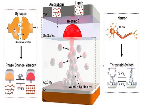 Neuromorphic Memory Device Simulates Neurons and Synapses
Simultaneous emulation of neuronal and synaptic properties promotes the development of brain-like artificial intelligence
Researchers have reported a nano-sized neuromorphic memory device that emulates neurons and synapses simultaneously in a unit cell, another step toward completing the goal of neuromorphic computing designed to rigorously mimic the human brain with semiconductor devices.
Neuromorphic computing aims to realize artificial intelligence (AI) by mimicking the mechanisms of neurons and synapses that make up the human brain. Inspired by the cognitive functions of the human brain that current computers cannot provide, neuromorphic devices have been widely investigated. However, current Complementary Metal-Oxide Semiconductor (CMOS)-based neuromorphic circuits simply connect artificial neurons and synapses without synergistic interactions, and the concomitant implementation of neurons and synapses still remains a challenge. To address these issues, a research team led by Professor Keon Jae Lee from the Department of Materials Science and Engineering implemented the biological working mechanisms of humans by introducing the neuron-synapse interactions in a single memory cell, rather than the conventional approach of electrically connecting artificial neuronal and synaptic devices.
Similar to commercial graphics cards, the artificial synaptic devices previously studied often used to accelerate parallel computations, which shows clear differences from the operational mechanisms of the human brain. The research team implemented the synergistic interactions between neurons and synapses in the neuromorphic memory device, emulating the mechanisms of the biological neural network. In addition, the developed neuromorphic device can replace complex CMOS neuron circuits with a single device, providing high scalability and cost efficiency.
The human brain consists of a complex network of 100 billion neurons and 100 trillion synapses. The functions and structures of neurons and synapses can flexibly change according to the external stimuli, adapting to the surrounding environment. The research team developed a neuromorphic device in which short-term and long-term memories coexist using volatile and non-volatile memory devices that mimic the characteristics of neurons and synapses, respectively. A threshold switch device is used as volatile memory and phase-change memory is used as a non-volatile device. Two thin-film devices are integrated without intermediate electrodes, implementing the functional adaptability of neurons and synapses in the neuromorphic memory.
Professor Keon Jae Lee explained, "Neurons and synapses interact with each other to establish cognitive functions such as memory and learning, so simulating both is an essential element for brain-inspired artificial intelligence. The developed neuromorphic memory device also mimics the retraining effect that allows quick learning of the forgotten information by implementing a positive feedback effect between neurons and synapses.”
This result entitled “Simultaneous emulation of synaptic and intrinsic plasticity using a memristive synapse” was published in the May 19, 2022 issue of Nature Communications.
-Publication:Sang Hyun Sung, Tae Jin Kim, Hyera Shin, Tae Hong Im, and Keon Jae Lee (2022) “Simultaneous emulation of synaptic and intrinsic plasticity using a memristive synapse,” Nature Communications May 19, 2022 (DOI: 10.1038/s41467-022-30432-2)
-Profile:Professor Keon Jae Leehttp://fand.kaist.ac.kr
Department of Materials Science and EngineeringKAIST
2022.05.20 View 15235
Neuromorphic Memory Device Simulates Neurons and Synapses
Simultaneous emulation of neuronal and synaptic properties promotes the development of brain-like artificial intelligence
Researchers have reported a nano-sized neuromorphic memory device that emulates neurons and synapses simultaneously in a unit cell, another step toward completing the goal of neuromorphic computing designed to rigorously mimic the human brain with semiconductor devices.
Neuromorphic computing aims to realize artificial intelligence (AI) by mimicking the mechanisms of neurons and synapses that make up the human brain. Inspired by the cognitive functions of the human brain that current computers cannot provide, neuromorphic devices have been widely investigated. However, current Complementary Metal-Oxide Semiconductor (CMOS)-based neuromorphic circuits simply connect artificial neurons and synapses without synergistic interactions, and the concomitant implementation of neurons and synapses still remains a challenge. To address these issues, a research team led by Professor Keon Jae Lee from the Department of Materials Science and Engineering implemented the biological working mechanisms of humans by introducing the neuron-synapse interactions in a single memory cell, rather than the conventional approach of electrically connecting artificial neuronal and synaptic devices.
Similar to commercial graphics cards, the artificial synaptic devices previously studied often used to accelerate parallel computations, which shows clear differences from the operational mechanisms of the human brain. The research team implemented the synergistic interactions between neurons and synapses in the neuromorphic memory device, emulating the mechanisms of the biological neural network. In addition, the developed neuromorphic device can replace complex CMOS neuron circuits with a single device, providing high scalability and cost efficiency.
The human brain consists of a complex network of 100 billion neurons and 100 trillion synapses. The functions and structures of neurons and synapses can flexibly change according to the external stimuli, adapting to the surrounding environment. The research team developed a neuromorphic device in which short-term and long-term memories coexist using volatile and non-volatile memory devices that mimic the characteristics of neurons and synapses, respectively. A threshold switch device is used as volatile memory and phase-change memory is used as a non-volatile device. Two thin-film devices are integrated without intermediate electrodes, implementing the functional adaptability of neurons and synapses in the neuromorphic memory.
Professor Keon Jae Lee explained, "Neurons and synapses interact with each other to establish cognitive functions such as memory and learning, so simulating both is an essential element for brain-inspired artificial intelligence. The developed neuromorphic memory device also mimics the retraining effect that allows quick learning of the forgotten information by implementing a positive feedback effect between neurons and synapses.”
This result entitled “Simultaneous emulation of synaptic and intrinsic plasticity using a memristive synapse” was published in the May 19, 2022 issue of Nature Communications.
-Publication:Sang Hyun Sung, Tae Jin Kim, Hyera Shin, Tae Hong Im, and Keon Jae Lee (2022) “Simultaneous emulation of synaptic and intrinsic plasticity using a memristive synapse,” Nature Communications May 19, 2022 (DOI: 10.1038/s41467-022-30432-2)
-Profile:Professor Keon Jae Leehttp://fand.kaist.ac.kr
Department of Materials Science and EngineeringKAIST
2022.05.20 View 15235 -
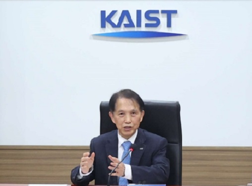 President Lee Presents Plans to Nurture Next-Generation Talents
President Lee stressed that nurturing medical scientists, semiconductor R&D personnel, startup entrepreneurs, and global innovators are key missions he will continue to pursue during a news conference
KAIST President Kwang Hyung Lee said that nurturing medical scientists, semiconductor R&D personnel, startup entrepreneurs, and global innovators are key missions he will continue to pursue during an online news conference marking the 1st anniversary of him becoming the president on February 15.
He said that nurturing physician-scientists is the most critical mission for KAIST to help the nation create a new growth engine. He said KAIST will help the nation drive the bio-industry and provide medical science resources for the nation’s health sector. To this end, he said that KAIST will open its Medical Science and Technology School by 2026.
“We plan to expand the current Graduate School of Medical Science and Engineering into a new Medical Science and Technology School that will focus entirely on a condensed MD-PhD course converging the fields of AI, bio, and physics,” he said.
The school aims to foster medical scientists whose research results will eventually be commercialized. He said that the university is now discussing revisions to related laws and regulations with the government and other universities.
To supply human resources to the semiconductor industry, President Lee said the university will add a campus in Pyongtaek City that will serve as an advanced convergence research hub in the field of next generation semiconductors in collaboration with Samsung Electronics and the city of Pyongtaek. The three-stage opening plan projected the final opening of the campus by 2036. During the first stage, which will be completed by 2026, it will construct the campus infrastructure in Pyongtaek city where Samsung Semiconductors runs two massive semiconductor complexes. By 2031, it plans to launch the open research platform including a future cities research center and future vehicles research center. The campus will open the global industrial collaboration cluster hub by 2036.
In the global arena, President Lee said he is working to open the New York campus with stakeholders in the United States. He announced the plan last December that was endorsed by New York-based entrepreneur Hee-Nam Bae, the chairman of Big Continent Inc. President Lee and Chairman Lee signed an MOU for the funding to open the campus in New York.
“We are discussing how to facilitate the plan and best accommodate the interests and potential of our students. Many ideas and plans are on the table and we think it will take longer than expected to finalize the plan,” explained President Lee.
However, he added that the basic idea is to offer art tech and health technology programs as well as an AI-based finance MBA at the New York campus, in addition to it serving as the startup accelerator of KAIST.
President Lee stressed the importance of technology commercialization when successfully launching KAIST Holdings last month to help spinoffs of KAIST labs accelerate their end results. He said that KAIST Holdings will build a virtuous supporting system to commercialize the technology startups coming from KAIST.
“We plan to list at least 10 KAIST startups on the KOSDAQ and two on the NASDAQ by 2031. KAIST Holdings also aims to nurture companies valued at a total of one billion KRW and earn 100 billion KRW in technology fees by 2031.
2022.02.17 View 12522
President Lee Presents Plans to Nurture Next-Generation Talents
President Lee stressed that nurturing medical scientists, semiconductor R&D personnel, startup entrepreneurs, and global innovators are key missions he will continue to pursue during a news conference
KAIST President Kwang Hyung Lee said that nurturing medical scientists, semiconductor R&D personnel, startup entrepreneurs, and global innovators are key missions he will continue to pursue during an online news conference marking the 1st anniversary of him becoming the president on February 15.
He said that nurturing physician-scientists is the most critical mission for KAIST to help the nation create a new growth engine. He said KAIST will help the nation drive the bio-industry and provide medical science resources for the nation’s health sector. To this end, he said that KAIST will open its Medical Science and Technology School by 2026.
“We plan to expand the current Graduate School of Medical Science and Engineering into a new Medical Science and Technology School that will focus entirely on a condensed MD-PhD course converging the fields of AI, bio, and physics,” he said.
The school aims to foster medical scientists whose research results will eventually be commercialized. He said that the university is now discussing revisions to related laws and regulations with the government and other universities.
To supply human resources to the semiconductor industry, President Lee said the university will add a campus in Pyongtaek City that will serve as an advanced convergence research hub in the field of next generation semiconductors in collaboration with Samsung Electronics and the city of Pyongtaek. The three-stage opening plan projected the final opening of the campus by 2036. During the first stage, which will be completed by 2026, it will construct the campus infrastructure in Pyongtaek city where Samsung Semiconductors runs two massive semiconductor complexes. By 2031, it plans to launch the open research platform including a future cities research center and future vehicles research center. The campus will open the global industrial collaboration cluster hub by 2036.
In the global arena, President Lee said he is working to open the New York campus with stakeholders in the United States. He announced the plan last December that was endorsed by New York-based entrepreneur Hee-Nam Bae, the chairman of Big Continent Inc. President Lee and Chairman Lee signed an MOU for the funding to open the campus in New York.
“We are discussing how to facilitate the plan and best accommodate the interests and potential of our students. Many ideas and plans are on the table and we think it will take longer than expected to finalize the plan,” explained President Lee.
However, he added that the basic idea is to offer art tech and health technology programs as well as an AI-based finance MBA at the New York campus, in addition to it serving as the startup accelerator of KAIST.
President Lee stressed the importance of technology commercialization when successfully launching KAIST Holdings last month to help spinoffs of KAIST labs accelerate their end results. He said that KAIST Holdings will build a virtuous supporting system to commercialize the technology startups coming from KAIST.
“We plan to list at least 10 KAIST startups on the KOSDAQ and two on the NASDAQ by 2031. KAIST Holdings also aims to nurture companies valued at a total of one billion KRW and earn 100 billion KRW in technology fees by 2031.
2022.02.17 View 12522 -
 A Team of Three PhD Candidates Wins the Korea Semiconductor Design Contest
“We felt a sense of responsibility to help the nation advance its semiconductor design technology”
A CMOS (complementary metal-oxide semiconductor)-based “ultra-low noise signal chip” for 6G communications designed by three PhD candidates at the KAIST School of Electrical Engineering won the Presidential Award at the 22nd Korea Semiconductor Design Contest.
The winners are PhD candidates Sun-Eui Park, Yoon-Seo Cho, and Ju-Eun Bang from the Integrated Circuits and System Lab run by Professor Jaehyouk Choi. The contest, which is hosted by the Ministry of Trade, Industry and Energy and the Korea Semiconductors Industry Association, is one of the top national semiconductor design contests for college students.
Park said the team felt a sense of responsibility to help advance semiconductor design technology in Korea when deciding to participate the contest. The team expressed deep gratitude to Professor Choi for guiding their research on 6G communications.
“Our colleagues from other labs and seniors who already graduated helped us a great deal, so we owe them a lot,” explained Park. Cho added that their hard work finally got recognized and that acknowledgement pushes her to move forward with her research. Meanwhile, Bang said she is delighted to see that many people seem to be interested in her research topic.
Research for 6G is attempting to reach 1 tera bps (Tbps), 50 times faster than 5G communications with transmission speeds of up to 20 gigabytes. In general, the wider the communication frequency band, the higher the data transmission speed. Thus, the use of frequency bands above 100 gigahertz is essential for delivering high data transmission speeds for 6G communications.
However, it remains a big challenge to make a precise benchmark signal that can be used as a carrier wave in a high frequency band. Despite the advantages of CMOS’s ultra-small and low-power design, it still has limitations at high frequency bands and its operating frequency. Thus, it was difficult to achieve a frequency band above 100 gigahertz.
To overcome these challenges, the three students introduced ultra-low noise signal generation technology that can support high-order modulation technologies. This technology is expected to contribute to increasing the price competitiveness and density of 6G communication chips that will be used in the future.
5G just got started in 2020 and still has long way to go for full commercialization. Nevertheless, many researchers have started preparing for 6G technology, targeting 2030 since a new cellular communication appears in every other decade.
Professor Choi said, “Generating ultra-high frequency signals in bands above 100 GHz with highly accurate timing is one of the key technologies for implementing 6G communication hardware. Our research is significant for the development of the world’s first semiconductor chip that will use the CMOS process to achieve noise performance of less than 80fs in a frequency band above 100 GHz.”
The team members plan to work as circuit designers in Korean semiconductor companies after graduation. “We will continue to research the development of signal generators on the topic of award-winning 6G. We would like to continue our research on high-speed circuit designs such as ultra-fast analog-to-digital converters,” Park added.
2021.11.30 View 10374
A Team of Three PhD Candidates Wins the Korea Semiconductor Design Contest
“We felt a sense of responsibility to help the nation advance its semiconductor design technology”
A CMOS (complementary metal-oxide semiconductor)-based “ultra-low noise signal chip” for 6G communications designed by three PhD candidates at the KAIST School of Electrical Engineering won the Presidential Award at the 22nd Korea Semiconductor Design Contest.
The winners are PhD candidates Sun-Eui Park, Yoon-Seo Cho, and Ju-Eun Bang from the Integrated Circuits and System Lab run by Professor Jaehyouk Choi. The contest, which is hosted by the Ministry of Trade, Industry and Energy and the Korea Semiconductors Industry Association, is one of the top national semiconductor design contests for college students.
Park said the team felt a sense of responsibility to help advance semiconductor design technology in Korea when deciding to participate the contest. The team expressed deep gratitude to Professor Choi for guiding their research on 6G communications.
“Our colleagues from other labs and seniors who already graduated helped us a great deal, so we owe them a lot,” explained Park. Cho added that their hard work finally got recognized and that acknowledgement pushes her to move forward with her research. Meanwhile, Bang said she is delighted to see that many people seem to be interested in her research topic.
Research for 6G is attempting to reach 1 tera bps (Tbps), 50 times faster than 5G communications with transmission speeds of up to 20 gigabytes. In general, the wider the communication frequency band, the higher the data transmission speed. Thus, the use of frequency bands above 100 gigahertz is essential for delivering high data transmission speeds for 6G communications.
However, it remains a big challenge to make a precise benchmark signal that can be used as a carrier wave in a high frequency band. Despite the advantages of CMOS’s ultra-small and low-power design, it still has limitations at high frequency bands and its operating frequency. Thus, it was difficult to achieve a frequency band above 100 gigahertz.
To overcome these challenges, the three students introduced ultra-low noise signal generation technology that can support high-order modulation technologies. This technology is expected to contribute to increasing the price competitiveness and density of 6G communication chips that will be used in the future.
5G just got started in 2020 and still has long way to go for full commercialization. Nevertheless, many researchers have started preparing for 6G technology, targeting 2030 since a new cellular communication appears in every other decade.
Professor Choi said, “Generating ultra-high frequency signals in bands above 100 GHz with highly accurate timing is one of the key technologies for implementing 6G communication hardware. Our research is significant for the development of the world’s first semiconductor chip that will use the CMOS process to achieve noise performance of less than 80fs in a frequency band above 100 GHz.”
The team members plan to work as circuit designers in Korean semiconductor companies after graduation. “We will continue to research the development of signal generators on the topic of award-winning 6G. We would like to continue our research on high-speed circuit designs such as ultra-fast analog-to-digital converters,” Park added.
2021.11.30 View 10374 -
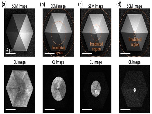 Quantum Emitters: Beyond Crystal Clear to Single-Photon Pure
‘Nanoscale Focus Pinspot’ can quench only the background noise without changing the optical properties of the quantum emitter and the built-in photonic structure
Photons, fundamental particles of light, are carrying these words to your eyes via the light from your computer screen or phone. Photons play a key role in the next-generation quantum information technology, such as quantum computing and communications. A quantum emitter, capable of producing a single, pure photon, is the crux of such technology but has many issues that have yet to be solved, according to KAIST researchers.
A research team under Professor Yong-Hoon Cho has developed a technique that can isolate the desired quality emitter by reducing the noise surrounding the target with what they have dubbed a ‘nanoscale focus pinspot.’ They published their results on June 24 in ACS Nano.
“The nanoscale focus pinspot is a structurally nondestructive technique under an extremely low dose ion beam and is generally applicable for various platforms to improve their single-photon purity while retaining the integrated photonic structures,” said lead author Yong-Hoon Cho from the Department of Physics at KAIST.
To produce single photons from solid state materials, the researchers used wide-bandgap semiconductor quantum dots — fabricated nanoparticles with specialized potential properties, such as the ability to directly inject current into a small chip and to operate at room temperature for practical applications. By making a quantum dot in a photonic structure that propagates light, and then irradiating it with helium ions, researchers theorized that they could develop a quantum emitter that could reduce the unwanted noisy background and produce a single, pure photon on demand.
Professor Cho explained, “Despite its high resolution and versatility, a focused ion beam typically suppresses the optical properties around the bombarded area due to the accelerated ion beam’s high momentum. We focused on the fact that, if the focused ion beam is well controlled, only the background noise can be selectively quenched with high spatial resolution without destroying the structure.”
In other words, the researchers focused the ion beam on a mere pin prick, effectively cutting off the interactions around the quantum dot and removing the physical properties that could negatively interact with and degrade the photon purity emitted from the quantum dot.
“It is the first developed technique that can quench the background noise without changing the optical properties of the quantum emitter and the built-in photonic structure,” Professor Cho asserted.
Professor Cho compared it to stimulated emission depletion microscopy, a technique used to decrease the light around the area of focus, but leaving the focal point illuminated. The result is increased resolution of the desired visual target.
“By adjusting the focused ion beam-irradiated region, we can select the target emitter with nanoscale resolution by quenching the surrounding emitter,” Professor Cho said. “This nanoscale selective-quenching technique can be applied to various material and structural platforms and further extended for applications such as optical memory and high-resolution micro displays.” Korea’s National Research Foundation and the Samsung Science and Technology Foundation supported this work.
-PublicationMinho Choi, Seongmoon Jun, and Yong-Hoon Cho et al. ACS Nano‘Nanoscale Focus Pinspot for High-Purity Quantum Emitters via Focused-Ion-Beam-Induced Luminescence Quenching,’(https://pubs.acs.org/doi/10.1021/acsnano.1c00587)
-ProfileProfessor Yong-Hoon ChoQuantum & Nanobio Photonics Laboratoryhttp://qnp.kaist.ac.kr/
Department of PhysicsKAIST
2021.09.02 View 12020
Quantum Emitters: Beyond Crystal Clear to Single-Photon Pure
‘Nanoscale Focus Pinspot’ can quench only the background noise without changing the optical properties of the quantum emitter and the built-in photonic structure
Photons, fundamental particles of light, are carrying these words to your eyes via the light from your computer screen or phone. Photons play a key role in the next-generation quantum information technology, such as quantum computing and communications. A quantum emitter, capable of producing a single, pure photon, is the crux of such technology but has many issues that have yet to be solved, according to KAIST researchers.
A research team under Professor Yong-Hoon Cho has developed a technique that can isolate the desired quality emitter by reducing the noise surrounding the target with what they have dubbed a ‘nanoscale focus pinspot.’ They published their results on June 24 in ACS Nano.
“The nanoscale focus pinspot is a structurally nondestructive technique under an extremely low dose ion beam and is generally applicable for various platforms to improve their single-photon purity while retaining the integrated photonic structures,” said lead author Yong-Hoon Cho from the Department of Physics at KAIST.
To produce single photons from solid state materials, the researchers used wide-bandgap semiconductor quantum dots — fabricated nanoparticles with specialized potential properties, such as the ability to directly inject current into a small chip and to operate at room temperature for practical applications. By making a quantum dot in a photonic structure that propagates light, and then irradiating it with helium ions, researchers theorized that they could develop a quantum emitter that could reduce the unwanted noisy background and produce a single, pure photon on demand.
Professor Cho explained, “Despite its high resolution and versatility, a focused ion beam typically suppresses the optical properties around the bombarded area due to the accelerated ion beam’s high momentum. We focused on the fact that, if the focused ion beam is well controlled, only the background noise can be selectively quenched with high spatial resolution without destroying the structure.”
In other words, the researchers focused the ion beam on a mere pin prick, effectively cutting off the interactions around the quantum dot and removing the physical properties that could negatively interact with and degrade the photon purity emitted from the quantum dot.
“It is the first developed technique that can quench the background noise without changing the optical properties of the quantum emitter and the built-in photonic structure,” Professor Cho asserted.
Professor Cho compared it to stimulated emission depletion microscopy, a technique used to decrease the light around the area of focus, but leaving the focal point illuminated. The result is increased resolution of the desired visual target.
“By adjusting the focused ion beam-irradiated region, we can select the target emitter with nanoscale resolution by quenching the surrounding emitter,” Professor Cho said. “This nanoscale selective-quenching technique can be applied to various material and structural platforms and further extended for applications such as optical memory and high-resolution micro displays.” Korea’s National Research Foundation and the Samsung Science and Technology Foundation supported this work.
-PublicationMinho Choi, Seongmoon Jun, and Yong-Hoon Cho et al. ACS Nano‘Nanoscale Focus Pinspot for High-Purity Quantum Emitters via Focused-Ion-Beam-Induced Luminescence Quenching,’(https://pubs.acs.org/doi/10.1021/acsnano.1c00587)
-ProfileProfessor Yong-Hoon ChoQuantum & Nanobio Photonics Laboratoryhttp://qnp.kaist.ac.kr/
Department of PhysicsKAIST
2021.09.02 View 12020 -
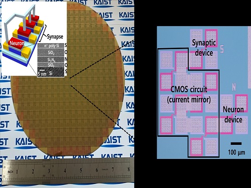 Brain-Inspired Highly Scalable Neuromorphic Hardware Presented
Neurons and synapses based on single transistor can dramatically reduce the hardware cost and accelerate the commercialization of neuromorphic hardware
KAIST researchers fabricated a brain-inspired highly scalable neuromorphic hardware by co-integrating single transistor neurons and synapses. Using standard silicon complementary metal-oxide-semiconductor (CMOS) technology, the neuromorphic hardware is expected to reduce chip cost and simplify fabrication procedures.
The research team led by Yang-Kyu Choi and Sung-Yool Choi produced a neurons and synapses based on single transistor for highly scalable neuromorphic hardware and showed the ability to recognize text and face images. This research was featured in Science Advances on August 4.
Neuromorphic hardware has attracted a great deal of attention because of its artificial intelligence functions, but consuming ultra-low power of less than 20 watts by mimicking the human brain. To make neuromorphic hardware work, a neuron that generates a spike when integrating a certain signal, and a synapse remembering the connection between two neurons are necessary, just like the biological brain. However, since neurons and synapses constructed on digital or analog circuits occupy a large space, there is a limit in terms of hardware efficiency and costs. Since the human brain consists of about 1011 neurons and 1014 synapses, it is necessary to improve the hardware cost in order to apply it to mobile and IoT devices.
To solve the problem, the research team mimicked the behavior of biological neurons and synapses with a single transistor, and co-integrated them onto an 8-inch wafer. The manufactured neuromorphic transistors have the same structure as the transistors for memory and logic that are currently mass-produced. In addition, the neuromorphic transistors proved for the first time that they can be implemented with a ‘Janus structure’ that functions as both neuron and synapse, just like coins have heads and tails.
Professor Yang-Kyu Choi said that this work can dramatically reduce the hardware cost by replacing the neurons and synapses that were based on complex digital and analog circuits with a single transistor. "We have demonstrated that neurons and synapses can be implemented using a single transistor," said Joon-Kyu Han, the first author. "By co-integrating single transistor neurons and synapses on the same wafer using a standard CMOS process, the hardware cost of the neuromorphic hardware has been improved, which will accelerate the commercialization of neuromorphic hardware,” Han added.This research was supported by the National Research Foundation (NRF) and IC Design Education Center (IDEC).
-PublicationJoon-Kyu Han, Sung-Yool Choi, Yang-Kyu Choi, et al.“Cointegration of single-transistor neurons and synapses by nanoscale CMOS fabrication for highly scalable neuromorphic hardware,” Science Advances (DOI: 10.1126/sciadv.abg8836)
-ProfileProfessor Yang-Kyu ChoiNano-Oriented Bio-Electronics Labhttps://sites.google.com/view/nobelab/
School of Electrical EngineeringKAIST
Professor Sung-Yool ChoiMolecular and Nano Device Laboratoryhttps://www.mndl.kaist.ac.kr/
School of Electrical EngineeringKAIST
2021.08.05 View 12397
Brain-Inspired Highly Scalable Neuromorphic Hardware Presented
Neurons and synapses based on single transistor can dramatically reduce the hardware cost and accelerate the commercialization of neuromorphic hardware
KAIST researchers fabricated a brain-inspired highly scalable neuromorphic hardware by co-integrating single transistor neurons and synapses. Using standard silicon complementary metal-oxide-semiconductor (CMOS) technology, the neuromorphic hardware is expected to reduce chip cost and simplify fabrication procedures.
The research team led by Yang-Kyu Choi and Sung-Yool Choi produced a neurons and synapses based on single transistor for highly scalable neuromorphic hardware and showed the ability to recognize text and face images. This research was featured in Science Advances on August 4.
Neuromorphic hardware has attracted a great deal of attention because of its artificial intelligence functions, but consuming ultra-low power of less than 20 watts by mimicking the human brain. To make neuromorphic hardware work, a neuron that generates a spike when integrating a certain signal, and a synapse remembering the connection between two neurons are necessary, just like the biological brain. However, since neurons and synapses constructed on digital or analog circuits occupy a large space, there is a limit in terms of hardware efficiency and costs. Since the human brain consists of about 1011 neurons and 1014 synapses, it is necessary to improve the hardware cost in order to apply it to mobile and IoT devices.
To solve the problem, the research team mimicked the behavior of biological neurons and synapses with a single transistor, and co-integrated them onto an 8-inch wafer. The manufactured neuromorphic transistors have the same structure as the transistors for memory and logic that are currently mass-produced. In addition, the neuromorphic transistors proved for the first time that they can be implemented with a ‘Janus structure’ that functions as both neuron and synapse, just like coins have heads and tails.
Professor Yang-Kyu Choi said that this work can dramatically reduce the hardware cost by replacing the neurons and synapses that were based on complex digital and analog circuits with a single transistor. "We have demonstrated that neurons and synapses can be implemented using a single transistor," said Joon-Kyu Han, the first author. "By co-integrating single transistor neurons and synapses on the same wafer using a standard CMOS process, the hardware cost of the neuromorphic hardware has been improved, which will accelerate the commercialization of neuromorphic hardware,” Han added.This research was supported by the National Research Foundation (NRF) and IC Design Education Center (IDEC).
-PublicationJoon-Kyu Han, Sung-Yool Choi, Yang-Kyu Choi, et al.“Cointegration of single-transistor neurons and synapses by nanoscale CMOS fabrication for highly scalable neuromorphic hardware,” Science Advances (DOI: 10.1126/sciadv.abg8836)
-ProfileProfessor Yang-Kyu ChoiNano-Oriented Bio-Electronics Labhttps://sites.google.com/view/nobelab/
School of Electrical EngineeringKAIST
Professor Sung-Yool ChoiMolecular and Nano Device Laboratoryhttps://www.mndl.kaist.ac.kr/
School of Electrical EngineeringKAIST
2021.08.05 View 12397 -
 Jungheung to Donate 30B KRW for Semiconductor Research and Education
Jungheung Group, a construction company in Korea, made a pledge to donate 30 billion KRW for semiconductor research and education at KAIST. Junghueng will spend 20 billion KRW to construct the semiconductor education and research facilities that will be established in Pyeongtaek City in collaboration with Samsung Electronics, and 10 billion will go for supporting the educational training program. The pledge ceremony was held at the Daejeon campus with Jungheung Group Chairman Chang-Sun Jung, KAIST President Kwang Hyung Lee, and Pyeongtaek City Mayor Jang-Seon Jung in attendance.
Chairman said, “The only way to earn a competitive edge in this era of technology hegemony is to invest in young talents in the science and technology fields. They will grow up to be excellent experts who will feed tens of thousands of people.” He added, “Donating to nurture future talents is the most rewarding investment we can make for the future.”
President Lee said, “Jungheung’s donation is an investment in the semiconductor industry in Korea, which will be the growth engine for the nation. We will make every effort to foster the world’s best workforce in the semiconductor sector.”
Mayor Jung also expressed high hopes for the advancement of KAIST into ‘Brain City,’ a complex designated with Samsung Electronics for the semiconductor industry.
“The city government will fully support the semiconductor industry and KAIST. In doing so, we look forward to becoming the center of the semiconductor industry in the nation,” announced Mayor Jung.
2021.07.20 View 6511
Jungheung to Donate 30B KRW for Semiconductor Research and Education
Jungheung Group, a construction company in Korea, made a pledge to donate 30 billion KRW for semiconductor research and education at KAIST. Junghueng will spend 20 billion KRW to construct the semiconductor education and research facilities that will be established in Pyeongtaek City in collaboration with Samsung Electronics, and 10 billion will go for supporting the educational training program. The pledge ceremony was held at the Daejeon campus with Jungheung Group Chairman Chang-Sun Jung, KAIST President Kwang Hyung Lee, and Pyeongtaek City Mayor Jang-Seon Jung in attendance.
Chairman said, “The only way to earn a competitive edge in this era of technology hegemony is to invest in young talents in the science and technology fields. They will grow up to be excellent experts who will feed tens of thousands of people.” He added, “Donating to nurture future talents is the most rewarding investment we can make for the future.”
President Lee said, “Jungheung’s donation is an investment in the semiconductor industry in Korea, which will be the growth engine for the nation. We will make every effort to foster the world’s best workforce in the semiconductor sector.”
Mayor Jung also expressed high hopes for the advancement of KAIST into ‘Brain City,’ a complex designated with Samsung Electronics for the semiconductor industry.
“The city government will fully support the semiconductor industry and KAIST. In doing so, we look forward to becoming the center of the semiconductor industry in the nation,” announced Mayor Jung.
2021.07.20 View 6511