quantum+dots
-
 Quantum Emitters: Beyond Crystal Clear to Single-Photon Pure
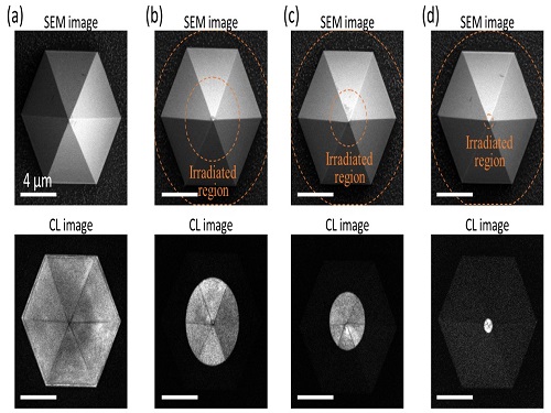
‘Nanoscale Focus Pinspot’ can quench only the background noise without changing the optical properties of the quantum emitter and the built-in photonic structure
Photons, fundamental particles of light, are carrying these words to your eyes via the light from your computer screen or phone. Photons play a key role in the next-generation quantum information technology, such as quantum computing and communications. A quantum emitter, capable of producing a single, pure photon, is the crux of such technology but has many issues that have yet to be solved, according to KAIST researchers.
A research team under Professor Yong-Hoon Cho has developed a technique that can isolate the desired quality emitter by reducing the noise surrounding the target with what they have dubbed a ‘nanoscale focus pinspot.’ They published their results on June 24 in ACS Nano.
“The nanoscale focus pinspot is a structurally nondestructive technique under an extremely low dose ion beam and is generally applicable for various platforms to improve their single-photon purity while retaining the integrated photonic structures,” said lead author Yong-Hoon Cho from the Department of Physics at KAIST.
To produce single photons from solid state materials, the researchers used wide-bandgap semiconductor quantum dots — fabricated nanoparticles with specialized potential properties, such as the ability to directly inject current into a small chip and to operate at room temperature for practical applications. By making a quantum dot in a photonic structure that propagates light, and then irradiating it with helium ions, researchers theorized that they could develop a quantum emitter that could reduce the unwanted noisy background and produce a single, pure photon on demand.
Professor Cho explained, “Despite its high resolution and versatility, a focused ion beam typically suppresses the optical properties around the bombarded area due to the accelerated ion beam’s high momentum. We focused on the fact that, if the focused ion beam is well controlled, only the background noise can be selectively quenched with high spatial resolution without destroying the structure.”
In other words, the researchers focused the ion beam on a mere pin prick, effectively cutting off the interactions around the quantum dot and removing the physical properties that could negatively interact with and degrade the photon purity emitted from the quantum dot.
“It is the first developed technique that can quench the background noise without changing the optical properties of the quantum emitter and the built-in photonic structure,” Professor Cho asserted.
Professor Cho compared it to stimulated emission depletion microscopy, a technique used to decrease the light around the area of focus, but leaving the focal point illuminated. The result is increased resolution of the desired visual target.
“By adjusting the focused ion beam-irradiated region, we can select the target emitter with nanoscale resolution by quenching the surrounding emitter,” Professor Cho said. “This nanoscale selective-quenching technique can be applied to various material and structural platforms and further extended for applications such as optical memory and high-resolution micro displays.” Korea’s National Research Foundation and the Samsung Science and Technology Foundation supported this work.
-PublicationMinho Choi, Seongmoon Jun, and Yong-Hoon Cho et al. ACS Nano‘Nanoscale Focus Pinspot for High-Purity Quantum Emitters via Focused-Ion-Beam-Induced Luminescence Quenching,’(https://pubs.acs.org/doi/10.1021/acsnano.1c00587)
-ProfileProfessor Yong-Hoon ChoQuantum & Nanobio Photonics Laboratoryhttp://qnp.kaist.ac.kr/
Department of PhysicsKAIST
2021.09.02 View 12864
 -
 Synthesizing Single-Crystalline Hexagonal Graphene Quantum Dots
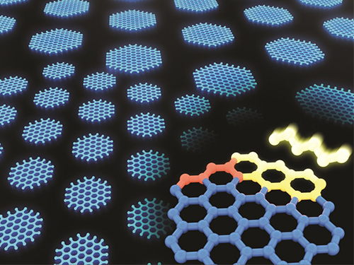
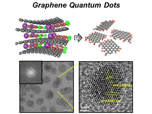
(Figure: Uniformly ordered single-crystalline graphene quantum dots of various sizes synthesized through solution chemistry.)
A KAIST team has designed a novel strategy for synthesizing single-crystalline graphene quantum dots, which emit stable blue light. The research team confirmed that a display made of their synthesized graphene quantum dots successfully emitted blue light with stable electric pressure, reportedly resolving the long-standing challenges of blue light emission in manufactured displays. The study, led by Professor O Ok Park in the Department of Chemical and Biological Engineering, was featured online in Nano Letters on July 5.
Graphene has gained increased attention as a next-generation material for its heat and electrical conductivity as well as its transparency. However, single and multi-layered graphene have characteristics of a conductor so that it is difficult to apply into semiconductor. Only when downsized to the nanoscale, semiconductor’s distinct feature of bandgap will be exhibited to emit the light in the graphene. This illuminating featuring of dot is referred to as a graphene quantum dot.
Conventionally, single-crystalline graphene has been fabricated by chemical vapor deposition (CVD) on copper or nickel thin films, or by peeling graphite physically and chemically. However, graphene made via chemical vapor deposition is mainly used for large-surface transparent electrodes. Meanwhile, graphene made by chemical and physical peeling carries uneven size defects.
The research team explained that their graphene quantum dots exhibited a very stable single-phase reaction when they mixed amine and acetic acid with an aqueous solution of glucose. Then, they synthesized single-crystalline graphene quantum dots from the self-assembly of the reaction intermediate. In the course of fabrication, the team developed a new separation method at a low-temperature precipitation, which led to successfully creating a homogeneous nucleation of graphene quantum dots via a single-phase reaction.
Professor Park and his colleagues have developed solution phase synthesis technology that allows for the creation of the desired crystal size for single nanocrystals down to 100 nano meters. It is reportedly the first synthesis of the homogeneous nucleation of graphene through a single-phase reaction.
Professor Park said, "This solution method will significantly contribute to the grafting of graphene in various fields. The application of this new graphene will expand the scope of its applications such as for flexible displays and varistors.”
This research was a joint project with a team from Korea University under Professor Sang Hyuk Im from the Department of Chemical and Biological Engineering, and was supported by the National Research Foundation of Korea, the Nano-Material Technology Development Program from the Electronics and Telecommunications Research Institute (ETRI), KAIST EEWS, and the BK21+ project from the Korean government.
2019.08.02 View 36375
 -
 Permanent, Wireless Self-charging System Using NIR Band
(Professor Jung-Yong Lee from the Graduate School of Energy, Environment, Water and Sustainability)
As wearable devices are emerging, there are numerous studies on wireless charging systems. Here, a KAIST research team has developed a permanent, wireless self-charging platform for low-power wearable electronics by converting near-infrared (NIR) band irradiation to electrical energy. This novel technology can be applied to flexible, wearable charging systems without needing any attachments.
Colloidal-quantum-dots (CQDs) are promising materials for manufacturing semiconductors; in particular, PbS-based CQDs have facile optical tunability from the visible to infrared wavelength region. Hence, they can be applied to various devices, such as lighting, photovoltaics (PVs), and photodetectors.
Continuous research on CQD-based optoelectronic devices has increased their power conversion efficiency (PCE) to 12%; however, applicable fields have not yet been found for them. Meanwhile, wearable electronic devices commonly face the problem of inconvenient charging systems because users have to constantly charge batteries attached to an energy source.
A joint team led by Professor Jung-Yong Lee from the Graduate School of Energy, Environment, Water and Sustainability and Jang Wok Choi from Seoul National University decided to apply CQD PVs, which have high quantum efficiency in NIR band to self-charging systems on wearable devices.
They employed a stable and efficient NIR energy conversion strategy. The system was comprised of a PbS CQD-based PV module, a flexible interdigitated lithium-ion battery, and various types of NIR-transparent films.
The team removed the existing battery from the already commercialized wearable healthcare bracelet and replaced it with the proposed self-charging system. They confirmed that the system can be applied to a low power wearable device via the NIR band.
There have been numerous platforms using solar irradiation, but the newly developed platform has more advantages because it allows conventional devices to be much more comfortable to wear and charged easily in everyday life using various irradiation sources for constant charging.
With this aspect, the proposed platform facilitates more flexible designs, which are the important component for actual commercialization. It also secures higher photostability and efficient than existing structures.
Professor Lee said, “By using the NIR band, we proposed a new approach to solve charging system issues of wearable devices. I believe that this platform will be a novel platform for energy conversion and that its application can be further extended to various fields, including mobiles, IoTs, and drones.”
This research, led by PhD Se-Woong Baek and M.S. candidate Jungmin Cho, was published in Advanced Materials on May 11.
Figure 1. a) Conceptual NIR-driven self-charging system including a flexible CQD PVs module and an interdigitatedly structured LIB. b) Photographic images of a conventional wearable healthcare bracelet and a self-charging system-integrated wearable device.
Figure 2. Illustration of the CQD PVs structure and performance of the wireless self-charging platform.
2018.10.08 View 9456
 -
 Improved Efficiency of CQD Solar Cells Using an Organic Thin Film
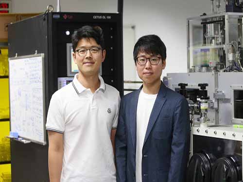
(from left: Professor Jung-Yong Lee and Dr. Se-Woong Baek)
Recently, the power conversion efficiency (PCE) of colloidal quantum dot (CQD)-based solar cells has been enhanced, paving the way for their commercialization in various fields; nevertheless, they are still a long way from being commercialized due to their efficiency not matching their stability. In this research, a KAIST team achieved highly stable and efficient CQD-based solar cells by using an amorphous organic layer to block oxygen and water permeation.
CQD-based solar cells are light-weight, flexible, and they boost light harvesting by absorbing near-infrared lights. Especially, they draw special attention for their optical properties controlled efficiently by changing the quantum dot sizes. However, they are still incompatible with existing solar cells in terms of efficiency, stability, and cost. Therefore, there is great demand for a novel technology that can simultaneously improve both PCE and stability while using an inexpensive electrode material.
Responding to this demand, Professor Jung-Yong Lee from the Graduate School of Energy, Environment, Water and Sustainability and his team introduced a technology to improve the efficiency and stability of CQD-based solar cells.
The team found that an amorphous organic thin film has a strong resistance to oxygen and water. Using these properties, they employed this doped organic layer as a top-hole selective layer (HSL) for the PbS CQD solar cells, and confirmed that the hydro/oxo-phobic properties of the layer efficiently protected the PbS layer. According to the molecular dynamics simulations, the layer significantly postponed the oxygen and water permeation into the PbS layer. Moreover, the efficient injection of the holes in the layer reduced interfacial resistance and improved performance.
With this technology, the team finally developed CQD-based solar cells with excellent stability. The PCE of their device stood at 11.7% and maintained over 90% of its initial performance when stored for one year under ambient conditions.
Professor Lee said, “This technology can be also applied to QD LEDs and Perovskite devices. I hope this technology can hasten the commercialization of CQD-based solar cells.”
This research, led by Dr. Se-Woong Baek and a Ph.D. student, Sang-Hoon Lee, was published in Energy & Environmental Science on May 10.
Figure 1. The schematic of the equilibrated structure of the amorphous organic film
Figure 2. Schematic illustration of CQD-based solar cells and graphs showing their performance
2018.08.27 View 9285
 -
 News Article on the Development of Synthesis Process for Graphene Quantum Dots
Before It's News, an international online news agency, highlighted the recent research conducted by KAIST professors (Seokwoo Jeon of the Department of Materials Science and Engineering, Yong-Hoon Cho of the Department of Physics, and Seunghyup Yoo of the Department of Electrical Engineering) on the development of synthesis process for graphene quantum dots, nanometer-sized round semiconductor nanoparticles that are very efficient at emitting photons. If commercialized, this synthetic technology will lead the way to the development of paper-thin displays in the future.
For the article, please go to the link below:
Before It’s News, September 3, 2014“Graphene quantum dots prove highly efficient in emitting light”
http://beforeitsnews.com/science-and-technology/2014/09/graphene-quantum-dots-prove-highly-efficient-in-emitting-light-2718190.html
2014.09.07 View 16080
 -
 Short Wavelength, Ultra-High Speed Quantum Light Source based on Quantum Dot Developed
Professor Yong Hoon, Cho (Department of Physics) and his research team synthesized an obelisk nanostructure and successfully formed a single semiconductor quantum exhibiting high reliability to realize an ultra-high speed, highly efficient, release of quantum dots.
The result of the research effort was published in the July 5th online edition of Scientific Reports published by Nature.
Semiconductor Quantum Dots restrict electrons within a cubic boundary of few nanometers thereby exhibiting similar properties to an atom with discontinuous energy levels. Exploitation of this characteristic makes possible the development of quantum light source, critical for next generation quantum information communication and quantum encryption.
High operational temperatures, stability, rapid photon release, electric current capability, and other advantages are reasons why semiconductor quantum dots are regarded as next generation core technology.
However conventional, spontaneously formed quantum dots are densely packed in a planar structure rendering the analysis of a single quantum dot difficult and result in the poor efficiency of photon release. In addition, the internal electromagnetic effect which is caused by inter-planar stress results in low internal quantum efficiency due to the difficulty in electron-hole recombination.
Professor Cho’s research team synthesized an obelisk shaped nanostructure using nitrides that emit short wavelengths of light. The activation layer was grown on the tip of the nanostructure and the team succeeded in placing a single quantum dot on the nano-tip. The team was therefore able to confirm the ultra-high speed single photon characteristics which occur at low energy levels.
Use of unique nanostructures makes synthesis of single atomic structures without processes like patterning while enabling the release of light emitted by the quantum dot.
Using this unique method the team showed the increase in internal quantum efficiency. The electromagnetic forces apparent in thin films no longer affects the quantum dot greatly due to the obelisk structure’s reduced inter planar stress.
The newly developed quantum light source emits visible light (400nm range) and not the conventional infrared light. This characteristic makes possible it use in communication in free space and enables use of highly efficient, visible range photon detector.
Professor Cho commented that “the developed method makes quantum dot growth much easier making single photon synthesis much faster to contribute to the development of practical quantum light source.” And that “the characteristics of the obelisk nanostructure enable the easy detachment from and attachment to other substrates enabling its use in producing single chip quantum light source.”
The research was conducted under the supervision of Professor Cho. The researchers werey Jae Hyung, Kim (first author) and Yong Ho, Ko (second author), both Ph.D. candidates at KAIST. The Ministry of Science, ICT and Future Planning, the National Research Foundation, and WCU Program provided support to the research effort.
2013.08.23 View 9710