photon
-
 KAIST achieves quantum entanglement essential for quantum error correction
Quantum computing is a technology capable of solving complex problems that classical computers struggle with. To perform accurate computations, quantum computers must correct errors that arise during operations. However, generating the quantum entanglement necessary for quantum error correction has long been considered a major challenge.
< Photo 1. (From left) Students Young-Do Yoon and Chan Roh of the Master's and Doctoral Integrated Program of the Department of Physics poses with Professor Young-Sik Ra and Student Geunhee Gwak of the same program >
KAIST (represented by President Kwang Hyung Lee) announced on the 25th of February that a research team led by Professor Young-Sik Ra from the Department of Physics has successfully implemented a three-dimensional cluster quantum entangled state, a key component for quantum error correction, through experimental demonstration.
Measurement-based quantum computing is an emerging paradigm that implements quantum computations by measuring specially entangled cluster states. The core of this approach lies in the generation of these cluster quantum entangled states, with two-dimensional cluster states commonly used for universal quantum computing.
However, to advance towards fault-tolerant quantum computing, which can correct quantum errors occurring during computations, a more complex three-dimensional cluster state is required. While previous studies have reported the generation of two-dimensional cluster states, experimental implementation of the three-dimensional cluster states necessary for fault-tolerant quantum computing had remained elusive due to the extreme complexity of their entanglement structure.
< Figure 1. (a) Experimental schematic. A pulse laser with a wavelength of 800 nm is converted into a pulse laser with a wavelength of 400 nm through second harmonic generation, and this is incident on a nonlinear crystal (PPKTP) to generate multiple quantum entanglement sources. (b) Generation of a 3D cluster state through optical mode basis change >
The research team overcame this challenge by developing a technique to control femtosecond time-frequency modes, successfully generating a three-dimensional cluster quantum entangled state for the first time.
The team directed a femtosecond laser into a nonlinear crystal, simultaneously generating quantum light sources across multiple frequency modes. (A femtosecond laser is a device that emits ultrashort, high-intensity light pulses.) Using this approach, they successfully created a three-dimensional cluster quantum entangled state.
Professor Young-Sik Ra noted, “This study marks the first successful demonstration of a three-dimensional cluster quantum entangled state, which was previously difficult to achieve with existing technology. This breakthrough is expected to serve as a crucial stepping stone for future research in measurement-based and fault-tolerant quantum computing.”
< Figure 2. Results of 3D cluster state generation. (a) Nullifier measurement of the cluster state. (b) 3D cluster state reconstructed using quantum state tomography. (c) Confirmation of quantum entanglement characteristics of the 3D cluster state >
The study was published online in Nature Photonics on February 24, 2025. The first author is Chan Roh, a Ph.D. candidate in KAIST’s integrated master’s and doctoral program, with Geunhee Gwak and Youngdo Yoon contributing as co-authors. (Paper title: “Generation of Three-Dimensional Cluster Entangled State”, DOI: 10.1038/s41566-025-01631-2)
This research was supported by the National Research Foundation of Korea (Quantum Computing Technology Development Program, Mid-Career Researcher Support Program, and Quantum Simulator for Materials Innovation Program), the Institute for Information & Communications Technology Planning & Evaluation (Quantum Internet Core Technology Program, University ICT Research Center Support Program), and the U.S. Air Force Research Laboratory.
2025.02.25 View 3300
KAIST achieves quantum entanglement essential for quantum error correction
Quantum computing is a technology capable of solving complex problems that classical computers struggle with. To perform accurate computations, quantum computers must correct errors that arise during operations. However, generating the quantum entanglement necessary for quantum error correction has long been considered a major challenge.
< Photo 1. (From left) Students Young-Do Yoon and Chan Roh of the Master's and Doctoral Integrated Program of the Department of Physics poses with Professor Young-Sik Ra and Student Geunhee Gwak of the same program >
KAIST (represented by President Kwang Hyung Lee) announced on the 25th of February that a research team led by Professor Young-Sik Ra from the Department of Physics has successfully implemented a three-dimensional cluster quantum entangled state, a key component for quantum error correction, through experimental demonstration.
Measurement-based quantum computing is an emerging paradigm that implements quantum computations by measuring specially entangled cluster states. The core of this approach lies in the generation of these cluster quantum entangled states, with two-dimensional cluster states commonly used for universal quantum computing.
However, to advance towards fault-tolerant quantum computing, which can correct quantum errors occurring during computations, a more complex three-dimensional cluster state is required. While previous studies have reported the generation of two-dimensional cluster states, experimental implementation of the three-dimensional cluster states necessary for fault-tolerant quantum computing had remained elusive due to the extreme complexity of their entanglement structure.
< Figure 1. (a) Experimental schematic. A pulse laser with a wavelength of 800 nm is converted into a pulse laser with a wavelength of 400 nm through second harmonic generation, and this is incident on a nonlinear crystal (PPKTP) to generate multiple quantum entanglement sources. (b) Generation of a 3D cluster state through optical mode basis change >
The research team overcame this challenge by developing a technique to control femtosecond time-frequency modes, successfully generating a three-dimensional cluster quantum entangled state for the first time.
The team directed a femtosecond laser into a nonlinear crystal, simultaneously generating quantum light sources across multiple frequency modes. (A femtosecond laser is a device that emits ultrashort, high-intensity light pulses.) Using this approach, they successfully created a three-dimensional cluster quantum entangled state.
Professor Young-Sik Ra noted, “This study marks the first successful demonstration of a three-dimensional cluster quantum entangled state, which was previously difficult to achieve with existing technology. This breakthrough is expected to serve as a crucial stepping stone for future research in measurement-based and fault-tolerant quantum computing.”
< Figure 2. Results of 3D cluster state generation. (a) Nullifier measurement of the cluster state. (b) 3D cluster state reconstructed using quantum state tomography. (c) Confirmation of quantum entanglement characteristics of the 3D cluster state >
The study was published online in Nature Photonics on February 24, 2025. The first author is Chan Roh, a Ph.D. candidate in KAIST’s integrated master’s and doctoral program, with Geunhee Gwak and Youngdo Yoon contributing as co-authors. (Paper title: “Generation of Three-Dimensional Cluster Entangled State”, DOI: 10.1038/s41566-025-01631-2)
This research was supported by the National Research Foundation of Korea (Quantum Computing Technology Development Program, Mid-Career Researcher Support Program, and Quantum Simulator for Materials Innovation Program), the Institute for Information & Communications Technology Planning & Evaluation (Quantum Internet Core Technology Program, University ICT Research Center Support Program), and the U.S. Air Force Research Laboratory.
2025.02.25 View 3300 -
 Ultralight advanced material developed by KAIST and U of Toronto
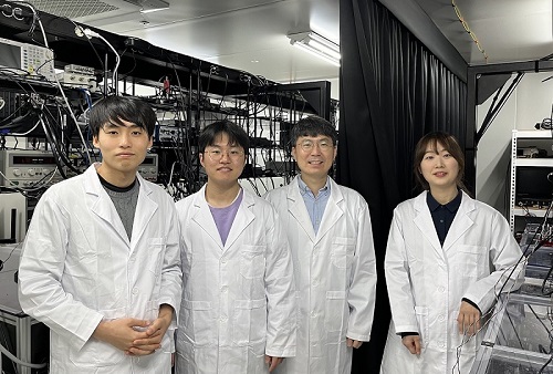
< (From left) Professor Seunghwa Ryu of KAIST Department of Mechanical Engineering, Professor Tobin Filleter of the University of Toronto, Dr. Jinwook Yeo of KAIST, and Dr. Peter Serles of the University of Toronto >
Recently, in advanced industries such as automobiles, aerospace, and mobility, there has been increasing demand for materials that achieve weight reduction while maintaining excellent mechanical properties. An international joint research team has developed an ultralight, high-strength material utilizing nanostructures, presenting the potential for various industrial applications through customized design in the future.
KAIST (represented by President Kwang Hyung Lee) announced on the 18th of February that a research team led by Professor Seunghwa Ryu from the Department of Mechanical Engineering, in collaboration with Professor Tobin Filleter from the University of Toronto, has developed a nano-lattice structure that maximizes lightweight properties while maintaining high stiffness and strength.
In this study, the research team optimized the beam shape of the lattice structure to maintain its lightweight characteristics while maximizing stiffness and strength.
Particularly, using a multi-objective Bayesian optimization algorithm*, the team conducted an optimal design process that simultaneously considers tensile and shear stiffness improvement and weight reduction. They demonstrated that the optimal lattice structure could be predicted and designed with significantly less data (about 400 data points) compared to conventional methods.
*Multi-objective Bayesian optimization algorithm: A method that finds the optimal solution while considering multiple objectives simultaneously. It efficiently collects data and predicts results even under conditions of uncertainty.
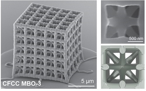
< Figure 1. Multi-objective Bayesian optimization for generative design of carbon nanolattices with high compressive stiffness and strength at low density. The upper is the illustration of process workflow. The lower part shows top four MBO CFCC geometries with their 2D Bézier curves. (The optimized structure is predicted and designed with much less data (approximately 400) than the conventional method >
Furthermore, to maximize the effect where mechanical properties improve as size decreases at the nanoscale, the research team utilized pyrolytic carbon* material to implement an ultralight, high-strength, high-stiffness nano-lattice structure.
*Pyrolytic carbon: A carbon material obtained by decomposing organic substances at high temperatures. It has excellent heat resistance and strength, making it widely used in industries such as semiconductor equipment coatings and artificial joint coatings, where it must withstand high temperatures without deformation.
For this, the team applied two-photon polymerization (2PP) technology* to precisely fabricate complex nano-lattice structures, and mechanical performance evaluations confirmed that the developed structure simultaneously possesses strength comparable to steel and the lightness of Styrofoam.
*Two-photon polymerization (2PP) technology: An advanced optical manufacturing technique based on the principle that polymerization occurs only when two photons of a specific wavelength are absorbed simultaneously.
Additionally, the research team demonstrated that multi-focus two-photon polymerization (multi-focus 2PP) technology enables the fabrication of millimeter-scale structures while maintaining nanoscale precision.
Professor Seunghwa Ryu explained, "This technology innovatively solves the stress concentration issue, which has been a limitation of conventional design methods, through three-dimensional nano-lattice structures, achieving both ultralight weight and high strength in material development."
< Figure 2. FESEM image of the fabricated nano-lattice structure and (bottom right) the macroscopic nanolattice resting on a bubble >
He further emphasized, "By integrating data-driven optimal design with precision 3D printing technology, this development not only meets the demand for lightweight materials in the aerospace and automotive industries but also opens possibilities for various industrial applications through customized design."
This study was led by Dr. Peter Serles of the Department of Mechanical & Industrial Engineering at University of Toronto and Dr. Jinwook Yeo from KAIST as co-first authors, with Professor Seunghwa Ryu and Professor Tobin Filleter as corresponding authors.
The research was published on January 23, 2025 in the international journal Advanced Materials (Paper title: “Ultrahigh Specific Strength by Bayesian Optimization of Lightweight Carbon Nanolattices”).
DOI: https://doi.org/10.1002/adma.202410651
This research was supported by the Multiphase Materials Innovation Manufacturing Research Center (an ERC program) funded by the Ministry of Science and ICT, the M3DT (Medical Device Digital Development Tool) project funded by the Ministry of Food and Drug Safety, and the KAIST International Collaboration Program.
2025.02.18 View 5046
Ultralight advanced material developed by KAIST and U of Toronto
< (From left) Professor Seunghwa Ryu of KAIST Department of Mechanical Engineering, Professor Tobin Filleter of the University of Toronto, Dr. Jinwook Yeo of KAIST, and Dr. Peter Serles of the University of Toronto >
Recently, in advanced industries such as automobiles, aerospace, and mobility, there has been increasing demand for materials that achieve weight reduction while maintaining excellent mechanical properties. An international joint research team has developed an ultralight, high-strength material utilizing nanostructures, presenting the potential for various industrial applications through customized design in the future.
KAIST (represented by President Kwang Hyung Lee) announced on the 18th of February that a research team led by Professor Seunghwa Ryu from the Department of Mechanical Engineering, in collaboration with Professor Tobin Filleter from the University of Toronto, has developed a nano-lattice structure that maximizes lightweight properties while maintaining high stiffness and strength.
In this study, the research team optimized the beam shape of the lattice structure to maintain its lightweight characteristics while maximizing stiffness and strength.
Particularly, using a multi-objective Bayesian optimization algorithm*, the team conducted an optimal design process that simultaneously considers tensile and shear stiffness improvement and weight reduction. They demonstrated that the optimal lattice structure could be predicted and designed with significantly less data (about 400 data points) compared to conventional methods.
*Multi-objective Bayesian optimization algorithm: A method that finds the optimal solution while considering multiple objectives simultaneously. It efficiently collects data and predicts results even under conditions of uncertainty.
< Figure 1. Multi-objective Bayesian optimization for generative design of carbon nanolattices with high compressive stiffness and strength at low density. The upper is the illustration of process workflow. The lower part shows top four MBO CFCC geometries with their 2D Bézier curves. (The optimized structure is predicted and designed with much less data (approximately 400) than the conventional method >
Furthermore, to maximize the effect where mechanical properties improve as size decreases at the nanoscale, the research team utilized pyrolytic carbon* material to implement an ultralight, high-strength, high-stiffness nano-lattice structure.
*Pyrolytic carbon: A carbon material obtained by decomposing organic substances at high temperatures. It has excellent heat resistance and strength, making it widely used in industries such as semiconductor equipment coatings and artificial joint coatings, where it must withstand high temperatures without deformation.
For this, the team applied two-photon polymerization (2PP) technology* to precisely fabricate complex nano-lattice structures, and mechanical performance evaluations confirmed that the developed structure simultaneously possesses strength comparable to steel and the lightness of Styrofoam.
*Two-photon polymerization (2PP) technology: An advanced optical manufacturing technique based on the principle that polymerization occurs only when two photons of a specific wavelength are absorbed simultaneously.
Additionally, the research team demonstrated that multi-focus two-photon polymerization (multi-focus 2PP) technology enables the fabrication of millimeter-scale structures while maintaining nanoscale precision.
Professor Seunghwa Ryu explained, "This technology innovatively solves the stress concentration issue, which has been a limitation of conventional design methods, through three-dimensional nano-lattice structures, achieving both ultralight weight and high strength in material development."
< Figure 2. FESEM image of the fabricated nano-lattice structure and (bottom right) the macroscopic nanolattice resting on a bubble >
He further emphasized, "By integrating data-driven optimal design with precision 3D printing technology, this development not only meets the demand for lightweight materials in the aerospace and automotive industries but also opens possibilities for various industrial applications through customized design."
This study was led by Dr. Peter Serles of the Department of Mechanical & Industrial Engineering at University of Toronto and Dr. Jinwook Yeo from KAIST as co-first authors, with Professor Seunghwa Ryu and Professor Tobin Filleter as corresponding authors.
The research was published on January 23, 2025 in the international journal Advanced Materials (Paper title: “Ultrahigh Specific Strength by Bayesian Optimization of Lightweight Carbon Nanolattices”).
DOI: https://doi.org/10.1002/adma.202410651
This research was supported by the Multiphase Materials Innovation Manufacturing Research Center (an ERC program) funded by the Ministry of Science and ICT, the M3DT (Medical Device Digital Development Tool) project funded by the Ministry of Food and Drug Safety, and the KAIST International Collaboration Program.
2025.02.18 View 5046 -
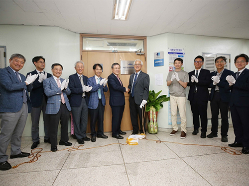
 KAIST to begin Joint Research to Develop Next-Generation LiDAR System with Hyundai Motor Group
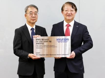
< (From left) Jong-Soo Lee, Executive Vice President at Hyundai Motor, Sang-Yup Lee, Senior Vice President for Research at KAIST >
The ‘Hyundai Motor Group-KAIST On-Chip LiDAR Joint Research Lab’ was opened at KAIST’s main campus in Daejeon to develop LiDAR sensors for advanced autonomous vehicles.
The joint research lab aims to develop high-performance and compact on-chip sensors and new signal detection technology, which are essential in the increasingly competitive autonomous driving market. On-chip sensors, which utilize semiconductor manufacturing technology to add various functions, can reduce the size of LiDAR systems compared to conventional methods and secure price competitiveness through mass production using semiconductor fabrication processes.
The joint research lab will consist of about 30 researchers, including the Hyundai-Kia Institute of Advanced Technology Development research team and KAIST professors Sanghyeon Kim, Sangsik Kim, Wanyeong Jung, and Hamza Kurt from KAIST’s School of Electrical Engineering, and will operate for four years until 2028.
KAIST will be leading the specialized work of each research team, such as for the development of silicon optoelectronic on-chip LiDAR components, the fabrication of high-speed, high-power integrated circuits to run the LiDAR systems, and the optimization and verification of LiDAR systems.
Hyundai Motor and Kia, together with Hyundai NGV, a specialized industry-academia cooperation institution, will oversee the operation of the joint research lab and provide support such as monitoring technological trends, suggesting research directions, deriving core ideas, and recommending technologies and experts to enhance research capabilities.
A Hyundai Motor Group official said, "We believe that this cooperation between Hyundai Motor Company and Kia, the leader in autonomous driving technology, and KAIST, the home of world-class technology, will hasten the achievement of fully autonomous driving." He added, "We will do our best to enable the lab to produce tangible results.”
Professor Sanghyeon Kim said, "The LiDAR sensor, which serves as the eyes of a car, is a core technology for future autonomous vehicle development that is essential for automobile companies to internalize."
2024.02.27 View 11310
KAIST to begin Joint Research to Develop Next-Generation LiDAR System with Hyundai Motor Group
< (From left) Jong-Soo Lee, Executive Vice President at Hyundai Motor, Sang-Yup Lee, Senior Vice President for Research at KAIST >
The ‘Hyundai Motor Group-KAIST On-Chip LiDAR Joint Research Lab’ was opened at KAIST’s main campus in Daejeon to develop LiDAR sensors for advanced autonomous vehicles.
The joint research lab aims to develop high-performance and compact on-chip sensors and new signal detection technology, which are essential in the increasingly competitive autonomous driving market. On-chip sensors, which utilize semiconductor manufacturing technology to add various functions, can reduce the size of LiDAR systems compared to conventional methods and secure price competitiveness through mass production using semiconductor fabrication processes.
The joint research lab will consist of about 30 researchers, including the Hyundai-Kia Institute of Advanced Technology Development research team and KAIST professors Sanghyeon Kim, Sangsik Kim, Wanyeong Jung, and Hamza Kurt from KAIST’s School of Electrical Engineering, and will operate for four years until 2028.
KAIST will be leading the specialized work of each research team, such as for the development of silicon optoelectronic on-chip LiDAR components, the fabrication of high-speed, high-power integrated circuits to run the LiDAR systems, and the optimization and verification of LiDAR systems.
Hyundai Motor and Kia, together with Hyundai NGV, a specialized industry-academia cooperation institution, will oversee the operation of the joint research lab and provide support such as monitoring technological trends, suggesting research directions, deriving core ideas, and recommending technologies and experts to enhance research capabilities.
A Hyundai Motor Group official said, "We believe that this cooperation between Hyundai Motor Company and Kia, the leader in autonomous driving technology, and KAIST, the home of world-class technology, will hasten the achievement of fully autonomous driving." He added, "We will do our best to enable the lab to produce tangible results.”
Professor Sanghyeon Kim said, "The LiDAR sensor, which serves as the eyes of a car, is a core technology for future autonomous vehicle development that is essential for automobile companies to internalize."
2024.02.27 View 11310 -
 A KAIST research team unveils new path for dense photonic integration
Integrated optical semiconductor (hereinafter referred to as optical semiconductor) technology is a next-generation semiconductor technology for which many researches and investments are being made worldwide because it can make complex optical systems such as LiDAR and quantum sensors and computers into a single small chip. In the existing semiconductor technology, the key was how small it was to make it in units of 5 nanometers or 2 nanometers, but increasing the degree of integration in optical semiconductor devices can be said to be a key technology that determines performance, price, and energy efficiency.
KAIST (President Kwang-Hyung Lee) announced on the 19th that a research team led by Professor Sangsik Kim of the Department of Electrical and Electronic Engineering discovered a new optical coupling mechanism that can increase the degree of integration of optical semiconductor devices by more than 100 times.
The degree of the number of elements that can be configured per chip is called the degree of integration. However, it is very difficult to increase the degree of integration of optical semiconductor devices, because crosstalk occurs between photons between adjacent devices due to the wave nature of light.
In previous studies, it was possible to reduce crosstalk of light only in specific polarizations, but in this study, the research team developed a method to increase the degree of integration even under polarization conditions, which were previously considered impossible, by discovering a new light coupling mechanism.
This study, led by Professor Sangsik Kim as a corresponding author and conducted with students he taught at Texas Tech University, was published in the international journal 'Light: Science & Applications' [IF=20.257] on June 2nd. done. (Paper title: Anisotropic leaky-like perturbation with subwavelength gratings enables zero crosstalk).
Professor Sangsik Kim said, "The interesting thing about this study is that it paradoxically eliminated the confusion through leaky waves (light tends to spread sideways), which was previously thought to increase the crosstalk." He went on to add, “If the optical coupling method using the leaky wave revealed in this study is applied, it will be possible to develop various optical semiconductor devices that are smaller and that has less noise.”
Professor Sangsik Kim is a researcher recognized for his expertise and research in optical semiconductor integration. Through his previous research, he developed an all-dielectric metamaterial that can control the degree of light spreading laterally by patterning a semiconductor structure at a size smaller than the wavelength, and proved this through experiments to improve the degree of integration of optical semiconductors. These studies were reported in ‘Nature Communications’ (Vol. 9, Article 1893, 2018) and ‘Optica’ (Vol. 7, pp. 881-887, 2020). In recognition of these achievements, Professor Kim has received the NSF Career Award from the National Science Foundation (NSF) and the Young Scientist Award from the Association of Korean-American Scientists and Engineers.
Meanwhile, this research was carried out with the support from the New Research Project of Excellence of the National Research Foundation of Korea and and the National Science Foundation of the US.
< Figure 1. Illustration depicting light propagation without crosstalk in the waveguide array of the developed metamaterial-based optical semiconductor >
2023.06.21 View 8472
A KAIST research team unveils new path for dense photonic integration
Integrated optical semiconductor (hereinafter referred to as optical semiconductor) technology is a next-generation semiconductor technology for which many researches and investments are being made worldwide because it can make complex optical systems such as LiDAR and quantum sensors and computers into a single small chip. In the existing semiconductor technology, the key was how small it was to make it in units of 5 nanometers or 2 nanometers, but increasing the degree of integration in optical semiconductor devices can be said to be a key technology that determines performance, price, and energy efficiency.
KAIST (President Kwang-Hyung Lee) announced on the 19th that a research team led by Professor Sangsik Kim of the Department of Electrical and Electronic Engineering discovered a new optical coupling mechanism that can increase the degree of integration of optical semiconductor devices by more than 100 times.
The degree of the number of elements that can be configured per chip is called the degree of integration. However, it is very difficult to increase the degree of integration of optical semiconductor devices, because crosstalk occurs between photons between adjacent devices due to the wave nature of light.
In previous studies, it was possible to reduce crosstalk of light only in specific polarizations, but in this study, the research team developed a method to increase the degree of integration even under polarization conditions, which were previously considered impossible, by discovering a new light coupling mechanism.
This study, led by Professor Sangsik Kim as a corresponding author and conducted with students he taught at Texas Tech University, was published in the international journal 'Light: Science & Applications' [IF=20.257] on June 2nd. done. (Paper title: Anisotropic leaky-like perturbation with subwavelength gratings enables zero crosstalk).
Professor Sangsik Kim said, "The interesting thing about this study is that it paradoxically eliminated the confusion through leaky waves (light tends to spread sideways), which was previously thought to increase the crosstalk." He went on to add, “If the optical coupling method using the leaky wave revealed in this study is applied, it will be possible to develop various optical semiconductor devices that are smaller and that has less noise.”
Professor Sangsik Kim is a researcher recognized for his expertise and research in optical semiconductor integration. Through his previous research, he developed an all-dielectric metamaterial that can control the degree of light spreading laterally by patterning a semiconductor structure at a size smaller than the wavelength, and proved this through experiments to improve the degree of integration of optical semiconductors. These studies were reported in ‘Nature Communications’ (Vol. 9, Article 1893, 2018) and ‘Optica’ (Vol. 7, pp. 881-887, 2020). In recognition of these achievements, Professor Kim has received the NSF Career Award from the National Science Foundation (NSF) and the Young Scientist Award from the Association of Korean-American Scientists and Engineers.
Meanwhile, this research was carried out with the support from the New Research Project of Excellence of the National Research Foundation of Korea and and the National Science Foundation of the US.
< Figure 1. Illustration depicting light propagation without crosstalk in the waveguide array of the developed metamaterial-based optical semiconductor >
2023.06.21 View 8472 -
 Eco-Friendly Micro-Supercapacitors Using Fallen Leaves
Green micro-supercapacitors on a single leaf could easily be applied in wearable electronics, smart houses, and IoTs
A KAIST research team has developed graphene-inorganic-hybrid micro-supercapacitors made of fallen leaves using femtosecond laser direct writing. The rapid development of wearable electronics requires breakthrough innovations in flexible energy storage devices in which micro-supercapacitors have drawn a great deal of interest due to their high power density, long lifetimes, and short charging times. Recently, there has been an enormous increase in waste batteries owing to the growing demand and the shortened replacement cycle in consumer electronics. The safety and environmental issues involved in the collection, recycling, and processing of such waste batteries are creating a number of challenges.
Forests cover about 30 percent of the Earth’s surface and produce a huge amount of fallen leaves. This naturally occurring biomass comes in large quantities and is completely biodegradable, which makes it an attractive sustainable resource. Nevertheless, if the fallen leaves are left neglected instead of being used efficiently, they can contribute to fire hazards, air pollution, and global warming.
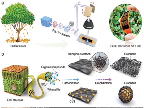
To solve both problems at once, a research team led by Professor Young-Jin Kim from the Department of Mechanical Engineering and Dr. Hana Yoon from the Korea Institute of Energy Research developed a novel technology that can create 3D porous graphene microelectrodes with high electrical conductivity by irradiating femtosecond laser pulses on the leaves in ambient air. This one-step fabrication does not require any additional materials or pre-treatment.
They showed that this technique could quickly and easily produce porous graphene electrodes at a low price, and demonstrated potential applications by fabricating graphene micro-supercapacitors to power an LED and an electronic watch. These results open up a new possibility for the mass production of flexible and green graphene-based electronic devices.
Professor Young-Jin Kim said, “Leaves create forest biomass that comes in unmanageable quantities, so using them for next-generation energy storage devices makes it possible for us to reuse waste resources, thereby establishing a virtuous cycle.”
This research was published in Advanced Functional Materials last month and was sponsored by the Ministry of Agriculture Food and Rural Affairs, the Korea Forest Service, and the Korea Institute of Energy Research.
-Publication
Truong-Son Dinh Le, Yeong A. Lee, Han Ku Nam, Kyu Yeon Jang, Dongwook Yang, Byunggi Kim, Kanghoon Yim, Seung Woo Kim, Hana Yoon, and Young-jin Kim, “Green Flexible Graphene-Inorganic-Hybrid Micro-Supercapacitors Made of Fallen Leaves Enabled by Ultrafast Laser Pulses," December 05, 2021, Advanced Functional Materials (doi.org/10.1002/adfm.202107768)
-ProfileProfessor Young-Jin KimUltra-Precision Metrology and Manufacturing (UPM2) LaboratoryDepartment of Mechanical EngineeringKAIST
2022.01.27 View 13943
Eco-Friendly Micro-Supercapacitors Using Fallen Leaves
Green micro-supercapacitors on a single leaf could easily be applied in wearable electronics, smart houses, and IoTs
A KAIST research team has developed graphene-inorganic-hybrid micro-supercapacitors made of fallen leaves using femtosecond laser direct writing. The rapid development of wearable electronics requires breakthrough innovations in flexible energy storage devices in which micro-supercapacitors have drawn a great deal of interest due to their high power density, long lifetimes, and short charging times. Recently, there has been an enormous increase in waste batteries owing to the growing demand and the shortened replacement cycle in consumer electronics. The safety and environmental issues involved in the collection, recycling, and processing of such waste batteries are creating a number of challenges.
Forests cover about 30 percent of the Earth’s surface and produce a huge amount of fallen leaves. This naturally occurring biomass comes in large quantities and is completely biodegradable, which makes it an attractive sustainable resource. Nevertheless, if the fallen leaves are left neglected instead of being used efficiently, they can contribute to fire hazards, air pollution, and global warming.
To solve both problems at once, a research team led by Professor Young-Jin Kim from the Department of Mechanical Engineering and Dr. Hana Yoon from the Korea Institute of Energy Research developed a novel technology that can create 3D porous graphene microelectrodes with high electrical conductivity by irradiating femtosecond laser pulses on the leaves in ambient air. This one-step fabrication does not require any additional materials or pre-treatment.
They showed that this technique could quickly and easily produce porous graphene electrodes at a low price, and demonstrated potential applications by fabricating graphene micro-supercapacitors to power an LED and an electronic watch. These results open up a new possibility for the mass production of flexible and green graphene-based electronic devices.
Professor Young-Jin Kim said, “Leaves create forest biomass that comes in unmanageable quantities, so using them for next-generation energy storage devices makes it possible for us to reuse waste resources, thereby establishing a virtuous cycle.”
This research was published in Advanced Functional Materials last month and was sponsored by the Ministry of Agriculture Food and Rural Affairs, the Korea Forest Service, and the Korea Institute of Energy Research.
-Publication
Truong-Son Dinh Le, Yeong A. Lee, Han Ku Nam, Kyu Yeon Jang, Dongwook Yang, Byunggi Kim, Kanghoon Yim, Seung Woo Kim, Hana Yoon, and Young-jin Kim, “Green Flexible Graphene-Inorganic-Hybrid Micro-Supercapacitors Made of Fallen Leaves Enabled by Ultrafast Laser Pulses," December 05, 2021, Advanced Functional Materials (doi.org/10.1002/adfm.202107768)
-ProfileProfessor Young-Jin KimUltra-Precision Metrology and Manufacturing (UPM2) LaboratoryDepartment of Mechanical EngineeringKAIST
2022.01.27 View 13943 -
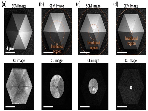 Quantum Emitters: Beyond Crystal Clear to Single-Photon Pure
‘Nanoscale Focus Pinspot’ can quench only the background noise without changing the optical properties of the quantum emitter and the built-in photonic structure
Photons, fundamental particles of light, are carrying these words to your eyes via the light from your computer screen or phone. Photons play a key role in the next-generation quantum information technology, such as quantum computing and communications. A quantum emitter, capable of producing a single, pure photon, is the crux of such technology but has many issues that have yet to be solved, according to KAIST researchers.
A research team under Professor Yong-Hoon Cho has developed a technique that can isolate the desired quality emitter by reducing the noise surrounding the target with what they have dubbed a ‘nanoscale focus pinspot.’ They published their results on June 24 in ACS Nano.
“The nanoscale focus pinspot is a structurally nondestructive technique under an extremely low dose ion beam and is generally applicable for various platforms to improve their single-photon purity while retaining the integrated photonic structures,” said lead author Yong-Hoon Cho from the Department of Physics at KAIST.
To produce single photons from solid state materials, the researchers used wide-bandgap semiconductor quantum dots — fabricated nanoparticles with specialized potential properties, such as the ability to directly inject current into a small chip and to operate at room temperature for practical applications. By making a quantum dot in a photonic structure that propagates light, and then irradiating it with helium ions, researchers theorized that they could develop a quantum emitter that could reduce the unwanted noisy background and produce a single, pure photon on demand.
Professor Cho explained, “Despite its high resolution and versatility, a focused ion beam typically suppresses the optical properties around the bombarded area due to the accelerated ion beam’s high momentum. We focused on the fact that, if the focused ion beam is well controlled, only the background noise can be selectively quenched with high spatial resolution without destroying the structure.”
In other words, the researchers focused the ion beam on a mere pin prick, effectively cutting off the interactions around the quantum dot and removing the physical properties that could negatively interact with and degrade the photon purity emitted from the quantum dot.
“It is the first developed technique that can quench the background noise without changing the optical properties of the quantum emitter and the built-in photonic structure,” Professor Cho asserted.
Professor Cho compared it to stimulated emission depletion microscopy, a technique used to decrease the light around the area of focus, but leaving the focal point illuminated. The result is increased resolution of the desired visual target.
“By adjusting the focused ion beam-irradiated region, we can select the target emitter with nanoscale resolution by quenching the surrounding emitter,” Professor Cho said. “This nanoscale selective-quenching technique can be applied to various material and structural platforms and further extended for applications such as optical memory and high-resolution micro displays.” Korea’s National Research Foundation and the Samsung Science and Technology Foundation supported this work.
-PublicationMinho Choi, Seongmoon Jun, and Yong-Hoon Cho et al. ACS Nano‘Nanoscale Focus Pinspot for High-Purity Quantum Emitters via Focused-Ion-Beam-Induced Luminescence Quenching,’(https://pubs.acs.org/doi/10.1021/acsnano.1c00587)
-ProfileProfessor Yong-Hoon ChoQuantum & Nanobio Photonics Laboratoryhttp://qnp.kaist.ac.kr/
Department of PhysicsKAIST
2021.09.02 View 12148
Quantum Emitters: Beyond Crystal Clear to Single-Photon Pure
‘Nanoscale Focus Pinspot’ can quench only the background noise without changing the optical properties of the quantum emitter and the built-in photonic structure
Photons, fundamental particles of light, are carrying these words to your eyes via the light from your computer screen or phone. Photons play a key role in the next-generation quantum information technology, such as quantum computing and communications. A quantum emitter, capable of producing a single, pure photon, is the crux of such technology but has many issues that have yet to be solved, according to KAIST researchers.
A research team under Professor Yong-Hoon Cho has developed a technique that can isolate the desired quality emitter by reducing the noise surrounding the target with what they have dubbed a ‘nanoscale focus pinspot.’ They published their results on June 24 in ACS Nano.
“The nanoscale focus pinspot is a structurally nondestructive technique under an extremely low dose ion beam and is generally applicable for various platforms to improve their single-photon purity while retaining the integrated photonic structures,” said lead author Yong-Hoon Cho from the Department of Physics at KAIST.
To produce single photons from solid state materials, the researchers used wide-bandgap semiconductor quantum dots — fabricated nanoparticles with specialized potential properties, such as the ability to directly inject current into a small chip and to operate at room temperature for practical applications. By making a quantum dot in a photonic structure that propagates light, and then irradiating it with helium ions, researchers theorized that they could develop a quantum emitter that could reduce the unwanted noisy background and produce a single, pure photon on demand.
Professor Cho explained, “Despite its high resolution and versatility, a focused ion beam typically suppresses the optical properties around the bombarded area due to the accelerated ion beam’s high momentum. We focused on the fact that, if the focused ion beam is well controlled, only the background noise can be selectively quenched with high spatial resolution without destroying the structure.”
In other words, the researchers focused the ion beam on a mere pin prick, effectively cutting off the interactions around the quantum dot and removing the physical properties that could negatively interact with and degrade the photon purity emitted from the quantum dot.
“It is the first developed technique that can quench the background noise without changing the optical properties of the quantum emitter and the built-in photonic structure,” Professor Cho asserted.
Professor Cho compared it to stimulated emission depletion microscopy, a technique used to decrease the light around the area of focus, but leaving the focal point illuminated. The result is increased resolution of the desired visual target.
“By adjusting the focused ion beam-irradiated region, we can select the target emitter with nanoscale resolution by quenching the surrounding emitter,” Professor Cho said. “This nanoscale selective-quenching technique can be applied to various material and structural platforms and further extended for applications such as optical memory and high-resolution micro displays.” Korea’s National Research Foundation and the Samsung Science and Technology Foundation supported this work.
-PublicationMinho Choi, Seongmoon Jun, and Yong-Hoon Cho et al. ACS Nano‘Nanoscale Focus Pinspot for High-Purity Quantum Emitters via Focused-Ion-Beam-Induced Luminescence Quenching,’(https://pubs.acs.org/doi/10.1021/acsnano.1c00587)
-ProfileProfessor Yong-Hoon ChoQuantum & Nanobio Photonics Laboratoryhttp://qnp.kaist.ac.kr/
Department of PhysicsKAIST
2021.09.02 View 12148 -
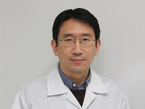
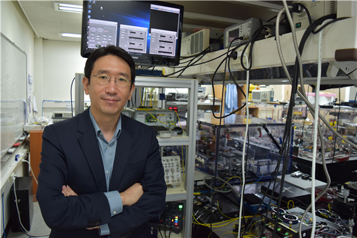 Scientist of October: Professor Jungwon Kim
Professor Jungwon Kim from the Department of Mechanical Engineering was selected as the ‘Scientist of the Month’ for October 2020 by the Ministry of Science and ICT and the National Research Foundation of Korea. Professor Kim was recognized for his contributions to expanding the horizons of the basics of precision engineering through his research on multifunctional ultrahigh-speed, high-resolution sensors. He received 10 million KRW in prize money.
Professor Kim was selected as the recipient of this award in celebration of “Measurement Day”, which commemorates October 26 as the day in which King Sejong the Great established a volume measurement system.
Professor Kim discovered that the time difference between the pulse of light created by a laser and the pulse of the current produced by a light-emitting diode was as small as 100 attoseconds (10-16 seconds). He then developed a unique multifunctional ultrahigh-speed, high-resolution Time-of-Flight (TOF) sensor that could take measurements of multiple points at the same time by sampling electric light. The sensor, with a measurement speed of 100 megahertz (100 million vibrations per second), a resolution of 180 picometers (1/5.5 billion meters), and a dynamic range of 150 decibels, overcame the limitations of both existing TOF techniques and laser interferometric techniques at the same time. The results of this research were published in Nature Photonics on February 10, 2020.
Professor Kim said, “I’d like to thank the graduate students who worked passionately with me, and KAIST for providing an environment in which I could fully focus on research. I am looking forward to the new and diverse applications in the field of machine manufacturing, such as studying the dynamic phenomena in microdevices, or taking ultraprecision measurement of shapes for advanced manufacturing.”
(END)
2020.10.15 View 13756
Scientist of October: Professor Jungwon Kim
Professor Jungwon Kim from the Department of Mechanical Engineering was selected as the ‘Scientist of the Month’ for October 2020 by the Ministry of Science and ICT and the National Research Foundation of Korea. Professor Kim was recognized for his contributions to expanding the horizons of the basics of precision engineering through his research on multifunctional ultrahigh-speed, high-resolution sensors. He received 10 million KRW in prize money.
Professor Kim was selected as the recipient of this award in celebration of “Measurement Day”, which commemorates October 26 as the day in which King Sejong the Great established a volume measurement system.
Professor Kim discovered that the time difference between the pulse of light created by a laser and the pulse of the current produced by a light-emitting diode was as small as 100 attoseconds (10-16 seconds). He then developed a unique multifunctional ultrahigh-speed, high-resolution Time-of-Flight (TOF) sensor that could take measurements of multiple points at the same time by sampling electric light. The sensor, with a measurement speed of 100 megahertz (100 million vibrations per second), a resolution of 180 picometers (1/5.5 billion meters), and a dynamic range of 150 decibels, overcame the limitations of both existing TOF techniques and laser interferometric techniques at the same time. The results of this research were published in Nature Photonics on February 10, 2020.
Professor Kim said, “I’d like to thank the graduate students who worked passionately with me, and KAIST for providing an environment in which I could fully focus on research. I am looking forward to the new and diverse applications in the field of machine manufacturing, such as studying the dynamic phenomena in microdevices, or taking ultraprecision measurement of shapes for advanced manufacturing.”
(END)
2020.10.15 View 13756 -
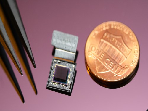 Ultrathin but Fully Packaged High-Resolution Camera
- Biologically inspired ultrathin arrayed camera captures super-resolution images. -
The unique structures of biological vision systems in nature inspired scientists to design ultracompact imaging systems. A research group led by Professor Ki-Hun Jeong have made an ultracompact camera that captures high-contrast and high-resolution images. Fully packaged with micro-optical elements such as inverted micro-lenses, multilayered pinhole arrays, and gap spacers on the image sensor, the camera boasts a total track length of 740 μm and a field of view of 73°.
Inspired by the eye structures of the paper wasp species Xenos peckii, the research team completely suppressed optical noise between micro-lenses while reducing camera thickness. The camera has successfully demonstrated high-contrast clear array images acquired from tiny micro lenses. To further enhance the image quality of the captured image, the team combined the arrayed images into one image through super-resolution imaging.
An insect’s compound eye has superior visual characteristics, such as a wide viewing angle, high motion sensitivity, and a large depth of field while maintaining a small volume of visual structure with a small focal length. Among them, the eyes of Xenos peckii and an endoparasite found on paper wasps have hundreds of photoreceptors in a single lens unlike conventional compound eyes. In particular, the eye structures of an adult Xenos peckii exhibit hundreds of photoreceptors on an individual eyelet and offer engineering inspiration for ultrathin cameras or imaging applications because they have higher visual acuity than other compound eyes.
For instance, Xenos peckii’s eye-inspired cameras provide a 50 times higher spatial resolution than those based on arthropod eyes. In addition, the effective image resolution of the Xenos peckii’s eye can be further improved using the image overlaps between neighboring eyelets. This unique structure offers higher visual resolution than other insect eyes.
The team achieved high-contrast and super-resolution imaging through a novel arrayed design of micro-optical elements comprising multilayered aperture arrays and inverted micro-lens arrays directly stacked over an image sensor. This optical component was integrated with a complementary metal oxide semiconductor image sensor.
This is first demonstration of super-resolution imaging which acquires a single integrated image with high contrast and high resolving power reconstructed from high-contrast array images. It is expected that this ultrathin arrayed camera can be applied for further developing mobile devices, advanced surveillance vehicles, and endoscopes.
Professor Jeong said, “This research has led to technological advances in imaging technology. We will continue to strive to make significant impacts on multidisciplinary research projects in the fields of microtechnology and nanotechnology, seeking inspiration from natural photonic structures.”
This work was featured in Light Science & Applications last month and was supported by the National Research Foundation (NRF) of and the Ministry of Health and Welfare (MOHW) of Korea.
Image credit: Professor Ki-Hun Jeong, KAIST
Image usage restrictions: News organizations may use or redistribute this image, with proper attribution, as part of news coverage of this paper only.
Publication:
Kisoo Kim, Kyung-Won Jang, Jae-Kwan Ryu, and Ki-Hun Jeong. (2020) “Biologically inspired ultrathin arrayed camera for high-contrast and high-resolution imaging”. Light Science & Applications. Volume 9. Article 28. Available online at https://doi.org/10.1038/s41377-020-0261-8
Profile:
Ki-Hun Jeong
Professor
kjeong@kaist.ac.kr
http://biophotonics.kaist.ac.kr/
Department of Bio and Brain Engineering
KAIST
Profile:
Kisoo Kim
Ph.D. Candidate
kisoo.kim1@kaist.ac.kr
http://biophotonics.kaist.ac.kr/
Department of Bio and Brain Engineering
KAIST
(END)
2020.03.23 View 20731
Ultrathin but Fully Packaged High-Resolution Camera
- Biologically inspired ultrathin arrayed camera captures super-resolution images. -
The unique structures of biological vision systems in nature inspired scientists to design ultracompact imaging systems. A research group led by Professor Ki-Hun Jeong have made an ultracompact camera that captures high-contrast and high-resolution images. Fully packaged with micro-optical elements such as inverted micro-lenses, multilayered pinhole arrays, and gap spacers on the image sensor, the camera boasts a total track length of 740 μm and a field of view of 73°.
Inspired by the eye structures of the paper wasp species Xenos peckii, the research team completely suppressed optical noise between micro-lenses while reducing camera thickness. The camera has successfully demonstrated high-contrast clear array images acquired from tiny micro lenses. To further enhance the image quality of the captured image, the team combined the arrayed images into one image through super-resolution imaging.
An insect’s compound eye has superior visual characteristics, such as a wide viewing angle, high motion sensitivity, and a large depth of field while maintaining a small volume of visual structure with a small focal length. Among them, the eyes of Xenos peckii and an endoparasite found on paper wasps have hundreds of photoreceptors in a single lens unlike conventional compound eyes. In particular, the eye structures of an adult Xenos peckii exhibit hundreds of photoreceptors on an individual eyelet and offer engineering inspiration for ultrathin cameras or imaging applications because they have higher visual acuity than other compound eyes.
For instance, Xenos peckii’s eye-inspired cameras provide a 50 times higher spatial resolution than those based on arthropod eyes. In addition, the effective image resolution of the Xenos peckii’s eye can be further improved using the image overlaps between neighboring eyelets. This unique structure offers higher visual resolution than other insect eyes.
The team achieved high-contrast and super-resolution imaging through a novel arrayed design of micro-optical elements comprising multilayered aperture arrays and inverted micro-lens arrays directly stacked over an image sensor. This optical component was integrated with a complementary metal oxide semiconductor image sensor.
This is first demonstration of super-resolution imaging which acquires a single integrated image with high contrast and high resolving power reconstructed from high-contrast array images. It is expected that this ultrathin arrayed camera can be applied for further developing mobile devices, advanced surveillance vehicles, and endoscopes.
Professor Jeong said, “This research has led to technological advances in imaging technology. We will continue to strive to make significant impacts on multidisciplinary research projects in the fields of microtechnology and nanotechnology, seeking inspiration from natural photonic structures.”
This work was featured in Light Science & Applications last month and was supported by the National Research Foundation (NRF) of and the Ministry of Health and Welfare (MOHW) of Korea.
Image credit: Professor Ki-Hun Jeong, KAIST
Image usage restrictions: News organizations may use or redistribute this image, with proper attribution, as part of news coverage of this paper only.
Publication:
Kisoo Kim, Kyung-Won Jang, Jae-Kwan Ryu, and Ki-Hun Jeong. (2020) “Biologically inspired ultrathin arrayed camera for high-contrast and high-resolution imaging”. Light Science & Applications. Volume 9. Article 28. Available online at https://doi.org/10.1038/s41377-020-0261-8
Profile:
Ki-Hun Jeong
Professor
kjeong@kaist.ac.kr
http://biophotonics.kaist.ac.kr/
Department of Bio and Brain Engineering
KAIST
Profile:
Kisoo Kim
Ph.D. Candidate
kisoo.kim1@kaist.ac.kr
http://biophotonics.kaist.ac.kr/
Department of Bio and Brain Engineering
KAIST
(END)
2020.03.23 View 20731 -
 Two More Cross-generation Collaborative Labs Open
< President Sung-Chul Shin (sixth from the left) and Professor Sun Chang Kim (seventh from the left) at the signboard ceremony of KAIST BioDesigneering Laboratory >
KAIST opened two more cross-generation collaborative labs last month. KAIST BioDesigneering Laboratory headed by Professor Sun Chang Kim from the Department of Biological Sciences and Nanophotonics Laboratory led by Professor Yong-Hee Lee from the Department of Physics have been selected to receive 500 million KRW funding for five years.
A four-member selection committee including the former President of ETH Zürich Professor Emeritus Ralph Eichler and Professor Kwang-Soo Kim of Harvard Medical School conducted a three-month review and evaluation for this selection to be made. With these two new labs onboard, a total of six cross-generation collaborative labs will be operated on campus.
The operation of cross-generation collaborative labs has been in trial since March last year, as one of the KAIST’s Vision 2031 research innovation initiatives. This novel approach is to pair up senior and junior faculty members for sustaining research and academic achievements even after the senior researcher retires, so that the spectrum of knowledge and research competitiveness can be extended to future generations. The selected labs will be funded for five years, and the funding will be extended if necessary. KAIST will continue to select new labs every year.
One of this year’s selectees Professor Sun Chang Kim will be teamed up with Professor Byung-Kwan Cho from the same department and Professor Jung Kyoon Choi from the Department of Bio and Brain Engineering to collaborate in the fields of synthetic biology, systems biology, and genetic engineering. This group mainly aims at designing and synthesizing optimal genomes that can efficiently manufacture protein drug and biomedical active materials. They will also strive to secure large amounts of high-functioning natural active substances, new adhesive antibacterial peptides, and eco-friendly ecological restoration materials. It is expected that collaboration between these three multigenerational professors will help innovate their bio-convergence technology and further strengthen their international competitiveness in the global bio-market.
Another world-renowned scholar Professor Yong-Hee Lee of photonic crystal laser study will be joined by Professor Minkyo Seo from the same department and Professor Hansuek Lee from the Graduate School of Nanoscience and Technology. They will explore the extreme limits of light-material interaction based on optical micro/nano resonators, with the goal of developing future nonlinear optoelectronic and quantum optical devices. The knowledge and technology newly gained from the research are expected to provide an important platform for a diverse range of fields from quantum communications to biophysics.
(END)
2019.09.06 View 12094
Two More Cross-generation Collaborative Labs Open
< President Sung-Chul Shin (sixth from the left) and Professor Sun Chang Kim (seventh from the left) at the signboard ceremony of KAIST BioDesigneering Laboratory >
KAIST opened two more cross-generation collaborative labs last month. KAIST BioDesigneering Laboratory headed by Professor Sun Chang Kim from the Department of Biological Sciences and Nanophotonics Laboratory led by Professor Yong-Hee Lee from the Department of Physics have been selected to receive 500 million KRW funding for five years.
A four-member selection committee including the former President of ETH Zürich Professor Emeritus Ralph Eichler and Professor Kwang-Soo Kim of Harvard Medical School conducted a three-month review and evaluation for this selection to be made. With these two new labs onboard, a total of six cross-generation collaborative labs will be operated on campus.
The operation of cross-generation collaborative labs has been in trial since March last year, as one of the KAIST’s Vision 2031 research innovation initiatives. This novel approach is to pair up senior and junior faculty members for sustaining research and academic achievements even after the senior researcher retires, so that the spectrum of knowledge and research competitiveness can be extended to future generations. The selected labs will be funded for five years, and the funding will be extended if necessary. KAIST will continue to select new labs every year.
One of this year’s selectees Professor Sun Chang Kim will be teamed up with Professor Byung-Kwan Cho from the same department and Professor Jung Kyoon Choi from the Department of Bio and Brain Engineering to collaborate in the fields of synthetic biology, systems biology, and genetic engineering. This group mainly aims at designing and synthesizing optimal genomes that can efficiently manufacture protein drug and biomedical active materials. They will also strive to secure large amounts of high-functioning natural active substances, new adhesive antibacterial peptides, and eco-friendly ecological restoration materials. It is expected that collaboration between these three multigenerational professors will help innovate their bio-convergence technology and further strengthen their international competitiveness in the global bio-market.
Another world-renowned scholar Professor Yong-Hee Lee of photonic crystal laser study will be joined by Professor Minkyo Seo from the same department and Professor Hansuek Lee from the Graduate School of Nanoscience and Technology. They will explore the extreme limits of light-material interaction based on optical micro/nano resonators, with the goal of developing future nonlinear optoelectronic and quantum optical devices. The knowledge and technology newly gained from the research are expected to provide an important platform for a diverse range of fields from quantum communications to biophysics.
(END)
2019.09.06 View 12094 -
 Professor YongKeun Park Wins the 2018 Fumio Okano Award
(Professor Park)
Professor YongKeun Park from the Department of Physics won the 2018 Fumio Okano Award in recognition of his contributions to 3D display technology development during the annual conference of the International Society for Optics and Photonics (SPIE) held last month in Orlando, Florida in the US.
The Fumio Okano Best 3D Paper Prize is presented annually in memory of Dr. Fumio Okano, a pioneer and innovator of 3D displays who passed away in 2013, for his contributions to the field of 3D TVs and displays. The award is sponsored by NHK-ES.
Professor Park and his team are developing novel technology for measuring and visualizing 3D images by applying random light scattering. He has published numerous papers on 3D holographic camera technology and 3000x enhanced performance of 3D holographic displays in renowned international journals such as Nature Photonics, Nature Communications, and Science Advances. His technology has drawn international attention from renowned media outlets including Newsweek and Forbes.
He has established two startups to commercialize his technology. Tomocube specializes in 3D imaging microscopes using holotomographic technology and the company exports their products to several countries including the US and Japan. The.Wave.Talk is exploring technology for examining pre-existing bacteria anywhere and anytime.
Professor Park’s innovations have already been recognized in and out of KAIST. In February, he was selected as the KAISTian of the Year for his outstanding research, commercialization, and startups. He was also decorated with the National Science Award in April by the Ministry of Science and ICT and the Hong Jin-Ki Innovation Award later in May by the Yumin Cultural Foundation.
Professor Park said, “3D holography is emerging as a significant technology with growing potential and positive impacts on our daily lives. However, the current technology lags far behind the levels displayed in SF movies. We will do our utmost to reach this level with more commercialization."
2018.05.31 View 12839
Professor YongKeun Park Wins the 2018 Fumio Okano Award
(Professor Park)
Professor YongKeun Park from the Department of Physics won the 2018 Fumio Okano Award in recognition of his contributions to 3D display technology development during the annual conference of the International Society for Optics and Photonics (SPIE) held last month in Orlando, Florida in the US.
The Fumio Okano Best 3D Paper Prize is presented annually in memory of Dr. Fumio Okano, a pioneer and innovator of 3D displays who passed away in 2013, for his contributions to the field of 3D TVs and displays. The award is sponsored by NHK-ES.
Professor Park and his team are developing novel technology for measuring and visualizing 3D images by applying random light scattering. He has published numerous papers on 3D holographic camera technology and 3000x enhanced performance of 3D holographic displays in renowned international journals such as Nature Photonics, Nature Communications, and Science Advances. His technology has drawn international attention from renowned media outlets including Newsweek and Forbes.
He has established two startups to commercialize his technology. Tomocube specializes in 3D imaging microscopes using holotomographic technology and the company exports their products to several countries including the US and Japan. The.Wave.Talk is exploring technology for examining pre-existing bacteria anywhere and anytime.
Professor Park’s innovations have already been recognized in and out of KAIST. In February, he was selected as the KAISTian of the Year for his outstanding research, commercialization, and startups. He was also decorated with the National Science Award in April by the Ministry of Science and ICT and the Hong Jin-Ki Innovation Award later in May by the Yumin Cultural Foundation.
Professor Park said, “3D holography is emerging as a significant technology with growing potential and positive impacts on our daily lives. However, the current technology lags far behind the levels displayed in SF movies. We will do our utmost to reach this level with more commercialization."
2018.05.31 View 12839 -
 Seong-Tae Kim Wins Robert-Wagner All-Conference Best Paper Award
(Ph.D. candidate Seong-Tae Kim)
Ph.D. candidate Seong-Tae Kim from the School of Electrical Engineering won the Robert Wagner All-Conference Best Student Paper Award during the 2018 International Society for Optics and Photonics (SPIE) Medical Imaging Conference, which was held in Houston last month.
Kim, supervised by Professor Yong Man Ro, received the award for his paper in the category of computer-aided diagnosis. His paper, titled “ICADx: Interpretable Computer-Aided Diagnosis of Breast Masses”, was selected as the best paper out of 900 submissions. The conference selects the best paper in nine different categories. His research provides new insights on diagnostic technology to detect breast cancer powered by deep learning.
2018.03.15 View 12380
Seong-Tae Kim Wins Robert-Wagner All-Conference Best Paper Award
(Ph.D. candidate Seong-Tae Kim)
Ph.D. candidate Seong-Tae Kim from the School of Electrical Engineering won the Robert Wagner All-Conference Best Student Paper Award during the 2018 International Society for Optics and Photonics (SPIE) Medical Imaging Conference, which was held in Houston last month.
Kim, supervised by Professor Yong Man Ro, received the award for his paper in the category of computer-aided diagnosis. His paper, titled “ICADx: Interpretable Computer-Aided Diagnosis of Breast Masses”, was selected as the best paper out of 900 submissions. The conference selects the best paper in nine different categories. His research provides new insights on diagnostic technology to detect breast cancer powered by deep learning.
2018.03.15 View 12380 -
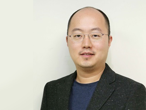
 Professor Jungwon Kim Wins Haerim Optics and Photonics Award
(Professor Jungwon Kim)
Professor Jungwon Kim from the Department of Mechanical Engineering received the 8th Haerim Optics and Photonics Award from the Optical Society of Korea (OSK).
He was recognized for his dedication to pioneering the field of microwave photonics by developing ultra-low noise fiber photonics lasers.
The Haerim Optics and Photonics Award is given to an outstanding researcher who has made academic contributions in the field of optics and photonics for the last five years.
The name of the award (Haerim) comes from the pen-name of the renowned scholar, Professor Un-Chul Paek, because it is maintained using funds he contributed to the OSK.
The OSK will confer the award on February 8 during the 29th OSK Annual Meeting and Winter Conference of 2018.
2018.02.07 View 9087
Professor Jungwon Kim Wins Haerim Optics and Photonics Award
(Professor Jungwon Kim)
Professor Jungwon Kim from the Department of Mechanical Engineering received the 8th Haerim Optics and Photonics Award from the Optical Society of Korea (OSK).
He was recognized for his dedication to pioneering the field of microwave photonics by developing ultra-low noise fiber photonics lasers.
The Haerim Optics and Photonics Award is given to an outstanding researcher who has made academic contributions in the field of optics and photonics for the last five years.
The name of the award (Haerim) comes from the pen-name of the renowned scholar, Professor Un-Chul Paek, because it is maintained using funds he contributed to the OSK.
The OSK will confer the award on February 8 during the 29th OSK Annual Meeting and Winter Conference of 2018.
2018.02.07 View 9087