%65%6d%69%73%73%69%6f%6e
-
 KAIST Develops OLED Technology with Double the Screen Brightness
<(From Left) Ph.D candidate Minjae Kim, Professor Seunghyup Yoo, Dr. Junho Kim>
Organic light-emitting diodes (OLEDs) are widely used in smartphones and TVs thanks to their excellent color reproduction and thin, flexible planar structure. However, internal light loss has limited further improvements in brightness. KAIST researchers have now developed a technology that more than doubles OLED light-emission efficiency while maintaining the flat structure that is a key advantage of OLED displays.
KAIST (President Kwang Hyung Lee) announced on the 11th of January that a research team led by Professor Seunghyup Yoo of the School of Electrical Engineering has developed a new near-planar light outcoupling structure* and an OLED design method that can significantly reduce light loss inside OLED devices.* Near-planar light outcoupling structure: a thin structure that keeps the OLED surface almost flat while extracting more of the light generated inside to the outside
OLEDs are composed of multiple layers of ultrathin organic films stacked on top of one another. As light passes through these layers, it is repeatedly reflected or absorbed, often causing more than 80% of the light generated inside the OLED to be lost as heat before it can escape.
To address this issue, light outcoupling structures such as hemispherical lenses or microlens arrays (MLAs) have been used to extract light from OLEDs. However, hemispherical lenses protrude significantly, making it difficult to maintain a flat form factor, while MLAs must cover much larger area than individual pixel sizes to achieve sufficient light extraction. This creates limitations in achieving high efficiency without interference between neighboring pixels.
To increase OLED brightness while preserving a planar structure, the research team proposed a new OLED design strategy that maximizes light extraction within the size of each individual pixel.
Unlike conventional designs that assume OLEDs extend infinitely, this approach takes into account the finite pixel sizes actually used in real displays. As a result, more light can be emitted externally even from pixels of the same size.
In addition, the team developed a new near-planar light outcoupling structure that helps light emerge efficiently in the forward direction without being spread too widely. This structure is very thin—comparable in thickness to existing microlens arrays—yet achieves light extraction efficiency close to that of hemispherical lenses of the same lateral dimension. As a result, it hardly undermines the flat form factors of OLEDs and can be readily applied to flexible OLED displays.
By combining the new OLED design with the near-planar light outcoupling structure, the researchers successfully achieved more than a twofold improvement in light-emission efficiency even in small pixels.
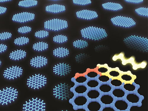
< Quasi-Planar Light Extraction OLED Technology >
This technology enables brighter displays using the same power while maintaining OLED’s flat structure, and is expected to extend battery life and reduce heat generation in mobile devices such as smartphones and tablets. Improvements in display lifespan are also anticipated.
MinJae Kim, the first author of the study, noted, “A small idea that came up during class was developed into real research results through the KAIST Undergraduate Research Program (URP).”
Professor Seunghyup Yoo stated, “Although many light outcoupling structures have been proposed, most were designed for large-area lighting applications, and many were difficult to apply effectively to displays composed of numerous small pixels,” adding, “The near-planar light outcoupling structure proposed in this work was designed with constraints on the size of the light source within each pixel, reducing optical interference between adjacent pixels while maximizing efficiency.” He further emphasized that the approach can be applied not only to OLEDs but also to next-generation display technologies based on materials such as perovskites and quantum dots.
< Schematic Overview and Application Examples of the Proposed Light Extraction Structure >
This research, with MinJae Kim (Department of Materials Science and Engineering, KAIST; currently a Ph.D. student in Materials Science and Engineering at Stanford University) and Junho Kim (School of Electrical Engineering, KAIST; currently a postdoctoral researcher at the University of Cologne, Germany) as co–first authors, was published online on December 29, 2025, in Nature Communications.
※ Paper title: “Near-planar light outcoupling structures with finite lateral dimensions for ultra-efficient and optical crosstalk-free OLED displays” DOI: 10.1038/s41467-025-66538-6
This research was supported by the KAIST Undergraduate Research Program (URP), the Mid-Career Researcher Program and the Future Display Strategic Research Lab Program of the National Research Foundation (NRF) of Korea, the Human Resource Development Program of the Korea Institute for Advancement of Technology (KIAT), and the Korea Planning & Evaluation Institute of Industrial Technology (KEIT).
2026.01.12 View 2517
KAIST Develops OLED Technology with Double the Screen Brightness
<(From Left) Ph.D candidate Minjae Kim, Professor Seunghyup Yoo, Dr. Junho Kim>
Organic light-emitting diodes (OLEDs) are widely used in smartphones and TVs thanks to their excellent color reproduction and thin, flexible planar structure. However, internal light loss has limited further improvements in brightness. KAIST researchers have now developed a technology that more than doubles OLED light-emission efficiency while maintaining the flat structure that is a key advantage of OLED displays.
KAIST (President Kwang Hyung Lee) announced on the 11th of January that a research team led by Professor Seunghyup Yoo of the School of Electrical Engineering has developed a new near-planar light outcoupling structure* and an OLED design method that can significantly reduce light loss inside OLED devices.* Near-planar light outcoupling structure: a thin structure that keeps the OLED surface almost flat while extracting more of the light generated inside to the outside
OLEDs are composed of multiple layers of ultrathin organic films stacked on top of one another. As light passes through these layers, it is repeatedly reflected or absorbed, often causing more than 80% of the light generated inside the OLED to be lost as heat before it can escape.
To address this issue, light outcoupling structures such as hemispherical lenses or microlens arrays (MLAs) have been used to extract light from OLEDs. However, hemispherical lenses protrude significantly, making it difficult to maintain a flat form factor, while MLAs must cover much larger area than individual pixel sizes to achieve sufficient light extraction. This creates limitations in achieving high efficiency without interference between neighboring pixels.
To increase OLED brightness while preserving a planar structure, the research team proposed a new OLED design strategy that maximizes light extraction within the size of each individual pixel.
Unlike conventional designs that assume OLEDs extend infinitely, this approach takes into account the finite pixel sizes actually used in real displays. As a result, more light can be emitted externally even from pixels of the same size.
In addition, the team developed a new near-planar light outcoupling structure that helps light emerge efficiently in the forward direction without being spread too widely. This structure is very thin—comparable in thickness to existing microlens arrays—yet achieves light extraction efficiency close to that of hemispherical lenses of the same lateral dimension. As a result, it hardly undermines the flat form factors of OLEDs and can be readily applied to flexible OLED displays.
By combining the new OLED design with the near-planar light outcoupling structure, the researchers successfully achieved more than a twofold improvement in light-emission efficiency even in small pixels.
< Quasi-Planar Light Extraction OLED Technology >
This technology enables brighter displays using the same power while maintaining OLED’s flat structure, and is expected to extend battery life and reduce heat generation in mobile devices such as smartphones and tablets. Improvements in display lifespan are also anticipated.
MinJae Kim, the first author of the study, noted, “A small idea that came up during class was developed into real research results through the KAIST Undergraduate Research Program (URP).”
Professor Seunghyup Yoo stated, “Although many light outcoupling structures have been proposed, most were designed for large-area lighting applications, and many were difficult to apply effectively to displays composed of numerous small pixels,” adding, “The near-planar light outcoupling structure proposed in this work was designed with constraints on the size of the light source within each pixel, reducing optical interference between adjacent pixels while maximizing efficiency.” He further emphasized that the approach can be applied not only to OLEDs but also to next-generation display technologies based on materials such as perovskites and quantum dots.
< Schematic Overview and Application Examples of the Proposed Light Extraction Structure >
This research, with MinJae Kim (Department of Materials Science and Engineering, KAIST; currently a Ph.D. student in Materials Science and Engineering at Stanford University) and Junho Kim (School of Electrical Engineering, KAIST; currently a postdoctoral researcher at the University of Cologne, Germany) as co–first authors, was published online on December 29, 2025, in Nature Communications.
※ Paper title: “Near-planar light outcoupling structures with finite lateral dimensions for ultra-efficient and optical crosstalk-free OLED displays” DOI: 10.1038/s41467-025-66538-6
This research was supported by the KAIST Undergraduate Research Program (URP), the Mid-Career Researcher Program and the Future Display Strategic Research Lab Program of the National Research Foundation (NRF) of Korea, the Human Resource Development Program of the Korea Institute for Advancement of Technology (KIAT), and the Korea Planning & Evaluation Institute of Industrial Technology (KEIT).
2026.01.12 View 2517 -
 First Elucidation of Spontaneous Emission and Excitation in Photonic Time Crystals
< (From left) Professor Bumki Min, Ph.D. Candidate Kyungmin Lee >
A groundbreaking discovery reveals that spontaneous emission, a key phenomenon in the interaction between light and atoms, manifests in a new form within a Photonic Time Crystal (PTC). This research, led by a KAIST team, not only overturns existing theory but further predicts a novel phenomenon: spontaneous emission excitation.
Professor Bumki Min's research team from the KAIST Department of Physics, in collaboration with Professor Jonghwa Shin of the Department of Materials Science and Engineering, Professor Wonju Jeon of the Department of Mechanical Engineering, Professor Gil Young Cho of the Department of Physics, and researchers from IBS, UC Berkeley, and the Hong Kong University of Science and Technology, announced that they have proven that the spontaneous emission decay rate in a Photonic Time Crystal is, on the contrary, enhanced rather than being "extinguished," as suggested by a paper published in Science in 2022. Furthermore, they predicted a new process—spontaneous emission excitation—where an atom transitions from its ground state to an excited state while simultaneously emitting a photon.
< Spontaneous emission decay rate (left) and spontaneous emission excitation rate (right) when a quantum emitter (or atom) is placed in an environment that changes very rapidly and periodically in time >
Spontaneous emission is the process by which an atom intrinsically emits a photon and is fundamental to quantum optics and photonic device research. Until now, control over spontaneous emission has been achieved by designing spatial structures like resonators or photonic crystals. However, the advent of Photonic Time Crystals, which periodically modulate the refractive index of a medium over time, has drawn attention to the potential for control along the time axis.
Previous theory predicted that the spontaneous emission decay rate in a Photonic Time Crystal would completely vanish at a specific frequency. In contrast, this study is the first to prove that the decay rate is significantly enhanced. This is attributed to the non-orthogonal mode effect, highlighting the importance of research into non-Hermitian optics.
The research team also predicted and reported a new process, 'spontaneous emission excitation,' where an atom gains energy and transitions from its ground state to an excited state while simultaneously emitting a photon. This is a non-equilibrium process made possible by the time-crystal medium supplying external energy, representing a new light-matter interaction phenomenon that cannot be explained by conventional equilibrium optics.
The findings fundamentally shift the paradigm of spontaneous emission research and hold promise for broad applications in fields such as quantum light source design and non-equilibrium quantum optics.
Professor Bumki Min stated, "This achievement re-establishes the fundamental theory describing spontaneous emission in a rapidly time-varying environment. The enhancement of spontaneous emission decay and the 'spontaneous emission excitation' phenomenon have the potential to change the paradigm of light-matter interaction research."
Ph.D. candidate Kyungmin Lee participated as the first author of this research. The results were published online in the international academic journal Physical Review Letters on September 23, 2025, simultaneously highlighted on Physics.org, and selected as an Editors' Suggestion paper. The research was supported by the National Research Foundation of Korea and the Samsung Science and Technology Foundation.
Note: The paper is titled “Spontaneous emission decay and excitation in photonic time crystals.”
2025.10.01 View 2652
First Elucidation of Spontaneous Emission and Excitation in Photonic Time Crystals
< (From left) Professor Bumki Min, Ph.D. Candidate Kyungmin Lee >
A groundbreaking discovery reveals that spontaneous emission, a key phenomenon in the interaction between light and atoms, manifests in a new form within a Photonic Time Crystal (PTC). This research, led by a KAIST team, not only overturns existing theory but further predicts a novel phenomenon: spontaneous emission excitation.
Professor Bumki Min's research team from the KAIST Department of Physics, in collaboration with Professor Jonghwa Shin of the Department of Materials Science and Engineering, Professor Wonju Jeon of the Department of Mechanical Engineering, Professor Gil Young Cho of the Department of Physics, and researchers from IBS, UC Berkeley, and the Hong Kong University of Science and Technology, announced that they have proven that the spontaneous emission decay rate in a Photonic Time Crystal is, on the contrary, enhanced rather than being "extinguished," as suggested by a paper published in Science in 2022. Furthermore, they predicted a new process—spontaneous emission excitation—where an atom transitions from its ground state to an excited state while simultaneously emitting a photon.
< Spontaneous emission decay rate (left) and spontaneous emission excitation rate (right) when a quantum emitter (or atom) is placed in an environment that changes very rapidly and periodically in time >
Spontaneous emission is the process by which an atom intrinsically emits a photon and is fundamental to quantum optics and photonic device research. Until now, control over spontaneous emission has been achieved by designing spatial structures like resonators or photonic crystals. However, the advent of Photonic Time Crystals, which periodically modulate the refractive index of a medium over time, has drawn attention to the potential for control along the time axis.
Previous theory predicted that the spontaneous emission decay rate in a Photonic Time Crystal would completely vanish at a specific frequency. In contrast, this study is the first to prove that the decay rate is significantly enhanced. This is attributed to the non-orthogonal mode effect, highlighting the importance of research into non-Hermitian optics.
The research team also predicted and reported a new process, 'spontaneous emission excitation,' where an atom gains energy and transitions from its ground state to an excited state while simultaneously emitting a photon. This is a non-equilibrium process made possible by the time-crystal medium supplying external energy, representing a new light-matter interaction phenomenon that cannot be explained by conventional equilibrium optics.
The findings fundamentally shift the paradigm of spontaneous emission research and hold promise for broad applications in fields such as quantum light source design and non-equilibrium quantum optics.
Professor Bumki Min stated, "This achievement re-establishes the fundamental theory describing spontaneous emission in a rapidly time-varying environment. The enhancement of spontaneous emission decay and the 'spontaneous emission excitation' phenomenon have the potential to change the paradigm of light-matter interaction research."
Ph.D. candidate Kyungmin Lee participated as the first author of this research. The results were published online in the international academic journal Physical Review Letters on September 23, 2025, simultaneously highlighted on Physics.org, and selected as an Editors' Suggestion paper. The research was supported by the National Research Foundation of Korea and the Samsung Science and Technology Foundation.
Note: The paper is titled “Spontaneous emission decay and excitation in photonic time crystals.”
2025.10.01 View 2652 -
 A New Strategy for the Optimal Electroreduction of CO2 to High-Value Products
-Researchers suggest that modulation of local CO2 concentration improves the selectivity, conversion rate, and electrode stability, and shed a new light on the electrochemical CO2 reduction technology for controlling emissions at a low cost.-
A KAIST research team presented three novel approaches for modulating local carbon dioxide (CO2) concentration in gas-diffusion electrode (GDE)-based flow electrolyzers. Their study also empirically demonstrated that providing a moderate local CO2 concentration is effective in promoting Carbon–Carbon (C–C) coupling reactions toward the production of multi-carbon molecules. This work, featured in the May 20th issue of Joule, serves as a rational guide to tune CO2 mass transport for the optimal production of valuable multi-carbon products.
Amid global efforts to reduce and recycle anthropogenic CO2 emissions, CO2 electrolysis holds great promise for converting CO2 into useful chemicals that were traditionally derived from fossil fuels. Many researches have been attempting to improve the selectivity of CO2 for commercially and industrially high-value multi-carbon products such as ethylene, ethanol, and 1-propanol, due to their high energy density and large market size.
In order to achieve the highly-selective conversion of CO2 into valuable multi-carbon products, past studies have focused on the design of catalysts and the tuning of local environment related to pH, cations, and molecular additives.
Conventional CO2 electrolytic systems relied heavily on an alkaline electrolyte that is often consumed in large quantities when reacting with CO2, and thus led to an increase in the operational costs. Moreover, the life span of a catalyst electrode was short, due to its inherent chemical reactivity.
In their recent study, a group of KAIST researchers led by Professor Jihun Oh from the Department of Materials Science and Engineering reported that the local CO2 concentration has been an overlooked factor that largely affects the selectivity toward multi-carbon products.
Professor Oh and his researchers Dr. Ying Chuan Tan, Hakhyeon Song, and Kelvin Berm Lee proposed that there is an intimate relation between local CO2 and multi-carbon product selectivity during electrochemical CO2 reduction reactions. The team employed the mass-transport modeling of a GDE-based flow electrolyzer that utilizes copper oxide (Cu2O) nanoparticles as model catalysts. They then identified and applied three approaches to modulate the local CO2 concentration within a GDE-based electrolytic system, including 1) controlling the catalyst layer structure, 2) CO2 feed concentration, and 3) feed flow rate.
Contrary to common intuition, the study showed that providing a maximum CO2 transport leads to suboptimal multi-carbon product faradaic efficiency. Instead, by restricting and providing a moderate local CO2 concentration, C–C coupling can be significantly enhanced.
The researchers demonstrated experimentally that the selectivity rate increased from 25.4% to 61.9%, and from 5.9% to 22.6% for the CO2 conversion rate. When a cheap milder near-neutral electrolyte was used, the stability of the CO2 electrolytic system improved to a great extent, allowing over 10 hours of steady selective production of multi-carbon products.
Dr. Tan, the lead author of the paper, said, “Our research clearly revealed that the optimization of the local CO2 concentration is the key to maximizing the efficiency of converting CO2 into high-value multi-carbon products.”
Professor Oh added, “This finding is expected to deliver new insights to the research community that variables affecting local CO2 concentration are also influential factors in the electrochemical CO2 reduction reaction performance. My colleagues and I hope that our study becomes a cornerstone for related technologies and their industrial applications.”
This work was supported by the Korean Ministry of Science and ICT (MSIT) Creative Materials Discovery Program.
Publication:
Tan, Y. C et al. (2020) ‘Modulating Local CO2 Concentration as a General Strategy for Enhancing C−C Coupling in CO2 Electroreduction’, Joule, Vol. 4, Issue 5, pp. 1104-1120. Available online at https://doi.org/10.1016/j.joule.2020.03.013
Profile: Jihun Oh, PhD
Associate Professor
jihun.oh@kaist.ac.kr
http://les.kaist.ac.kr/
Laboratory for Energy and Sustainability (LE&S)
Department of Materials Science and Engineering (MSE)
Korea Advanced Institute of Science and Technology (KAIST)
https://www.kaist.ac.kr
Daejeon 34141, Republic of Korea
Profile: Ying Chuan Tan, PhD
tanyc@kaist.ac.kr
LE&S, MSE, KAIST
Profile: Hakhyeon Song, PhD Candidate
hyeon0401@kaist.ac.kr
LE&S, MSE, KAIST
Profile: Kelvin Berm Lee, M.S. Candidate
kbl9105@kaist.ac.kr
LE&S, MSE, KAIST
(END)
2020.06.03 View 16506
A New Strategy for the Optimal Electroreduction of CO2 to High-Value Products
-Researchers suggest that modulation of local CO2 concentration improves the selectivity, conversion rate, and electrode stability, and shed a new light on the electrochemical CO2 reduction technology for controlling emissions at a low cost.-
A KAIST research team presented three novel approaches for modulating local carbon dioxide (CO2) concentration in gas-diffusion electrode (GDE)-based flow electrolyzers. Their study also empirically demonstrated that providing a moderate local CO2 concentration is effective in promoting Carbon–Carbon (C–C) coupling reactions toward the production of multi-carbon molecules. This work, featured in the May 20th issue of Joule, serves as a rational guide to tune CO2 mass transport for the optimal production of valuable multi-carbon products.
Amid global efforts to reduce and recycle anthropogenic CO2 emissions, CO2 electrolysis holds great promise for converting CO2 into useful chemicals that were traditionally derived from fossil fuels. Many researches have been attempting to improve the selectivity of CO2 for commercially and industrially high-value multi-carbon products such as ethylene, ethanol, and 1-propanol, due to their high energy density and large market size.
In order to achieve the highly-selective conversion of CO2 into valuable multi-carbon products, past studies have focused on the design of catalysts and the tuning of local environment related to pH, cations, and molecular additives.
Conventional CO2 electrolytic systems relied heavily on an alkaline electrolyte that is often consumed in large quantities when reacting with CO2, and thus led to an increase in the operational costs. Moreover, the life span of a catalyst electrode was short, due to its inherent chemical reactivity.
In their recent study, a group of KAIST researchers led by Professor Jihun Oh from the Department of Materials Science and Engineering reported that the local CO2 concentration has been an overlooked factor that largely affects the selectivity toward multi-carbon products.
Professor Oh and his researchers Dr. Ying Chuan Tan, Hakhyeon Song, and Kelvin Berm Lee proposed that there is an intimate relation between local CO2 and multi-carbon product selectivity during electrochemical CO2 reduction reactions. The team employed the mass-transport modeling of a GDE-based flow electrolyzer that utilizes copper oxide (Cu2O) nanoparticles as model catalysts. They then identified and applied three approaches to modulate the local CO2 concentration within a GDE-based electrolytic system, including 1) controlling the catalyst layer structure, 2) CO2 feed concentration, and 3) feed flow rate.
Contrary to common intuition, the study showed that providing a maximum CO2 transport leads to suboptimal multi-carbon product faradaic efficiency. Instead, by restricting and providing a moderate local CO2 concentration, C–C coupling can be significantly enhanced.
The researchers demonstrated experimentally that the selectivity rate increased from 25.4% to 61.9%, and from 5.9% to 22.6% for the CO2 conversion rate. When a cheap milder near-neutral electrolyte was used, the stability of the CO2 electrolytic system improved to a great extent, allowing over 10 hours of steady selective production of multi-carbon products.
Dr. Tan, the lead author of the paper, said, “Our research clearly revealed that the optimization of the local CO2 concentration is the key to maximizing the efficiency of converting CO2 into high-value multi-carbon products.”
Professor Oh added, “This finding is expected to deliver new insights to the research community that variables affecting local CO2 concentration are also influential factors in the electrochemical CO2 reduction reaction performance. My colleagues and I hope that our study becomes a cornerstone for related technologies and their industrial applications.”
This work was supported by the Korean Ministry of Science and ICT (MSIT) Creative Materials Discovery Program.
Publication:
Tan, Y. C et al. (2020) ‘Modulating Local CO2 Concentration as a General Strategy for Enhancing C−C Coupling in CO2 Electroreduction’, Joule, Vol. 4, Issue 5, pp. 1104-1120. Available online at https://doi.org/10.1016/j.joule.2020.03.013
Profile: Jihun Oh, PhD
Associate Professor
jihun.oh@kaist.ac.kr
http://les.kaist.ac.kr/
Laboratory for Energy and Sustainability (LE&S)
Department of Materials Science and Engineering (MSE)
Korea Advanced Institute of Science and Technology (KAIST)
https://www.kaist.ac.kr
Daejeon 34141, Republic of Korea
Profile: Ying Chuan Tan, PhD
tanyc@kaist.ac.kr
LE&S, MSE, KAIST
Profile: Hakhyeon Song, PhD Candidate
hyeon0401@kaist.ac.kr
LE&S, MSE, KAIST
Profile: Kelvin Berm Lee, M.S. Candidate
kbl9105@kaist.ac.kr
LE&S, MSE, KAIST
(END)
2020.06.03 View 16506 -
 Synthesizing Single-Crystalline Hexagonal Graphene Quantum Dots
(Figure: Uniformly ordered single-crystalline graphene quantum dots of various sizes synthesized through solution chemistry.)
A KAIST team has designed a novel strategy for synthesizing single-crystalline graphene quantum dots, which emit stable blue light. The research team confirmed that a display made of their synthesized graphene quantum dots successfully emitted blue light with stable electric pressure, reportedly resolving the long-standing challenges of blue light emission in manufactured displays. The study, led by Professor O Ok Park in the Department of Chemical and Biological Engineering, was featured online in Nano Letters on July 5.
Graphene has gained increased attention as a next-generation material for its heat and electrical conductivity as well as its transparency. However, single and multi-layered graphene have characteristics of a conductor so that it is difficult to apply into semiconductor. Only when downsized to the nanoscale, semiconductor’s distinct feature of bandgap will be exhibited to emit the light in the graphene. This illuminating featuring of dot is referred to as a graphene quantum dot.
Conventionally, single-crystalline graphene has been fabricated by chemical vapor deposition (CVD) on copper or nickel thin films, or by peeling graphite physically and chemically. However, graphene made via chemical vapor deposition is mainly used for large-surface transparent electrodes. Meanwhile, graphene made by chemical and physical peeling carries uneven size defects.
The research team explained that their graphene quantum dots exhibited a very stable single-phase reaction when they mixed amine and acetic acid with an aqueous solution of glucose. Then, they synthesized single-crystalline graphene quantum dots from the self-assembly of the reaction intermediate. In the course of fabrication, the team developed a new separation method at a low-temperature precipitation, which led to successfully creating a homogeneous nucleation of graphene quantum dots via a single-phase reaction.
Professor Park and his colleagues have developed solution phase synthesis technology that allows for the creation of the desired crystal size for single nanocrystals down to 100 nano meters. It is reportedly the first synthesis of the homogeneous nucleation of graphene through a single-phase reaction.
Professor Park said, "This solution method will significantly contribute to the grafting of graphene in various fields. The application of this new graphene will expand the scope of its applications such as for flexible displays and varistors.”
This research was a joint project with a team from Korea University under Professor Sang Hyuk Im from the Department of Chemical and Biological Engineering, and was supported by the National Research Foundation of Korea, the Nano-Material Technology Development Program from the Electronics and Telecommunications Research Institute (ETRI), KAIST EEWS, and the BK21+ project from the Korean government.
2019.08.02 View 41801
Synthesizing Single-Crystalline Hexagonal Graphene Quantum Dots
(Figure: Uniformly ordered single-crystalline graphene quantum dots of various sizes synthesized through solution chemistry.)
A KAIST team has designed a novel strategy for synthesizing single-crystalline graphene quantum dots, which emit stable blue light. The research team confirmed that a display made of their synthesized graphene quantum dots successfully emitted blue light with stable electric pressure, reportedly resolving the long-standing challenges of blue light emission in manufactured displays. The study, led by Professor O Ok Park in the Department of Chemical and Biological Engineering, was featured online in Nano Letters on July 5.
Graphene has gained increased attention as a next-generation material for its heat and electrical conductivity as well as its transparency. However, single and multi-layered graphene have characteristics of a conductor so that it is difficult to apply into semiconductor. Only when downsized to the nanoscale, semiconductor’s distinct feature of bandgap will be exhibited to emit the light in the graphene. This illuminating featuring of dot is referred to as a graphene quantum dot.
Conventionally, single-crystalline graphene has been fabricated by chemical vapor deposition (CVD) on copper or nickel thin films, or by peeling graphite physically and chemically. However, graphene made via chemical vapor deposition is mainly used for large-surface transparent electrodes. Meanwhile, graphene made by chemical and physical peeling carries uneven size defects.
The research team explained that their graphene quantum dots exhibited a very stable single-phase reaction when they mixed amine and acetic acid with an aqueous solution of glucose. Then, they synthesized single-crystalline graphene quantum dots from the self-assembly of the reaction intermediate. In the course of fabrication, the team developed a new separation method at a low-temperature precipitation, which led to successfully creating a homogeneous nucleation of graphene quantum dots via a single-phase reaction.
Professor Park and his colleagues have developed solution phase synthesis technology that allows for the creation of the desired crystal size for single nanocrystals down to 100 nano meters. It is reportedly the first synthesis of the homogeneous nucleation of graphene through a single-phase reaction.
Professor Park said, "This solution method will significantly contribute to the grafting of graphene in various fields. The application of this new graphene will expand the scope of its applications such as for flexible displays and varistors.”
This research was a joint project with a team from Korea University under Professor Sang Hyuk Im from the Department of Chemical and Biological Engineering, and was supported by the National Research Foundation of Korea, the Nano-Material Technology Development Program from the Electronics and Telecommunications Research Institute (ETRI), KAIST EEWS, and the BK21+ project from the Korean government.
2019.08.02 View 41801 -
 The key to Alzheimer disease, PET-MRI made in Korea
Professor Kyu-Sung Cho
- Simultaneous PET-MRI imaging system commercialization technology developed purely from domestic technology - - Inspiring achievement by KAIST, National NanoFab Center, Sogang University, Seoul National University Hospital –
Hopes are high for the potential of producing domestic products in the field of state-of-the-art medical imaging equipment that used to rely on imported products.
The joint research team (KAIST, Sogang University and Seoul National University) with KAIST Department of Nuclear and Quantum Engineering Professor Kyu-Sung Cho in charge, together with National Nanofab Institution (NNFC; Director Jae-Young Lee), has developed PET-MRI simultaneous imaging system with domestic technology only. The team successfully acquired brain images of 3 volunteers with the newly developed system.
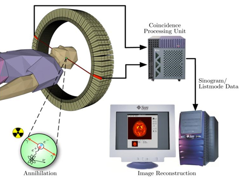
PET-MRI is integrated state-of-the-art medical imaging equipment that combines the advantages of Magnetic Resonance Imaging (MRI) that shows anatomical images of the body and Position Emission Tomography (PET) that analyses cell activity and metabolism. Since the anatomical information and functional information can be seen simultaneously, the device can be used to diagnose early onset Alzheimer’s disease and is essential in biological science research, such as new medicine development.
The existing equipment used to take MRI and PET images separately due to the strong magnetic field generated by MRI and combine the images. Hence, it was time consuming and error-prone due to patient’s movement. There was a need to develop PET that functions within a magnetic field to create a simultaneous imaging system.
The newly developed integral PET-MRI has 3 technical characteristics: 1. PET detector without magnetic interference, 2. PET-MRI integration system, 3.PET-MRI imaging processing.
The PET detector is the most important factor and accounts for half the cost of the whole system. KAIST Professor Cho and NNFC Doctor Woo-Suk Seol’s team successfully developed the Silicon Photomultiplier (amplifies light coming into the radiation detector) that can be used in strong magnetic fields. The developed sensor has a global competitive edge since it optimises semiconductor processing to yield over 95% productivity and around 10% gamma radiation energy resolving power.
Sogang University Department and Electrical Engineering Professor Yong Choi developed cutting edge PET system using a new concept of electric charge signal transmission method and imaging location distinction circuit. The creativity and excellence of the research findings were recognised and hence published on the cover of Medical Physics in June.
Seoul National University Hospital Department of Nuclear Medicine Professor Jae-Sung Lee developed the Silicon Photomultiplier sensor based PET imaging reconstitution programme, MRI imaging based PET imaging revision technology and PET-MRI imaging integration software.
Furthermore, KAIST Department of Electrical Engineering Professor Hyun-Wook Park was responsible for the development of RF Shielding technology that enables simultaneous installation of PET and MRI and using this technology, he developed a head coil for the brain that can be connected to PET for installation.
Based on the technology describe above, the joint research team successfully developed PET-MRI system for brains and acquired PET-MRI integrated brain images from 3 volunteers last June.
In particular, this system has the distinct feature of a detachable PET module and MRI head coil to the existing whole body MRI, so that PET-MRI simultaneous imaging is possible with low installation cost.
Professor Cho said, “We have prepared the foundation of domestic commercial PET and the system has a competitive edge in the global market of PET-MRI system technology.” He continued, “It can reduce the cost of the increasing brain related disease diagnosis, including Alzheimer’s, dramatically.”
Funded by Ministry of Trade, Industry and Energy as an Industrial Foundation Technology Development Project (98 billion won in 7 years), the research applied for over 20 patents and 20 CSI theses.
Figure 1.Brain phantom images from developed PET-MRI system
Figure 2. Brain images from developed PET-MRI system
Figure 3. Domestic PET-MRI clinical trial
Figure 4. Head RF coil and PET detector inserted in MRI
Figure 5. Insertion type PET detector module
Figure 6. Silicon Photomultiplier sensor (Left) and flash crystal block (right)
Figure7. Silicon Photomultiplier sensor
Figure 8. PET detection principle
2013.11.28 View 19157
The key to Alzheimer disease, PET-MRI made in Korea
Professor Kyu-Sung Cho
- Simultaneous PET-MRI imaging system commercialization technology developed purely from domestic technology - - Inspiring achievement by KAIST, National NanoFab Center, Sogang University, Seoul National University Hospital –
Hopes are high for the potential of producing domestic products in the field of state-of-the-art medical imaging equipment that used to rely on imported products.
The joint research team (KAIST, Sogang University and Seoul National University) with KAIST Department of Nuclear and Quantum Engineering Professor Kyu-Sung Cho in charge, together with National Nanofab Institution (NNFC; Director Jae-Young Lee), has developed PET-MRI simultaneous imaging system with domestic technology only. The team successfully acquired brain images of 3 volunteers with the newly developed system.
PET-MRI is integrated state-of-the-art medical imaging equipment that combines the advantages of Magnetic Resonance Imaging (MRI) that shows anatomical images of the body and Position Emission Tomography (PET) that analyses cell activity and metabolism. Since the anatomical information and functional information can be seen simultaneously, the device can be used to diagnose early onset Alzheimer’s disease and is essential in biological science research, such as new medicine development.
The existing equipment used to take MRI and PET images separately due to the strong magnetic field generated by MRI and combine the images. Hence, it was time consuming and error-prone due to patient’s movement. There was a need to develop PET that functions within a magnetic field to create a simultaneous imaging system.
The newly developed integral PET-MRI has 3 technical characteristics: 1. PET detector without magnetic interference, 2. PET-MRI integration system, 3.PET-MRI imaging processing.
The PET detector is the most important factor and accounts for half the cost of the whole system. KAIST Professor Cho and NNFC Doctor Woo-Suk Seol’s team successfully developed the Silicon Photomultiplier (amplifies light coming into the radiation detector) that can be used in strong magnetic fields. The developed sensor has a global competitive edge since it optimises semiconductor processing to yield over 95% productivity and around 10% gamma radiation energy resolving power.
Sogang University Department and Electrical Engineering Professor Yong Choi developed cutting edge PET system using a new concept of electric charge signal transmission method and imaging location distinction circuit. The creativity and excellence of the research findings were recognised and hence published on the cover of Medical Physics in June.
Seoul National University Hospital Department of Nuclear Medicine Professor Jae-Sung Lee developed the Silicon Photomultiplier sensor based PET imaging reconstitution programme, MRI imaging based PET imaging revision technology and PET-MRI imaging integration software.
Furthermore, KAIST Department of Electrical Engineering Professor Hyun-Wook Park was responsible for the development of RF Shielding technology that enables simultaneous installation of PET and MRI and using this technology, he developed a head coil for the brain that can be connected to PET for installation.
Based on the technology describe above, the joint research team successfully developed PET-MRI system for brains and acquired PET-MRI integrated brain images from 3 volunteers last June.
In particular, this system has the distinct feature of a detachable PET module and MRI head coil to the existing whole body MRI, so that PET-MRI simultaneous imaging is possible with low installation cost.
Professor Cho said, “We have prepared the foundation of domestic commercial PET and the system has a competitive edge in the global market of PET-MRI system technology.” He continued, “It can reduce the cost of the increasing brain related disease diagnosis, including Alzheimer’s, dramatically.”
Funded by Ministry of Trade, Industry and Energy as an Industrial Foundation Technology Development Project (98 billion won in 7 years), the research applied for over 20 patents and 20 CSI theses.
Figure 1.Brain phantom images from developed PET-MRI system
Figure 2. Brain images from developed PET-MRI system
Figure 3. Domestic PET-MRI clinical trial
Figure 4. Head RF coil and PET detector inserted in MRI
Figure 5. Insertion type PET detector module
Figure 6. Silicon Photomultiplier sensor (Left) and flash crystal block (right)
Figure7. Silicon Photomultiplier sensor
Figure 8. PET detection principle
2013.11.28 View 19157 -
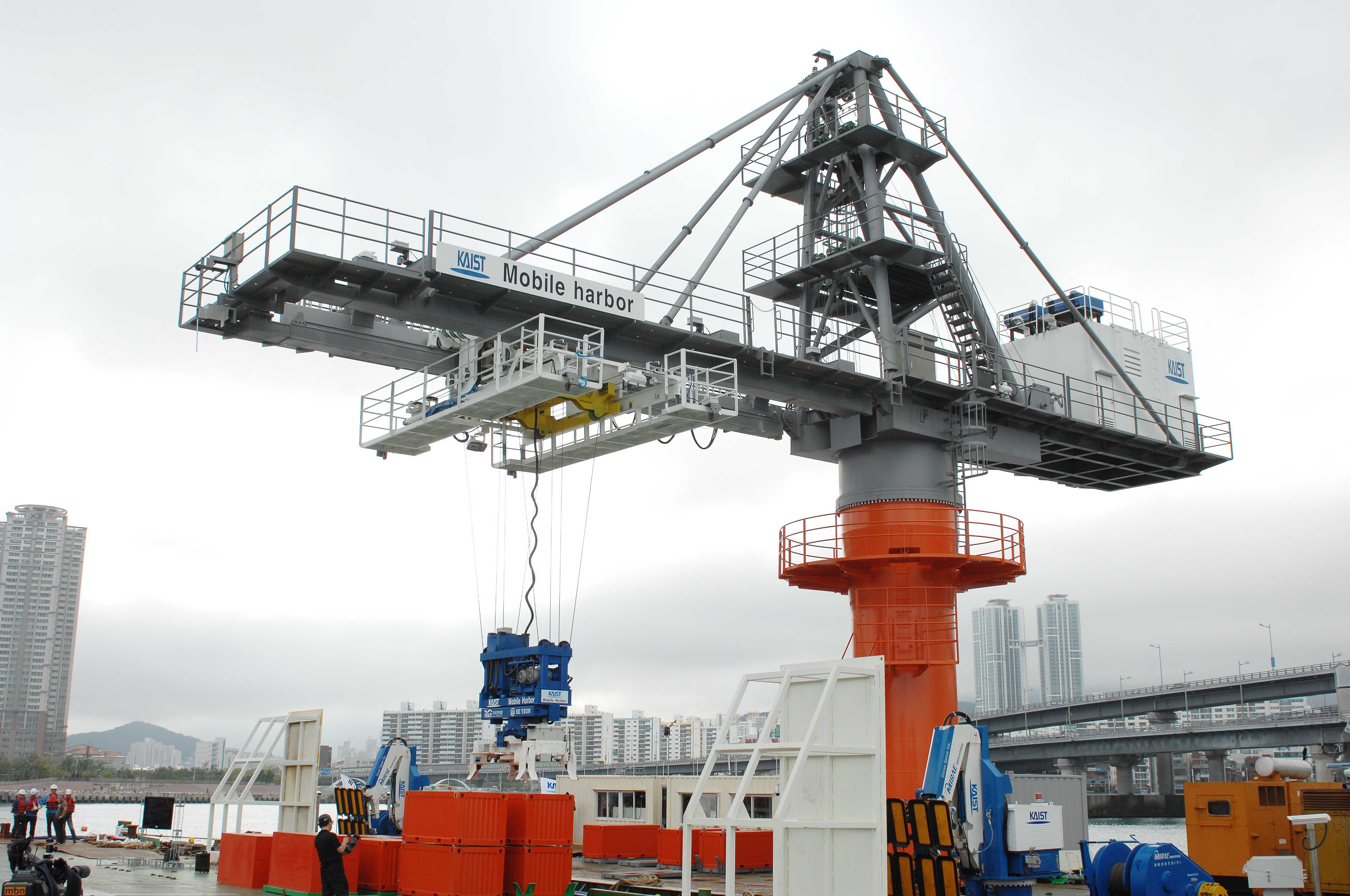 KAIST Successfully Demonstrates Mobile Harbor in the Open Sea
Busan, South Korea—Large container ships are no longer required to come into ports to transport cargo, as KAIST has developed an innovative technology that will transform the paradigm of today’s cargo handling operations. A Mobile Harbor is a vessel that carries a large stabilized crane with a smart spreader and multistage trolley system, enabling the loading and unloading of ship cargo on the wavy open sea. Following a successful docking of two vessels at sea in April of this year, KAIST conducted a full scope of Mobile Harbor operations in the inner sea of Busan, South Korea, on June 29, 2011.
Initiated in 2009, the Mobile Harbor (MH) is one of the university’s flagship research projects, which aims to provide a new growth engine that will lead the Korean economy to the next level of advancement, and to develop green technology through multidisciplinary and convergence research. The idea of MH came to light when thinking outside the box (why can’t a harbor go out to meet a ship on voyage and retrieve goods instead of ships coming into the harbor?) to improve problems relating to the current maritime transport system, such as port congestion, environmental issues caused by heavy sea transport, increased demand for supersized container ships, and the need for port construction and expansion.
The essential technology to establish a Mobile Harbor is a docking system and crane system that can overcome the obstacles imposed by the sea, i.e., waves and wind. Connecting two operating vessels of different sizes in the unpredictable and ever-changing environment of the sea was regarded as “impossible” and had never been tried before, but, on April 26, 2011, KAIST successfully demonstrated the technology to moor vessels safely and securely.
The Mobile Harbor has a unique way of mooring vessels that are anchored at sea: its flexibly designed robot arms with a square-shape vacuum suction pad at the tip reach out and attach to the hull of a container ship for docking. Each robot arm is connected to a cable and winch that further add stability to the Mobile Harbor. Foam-filled fenders are placed between the Mobile Harbor and the container ship, thereby maintaining a safe distance to prevent collisions.
The crane system consists of a multistage trolley, smart spreader, and tension controller, all of which provide the crane with functionality and stability to move around cargo containers in the sea. The crane system also has various sensors like cameras and laser scanners, and therefore, it can gauge the movement of the spreader and ships as well as trace a target container in real time. As a result, the spreader, a container grabbing device, is free from the swing motions when lifting and putting down cargo and grabs a target container safely in the wavy open sea.
During today’s at-sea demonstration in Busan, a research team from the KAIST Mobile Harbor Center docked a Mobile Harbor (a barge ship) right next to a container vessel (the other barge ship) and repeated freight transport operations between the two ships, presenting the great potential to commercialize the Mobile Harbor technology.
The project has been implemented in collaboration with industries, research institutes, and universities in such fields as mechanical engineering, robotics, automation engineering, and ocean systems engineering. The demonstration proceeded with a wide range of participants including researchers, engineers, government officials, and entrepreneurs from Korea and around the world.
Byung-Man Kwak, Director of the KAIST Mobile Harbor Center, explained his feelings on the successful demonstration:
“It’s been a remarkable journey to develop a Mobile Harbor from scratch, and I’m genuinely thrilled to showcase what we have accomplished so far. Today’s demonstration of Mobile Harbor’s core technologies will really change the face of our maritime transportation system. We will be able to deliver more goods to global markets and consumers via sea route, not necessarily building more ports or expanding the existing harbors. KAIST’s Mobile Harbor will also significantly cut down the high cost related to overland transportation of cargo and in return, contribute to the reduction of carbon emission.”
The Center has received much interest in possible market migration and broader application of the Mobile Harbor from businesses and organizations, e.g., US Office of Naval Research, King Fahd University of Petroleum and Minerals, Saudi Aramco, POSCO, and the Korean Navy.
2011.07.06 View 21817
KAIST Successfully Demonstrates Mobile Harbor in the Open Sea
Busan, South Korea—Large container ships are no longer required to come into ports to transport cargo, as KAIST has developed an innovative technology that will transform the paradigm of today’s cargo handling operations. A Mobile Harbor is a vessel that carries a large stabilized crane with a smart spreader and multistage trolley system, enabling the loading and unloading of ship cargo on the wavy open sea. Following a successful docking of two vessels at sea in April of this year, KAIST conducted a full scope of Mobile Harbor operations in the inner sea of Busan, South Korea, on June 29, 2011.
Initiated in 2009, the Mobile Harbor (MH) is one of the university’s flagship research projects, which aims to provide a new growth engine that will lead the Korean economy to the next level of advancement, and to develop green technology through multidisciplinary and convergence research. The idea of MH came to light when thinking outside the box (why can’t a harbor go out to meet a ship on voyage and retrieve goods instead of ships coming into the harbor?) to improve problems relating to the current maritime transport system, such as port congestion, environmental issues caused by heavy sea transport, increased demand for supersized container ships, and the need for port construction and expansion.
The essential technology to establish a Mobile Harbor is a docking system and crane system that can overcome the obstacles imposed by the sea, i.e., waves and wind. Connecting two operating vessels of different sizes in the unpredictable and ever-changing environment of the sea was regarded as “impossible” and had never been tried before, but, on April 26, 2011, KAIST successfully demonstrated the technology to moor vessels safely and securely.
The Mobile Harbor has a unique way of mooring vessels that are anchored at sea: its flexibly designed robot arms with a square-shape vacuum suction pad at the tip reach out and attach to the hull of a container ship for docking. Each robot arm is connected to a cable and winch that further add stability to the Mobile Harbor. Foam-filled fenders are placed between the Mobile Harbor and the container ship, thereby maintaining a safe distance to prevent collisions.
The crane system consists of a multistage trolley, smart spreader, and tension controller, all of which provide the crane with functionality and stability to move around cargo containers in the sea. The crane system also has various sensors like cameras and laser scanners, and therefore, it can gauge the movement of the spreader and ships as well as trace a target container in real time. As a result, the spreader, a container grabbing device, is free from the swing motions when lifting and putting down cargo and grabs a target container safely in the wavy open sea.
During today’s at-sea demonstration in Busan, a research team from the KAIST Mobile Harbor Center docked a Mobile Harbor (a barge ship) right next to a container vessel (the other barge ship) and repeated freight transport operations between the two ships, presenting the great potential to commercialize the Mobile Harbor technology.
The project has been implemented in collaboration with industries, research institutes, and universities in such fields as mechanical engineering, robotics, automation engineering, and ocean systems engineering. The demonstration proceeded with a wide range of participants including researchers, engineers, government officials, and entrepreneurs from Korea and around the world.
Byung-Man Kwak, Director of the KAIST Mobile Harbor Center, explained his feelings on the successful demonstration:
“It’s been a remarkable journey to develop a Mobile Harbor from scratch, and I’m genuinely thrilled to showcase what we have accomplished so far. Today’s demonstration of Mobile Harbor’s core technologies will really change the face of our maritime transportation system. We will be able to deliver more goods to global markets and consumers via sea route, not necessarily building more ports or expanding the existing harbors. KAIST’s Mobile Harbor will also significantly cut down the high cost related to overland transportation of cargo and in return, contribute to the reduction of carbon emission.”
The Center has received much interest in possible market migration and broader application of the Mobile Harbor from businesses and organizations, e.g., US Office of Naval Research, King Fahd University of Petroleum and Minerals, Saudi Aramco, POSCO, and the Korean Navy.
2011.07.06 View 21817 -
 Prof. Choi Unveils Method to Improve Emission Efficiency of OLED
A KAIST research team led by Prof. Kyung-Cheol Choi of the School of Electrical Engineering & Computer Science discovered the surface plasmon-enhanced spontaneous emission based on an organic light-emitting device (OLED), a finding expected to improve OLED"s emission efficiency, KAIST authorities said on Thursday (July 9).
For surface plasmon localization, silver nanoparticles were thermally deposited in a high vacuum on cathode. Since plasmons provide a strong oscillator decay channel, time-resolved photoluninescene (PL) results displayed a 1.75-fold increased emission rate, and continuous wave PL results showed a twofold enhanced intensity.
"The method using surface plasmon represents a new technology to enhance the emission efficiency of OLED. It is expected to greatly contribute to the development of new technologies in OLED and flexible display, as well as securing original technology," Prof. Choi said.
The finding was published in the April issue of Applied Physics Letters and the June 25 issue of Optics Express. It will be also featured as the research highlight of the August issue of Nature Photonics and Virtual Journal of Ultrafast Science.
2009.07.09 View 27831
Prof. Choi Unveils Method to Improve Emission Efficiency of OLED
A KAIST research team led by Prof. Kyung-Cheol Choi of the School of Electrical Engineering & Computer Science discovered the surface plasmon-enhanced spontaneous emission based on an organic light-emitting device (OLED), a finding expected to improve OLED"s emission efficiency, KAIST authorities said on Thursday (July 9).
For surface plasmon localization, silver nanoparticles were thermally deposited in a high vacuum on cathode. Since plasmons provide a strong oscillator decay channel, time-resolved photoluninescene (PL) results displayed a 1.75-fold increased emission rate, and continuous wave PL results showed a twofold enhanced intensity.
"The method using surface plasmon represents a new technology to enhance the emission efficiency of OLED. It is expected to greatly contribute to the development of new technologies in OLED and flexible display, as well as securing original technology," Prof. Choi said.
The finding was published in the April issue of Applied Physics Letters and the June 25 issue of Optics Express. It will be also featured as the research highlight of the August issue of Nature Photonics and Virtual Journal of Ultrafast Science.
2009.07.09 View 27831 -
 Yoonsun Doh Wins 'Outstanding Poster Paper Award' at IDW
Yoonsun Doh Wins ‘Outstanding Poster Paper Award’ at IDW
Yoonsun Doh, a master-course student at the Division of Electrical Engineering (Advisory professor Kyungchul Choi) won the Outstanding Poster Paper Award at IDW 2006, which was held at Otsu, Japan on December 8, 2006.
The title of Doh’s paper is ‘Relationship between IR Emission of Reset Discharge and Image Retention in AC PDP’.
At the paper, Doh proposed a method capable of quantitatively measuring the temporary image-sticking phenomena, which is raised as a problem that impairs the quality of images on an AC PDP.
2006.12.26 View 19607
Yoonsun Doh Wins 'Outstanding Poster Paper Award' at IDW
Yoonsun Doh Wins ‘Outstanding Poster Paper Award’ at IDW
Yoonsun Doh, a master-course student at the Division of Electrical Engineering (Advisory professor Kyungchul Choi) won the Outstanding Poster Paper Award at IDW 2006, which was held at Otsu, Japan on December 8, 2006.
The title of Doh’s paper is ‘Relationship between IR Emission of Reset Discharge and Image Retention in AC PDP’.
At the paper, Doh proposed a method capable of quantitatively measuring the temporary image-sticking phenomena, which is raised as a problem that impairs the quality of images on an AC PDP.
2006.12.26 View 19607