Wave
-
 KAIST and Mainz Researchers Unveil 3D Magnon Control, Charting a New Course for Neuromorphic and Quantum Technologies
< Professor Se Kwon Kim of the Department of Physics (left), Dr. Zarzuela of the University of Mainz, Germany (right) >
What if the magnon Hall effect, which processes information using magnons (spin waves) capable of current-free information transfer with magnets, could overcome its current limitation of being possible only on a 2D plane? If magnons could be utilized in 3D space, they would enable flexible design, including 3D circuits, and be applicable in various fields such as next-generation neuromorphic (brain-mimicking) computing structures, similar to human brain information processing. KAIST and an international joint research team have, for the first time in the world, predicted a 3D magnon Hall effect, demonstrating that magnons can move freely and complexly in 3D space, transcending the conventional concept of magnons.
KAIST (President Kwang Hyung Lee) announced on May 22nd that Professor Se Kwon Kim of the Department of Physics, in collaboration with Dr. Ricardo Zarzuela of the University of Mainz, Germany, has revealed that the interaction between magnons (spin waves) and solitons (spin vortices) within complex magnetic structures (topologically textured frustrated magnets) is not simple, but complex in a way that enables novel functionalities.
Magnons (spin waves), which can transmit information like electron movement, are garnering attention as a next-generation information processing technology that transmits information without using current, thus generating no heat. Until now, magnon research has focused on simple magnets where spins are neatly aligned in one direction, and the mathematics describing this was a relatively simple 'Abelian gauge theory.'
The research team demonstrated, for the first time in the world, that in complex spin structures like frustrated magnets, magnons interact and become entangled in complex ways from various directions. They applied an advanced mathematical framework, 'non-Abelian gauge theory,' to describe this movement, which is a groundbreaking achievement.
This research presents the possibility of future applications in low-power logic devices using magnons and topology-based quantum information processing technologies, indicating a potential paradigm shift in future information technology.
In conventional linear magnetic materials, the value representing the magnetic state (order parameter) is given as a vector. In magnonics research based on this, it has been interpreted that a U(1) Abelian gauge field is induced when magnons move in soliton structures like skyrmions. This means that the interaction between solitons and magnons has a structure similar to quantum electrodynamics (QED), which has successfully explained various experimental results such as the magnon Hall effect in 2D magnets.
< Figure. Schematic diagram of non-Abelian magnon quantum chromodynamics describing the dynamics of three types of magnons discovered for the first time in this study.>
However, through this research, the team theoretically revealed that in frustrated magnets, the order parameter must be expressed not as a simple vector but as a quaternion. As a result, the gauge field experienced by magnons resembles an SU(3) non-Abelian gauge field, rather than a simple U(1) Abelian gauge field.
This implies that within frustrated magnets, there are not one or two types of magnons seen in conventional magnets, but three distinct types of magnons, each interacting and intricately entangled with solitons. This structure is highly significant as it resembles quantum chromodynamics (QCD) that describes the strong interaction between quarks mediated by gluons rather than quantum electrodynamics (QED) that describes electromagnetic forces.
Professor Se Kwon Kim stated, "This research presents a powerful theoretical framework to explain the dynamics of magnons occurring within the complex order of frustrated magnets," adding, "By pioneering non-Abelian magnonics, it will be a conceptual turning point that can influence quantum magnetism research as a whole."
The research results, with Dr. Ricardo Zarzuela of the University of Mainz, Germany, as the first author, were published in the world-renowned physics journal Physical Review Letters on May 6th.※ Paper title: "Non-Abelian Gauge Theory for Magnons in Topologically Textured Frustrated Magnets," Phys. Rev. Lett. 134, 186701 (2025)DOI: https://doi.org/10.1103/PhysRevLett.134.186701
This research was supported by the Brain Pool Plus program of the National Research Foundation of Korea.
2025.05.22 View 501
KAIST and Mainz Researchers Unveil 3D Magnon Control, Charting a New Course for Neuromorphic and Quantum Technologies
< Professor Se Kwon Kim of the Department of Physics (left), Dr. Zarzuela of the University of Mainz, Germany (right) >
What if the magnon Hall effect, which processes information using magnons (spin waves) capable of current-free information transfer with magnets, could overcome its current limitation of being possible only on a 2D plane? If magnons could be utilized in 3D space, they would enable flexible design, including 3D circuits, and be applicable in various fields such as next-generation neuromorphic (brain-mimicking) computing structures, similar to human brain information processing. KAIST and an international joint research team have, for the first time in the world, predicted a 3D magnon Hall effect, demonstrating that magnons can move freely and complexly in 3D space, transcending the conventional concept of magnons.
KAIST (President Kwang Hyung Lee) announced on May 22nd that Professor Se Kwon Kim of the Department of Physics, in collaboration with Dr. Ricardo Zarzuela of the University of Mainz, Germany, has revealed that the interaction between magnons (spin waves) and solitons (spin vortices) within complex magnetic structures (topologically textured frustrated magnets) is not simple, but complex in a way that enables novel functionalities.
Magnons (spin waves), which can transmit information like electron movement, are garnering attention as a next-generation information processing technology that transmits information without using current, thus generating no heat. Until now, magnon research has focused on simple magnets where spins are neatly aligned in one direction, and the mathematics describing this was a relatively simple 'Abelian gauge theory.'
The research team demonstrated, for the first time in the world, that in complex spin structures like frustrated magnets, magnons interact and become entangled in complex ways from various directions. They applied an advanced mathematical framework, 'non-Abelian gauge theory,' to describe this movement, which is a groundbreaking achievement.
This research presents the possibility of future applications in low-power logic devices using magnons and topology-based quantum information processing technologies, indicating a potential paradigm shift in future information technology.
In conventional linear magnetic materials, the value representing the magnetic state (order parameter) is given as a vector. In magnonics research based on this, it has been interpreted that a U(1) Abelian gauge field is induced when magnons move in soliton structures like skyrmions. This means that the interaction between solitons and magnons has a structure similar to quantum electrodynamics (QED), which has successfully explained various experimental results such as the magnon Hall effect in 2D magnets.
< Figure. Schematic diagram of non-Abelian magnon quantum chromodynamics describing the dynamics of three types of magnons discovered for the first time in this study.>
However, through this research, the team theoretically revealed that in frustrated magnets, the order parameter must be expressed not as a simple vector but as a quaternion. As a result, the gauge field experienced by magnons resembles an SU(3) non-Abelian gauge field, rather than a simple U(1) Abelian gauge field.
This implies that within frustrated magnets, there are not one or two types of magnons seen in conventional magnets, but three distinct types of magnons, each interacting and intricately entangled with solitons. This structure is highly significant as it resembles quantum chromodynamics (QCD) that describes the strong interaction between quarks mediated by gluons rather than quantum electrodynamics (QED) that describes electromagnetic forces.
Professor Se Kwon Kim stated, "This research presents a powerful theoretical framework to explain the dynamics of magnons occurring within the complex order of frustrated magnets," adding, "By pioneering non-Abelian magnonics, it will be a conceptual turning point that can influence quantum magnetism research as a whole."
The research results, with Dr. Ricardo Zarzuela of the University of Mainz, Germany, as the first author, were published in the world-renowned physics journal Physical Review Letters on May 6th.※ Paper title: "Non-Abelian Gauge Theory for Magnons in Topologically Textured Frustrated Magnets," Phys. Rev. Lett. 134, 186701 (2025)DOI: https://doi.org/10.1103/PhysRevLett.134.186701
This research was supported by the Brain Pool Plus program of the National Research Foundation of Korea.
2025.05.22 View 501 -
 KAIST Innovates Mid-Infrared Photodetectors for Exoplanet Detection, Expanding Applications to Environmental and Medical Fields
NASA’s James Webb Space Telescope (JWST) utilizes mid-infrared spectroscopy to precisely analyze molecular components such as water vapor and sulfur dioxide in exoplanet atmospheres. The key to this analysis, where each molecule exhibits a unique spectral "fingerprint," lies in highly sensitive photodetector technology capable of measuring extremely weak light intensities. Recently, KAIST researchers have developed an innovative photodetector capable of detecting a broad range of mid-infrared spectra, garnering significant attention.
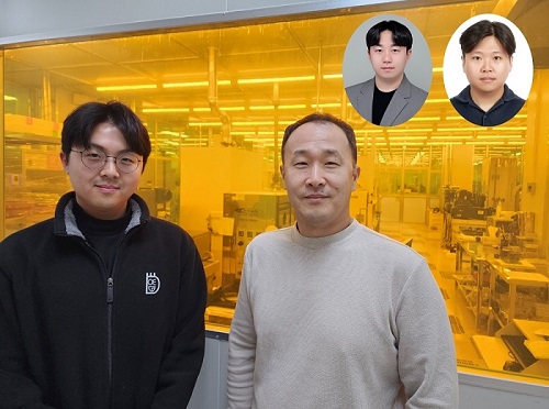
< Photo 1. (from the left) Ph.D. candidate Inki Kim (co-author), Professor SangHyeon Kim (corresponding author), Dr. Joonsup Shim (first author), and Dr. Jinha Lim (co-author) of KAIST School of Electrical Engineering. >
KAIST (represented by President Kwang-Hyung Lee) announced on the 27th of March that a research team led by Professor SangHyeon Kim from the School of Electrical Engineering has developed a mid-infrared photodetector that operates stably at room temperature, marking a major turning point for the commercialization of ultra-compact optical sensors.
The newly developed photodetector utilizes conventional silicon-based CMOS processes, enabling low-cost mass production while maintaining stable operation at room temperature. Notably, the research team successfully demonstrated the real-time detection of carbon dioxide (CO₂) gas using ultra-compact and ultra-thin optical sensors equipped with this photodetector, proving its potential for environmental monitoring and hazardous gas analysis.
Existing mid-infrared photodetectors generally require cooling systems due to high thermal noise at room temperature. These cooling systems increase the size and cost of equipment, making miniaturization and integration into portable devices challenging. Furthermore, conventional mid-infrared photodetectors are incompatible with silicon-based CMOS processes, limiting large-scale production and commercialization.
To address these limitations, the research team developed a waveguide-integrated photodetector using germanium (Ge), a Group IV element like silicon. This approach enables broad-spectrum mid-infrared detection while ensuring stable operation at room temperature.
< Figure 1. Schematic diagram of a room-temperature mid-infrared waveguide-integrated photodetector based on the Ge-on-insulator optical platform proposed in this study (top). Optical microscope image of the integrated photodetector connected with the sensing unit (bottom). >
A waveguide is a structure designed to efficiently guide light along a specific path with minimal loss. To implement various optical functions on a chip (on-chip), the development of waveguide-integrated photodetectors and waveguide-based optical components is essential.
Unlike conventional photodetectors that primarily rely on bandgap absorption principles, this new technology leverages the bolometric effect*, allowing it to detect the entire mid-infrared spectral range. As a result, it can be widely applied to the real-time sensing of various molecular species.
*Bolometric effect: A principle in which light absorption leads to an increase in temperature, causing electrical signals to change accordingly.
The waveguide-integrated mid-infrared photodetector developed by the research team is considered a groundbreaking innovation that overcomes the limitations of existing mid-infrared sensor technologies, including the need for cooling, difficulties in mass production, and high costs.
< Figure 2. Room temperature photoresponse characteristics of the mid-infrared waveguide photodetector proposed in this study (left) and real-time carbon dioxide (CO2) gas sensing results using the photodetector (right). >
This breakthrough technology is expected to be applicable across diverse fields, including environmental monitoring, medical diagnostics, industrial process management, national defense and security, and smart devices. It also paves the way for next-generation mid-infrared sensor advancements.
Professor SangHyeon Kim from KAIST stated, "This research represents a novel approach that overcomes the limitations of existing mid-infrared photodetector technologies and has great potential for practical applications in various fields." He further emphasized, "Since this sensor technology is compatible with CMOS processes, it enables low-cost mass production, making it highly suitable for next-generation environmental monitoring systems and smart manufacturing sites."
< Figure 3. Performance comparison image of a room-temperature mid-infrared waveguide photodetector fabricated with the technology proposed in this study. It achieves the world’s highest performance compared to existing technologies utilizing the Bolometric effect, and is the only solution compatible with CMOS processes. The technology proposed by our research team is characterized by its ability to respond to a wide spectrum of the mid-infrared band without limitations. >
The study, with Dr. Joonsup Shim (currently a postdoctoral researcher at Harvard University) as the first author, was published on March 19, 2025 in the internationally renowned journal Light: Science & Applications (JCR 2.9%, IF=20.6).
(Paper title: “Room-temperature waveguide-integrated photodetector using bolometric effect for mid-infrared spectroscopy applications,” https://doi.org/10.1038/s41377-025-01803-3)
2025.03.27 View 803
KAIST Innovates Mid-Infrared Photodetectors for Exoplanet Detection, Expanding Applications to Environmental and Medical Fields
NASA’s James Webb Space Telescope (JWST) utilizes mid-infrared spectroscopy to precisely analyze molecular components such as water vapor and sulfur dioxide in exoplanet atmospheres. The key to this analysis, where each molecule exhibits a unique spectral "fingerprint," lies in highly sensitive photodetector technology capable of measuring extremely weak light intensities. Recently, KAIST researchers have developed an innovative photodetector capable of detecting a broad range of mid-infrared spectra, garnering significant attention.
< Photo 1. (from the left) Ph.D. candidate Inki Kim (co-author), Professor SangHyeon Kim (corresponding author), Dr. Joonsup Shim (first author), and Dr. Jinha Lim (co-author) of KAIST School of Electrical Engineering. >
KAIST (represented by President Kwang-Hyung Lee) announced on the 27th of March that a research team led by Professor SangHyeon Kim from the School of Electrical Engineering has developed a mid-infrared photodetector that operates stably at room temperature, marking a major turning point for the commercialization of ultra-compact optical sensors.
The newly developed photodetector utilizes conventional silicon-based CMOS processes, enabling low-cost mass production while maintaining stable operation at room temperature. Notably, the research team successfully demonstrated the real-time detection of carbon dioxide (CO₂) gas using ultra-compact and ultra-thin optical sensors equipped with this photodetector, proving its potential for environmental monitoring and hazardous gas analysis.
Existing mid-infrared photodetectors generally require cooling systems due to high thermal noise at room temperature. These cooling systems increase the size and cost of equipment, making miniaturization and integration into portable devices challenging. Furthermore, conventional mid-infrared photodetectors are incompatible with silicon-based CMOS processes, limiting large-scale production and commercialization.
To address these limitations, the research team developed a waveguide-integrated photodetector using germanium (Ge), a Group IV element like silicon. This approach enables broad-spectrum mid-infrared detection while ensuring stable operation at room temperature.
< Figure 1. Schematic diagram of a room-temperature mid-infrared waveguide-integrated photodetector based on the Ge-on-insulator optical platform proposed in this study (top). Optical microscope image of the integrated photodetector connected with the sensing unit (bottom). >
A waveguide is a structure designed to efficiently guide light along a specific path with minimal loss. To implement various optical functions on a chip (on-chip), the development of waveguide-integrated photodetectors and waveguide-based optical components is essential.
Unlike conventional photodetectors that primarily rely on bandgap absorption principles, this new technology leverages the bolometric effect*, allowing it to detect the entire mid-infrared spectral range. As a result, it can be widely applied to the real-time sensing of various molecular species.
*Bolometric effect: A principle in which light absorption leads to an increase in temperature, causing electrical signals to change accordingly.
The waveguide-integrated mid-infrared photodetector developed by the research team is considered a groundbreaking innovation that overcomes the limitations of existing mid-infrared sensor technologies, including the need for cooling, difficulties in mass production, and high costs.
< Figure 2. Room temperature photoresponse characteristics of the mid-infrared waveguide photodetector proposed in this study (left) and real-time carbon dioxide (CO2) gas sensing results using the photodetector (right). >
This breakthrough technology is expected to be applicable across diverse fields, including environmental monitoring, medical diagnostics, industrial process management, national defense and security, and smart devices. It also paves the way for next-generation mid-infrared sensor advancements.
Professor SangHyeon Kim from KAIST stated, "This research represents a novel approach that overcomes the limitations of existing mid-infrared photodetector technologies and has great potential for practical applications in various fields." He further emphasized, "Since this sensor technology is compatible with CMOS processes, it enables low-cost mass production, making it highly suitable for next-generation environmental monitoring systems and smart manufacturing sites."
< Figure 3. Performance comparison image of a room-temperature mid-infrared waveguide photodetector fabricated with the technology proposed in this study. It achieves the world’s highest performance compared to existing technologies utilizing the Bolometric effect, and is the only solution compatible with CMOS processes. The technology proposed by our research team is characterized by its ability to respond to a wide spectrum of the mid-infrared band without limitations. >
The study, with Dr. Joonsup Shim (currently a postdoctoral researcher at Harvard University) as the first author, was published on March 19, 2025 in the internationally renowned journal Light: Science & Applications (JCR 2.9%, IF=20.6).
(Paper title: “Room-temperature waveguide-integrated photodetector using bolometric effect for mid-infrared spectroscopy applications,” https://doi.org/10.1038/s41377-025-01803-3)
2025.03.27 View 803 -
 KAIST Wins CES 2025 Innovation Award, Showcasing Innovative Technologies
KAIST will showcase innovative technologies at the world’s largest technology fair, the Consumer Electronics Show (CES 2025). In addition, KAIST startups VIRNECT Inc., Standard Energy Inc., A2US Inc., and Panmnesia, Inc. won the 2025 CES Innovation Awards.
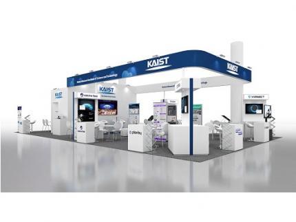
< Image 1. 3D-Graphical Profile of CES 2025 KAIST Exhibition Booth >
KAIST (President Kwang-Hyung Lee) announced on the 31st that it will operate a 140㎡ standalone booth at CES Eureka Park, which will be held in Las Vegas, USA from January 7th to 10th next year, to showcase KAIST's innovative technologies to global companies and investors.
KAIST startups VIRNECT, Standard Energy, A2US, and Panmnesia, Inc. won the 2025 CES Innovation Awards. ▴VIRNECT won the Innovation Award in the ‘Industrial Equipment and Machinery’ category for ‘VisionX’, an AI-based smart glass for industrial sites; ▴Standard Energy Co., Ltd. won the Innovation Award in the ‘Smart City’ category for developing the world’s first vanadium-ion battery; ▴A2US won the Innovation Award in the ‘Environment & Energy’ category for its portable air purifier that eliminates bacteria, odors, and fine dust in the air with just water droplets; ▴Panmnesia, Inc. won the Innovation Award in the ‘Computer Peripherals and Accessories’ category for its ‘CXL-based GPU Memory Expansion Kit’ that can drastically reduce the cost of building AI infrastructure.
< Image 2. (From left on the top row) VIRNECT, Standard Energy, (From left on the bottom row) A2US, Panmnesia, Inc. >
This exhibition will feature 15 startups that are standing out in cutting-edge technologies such as artificial intelligence (AI), robotics, mobility, and sustainability. In particular, AI-based deep tech startups in various industries such as logistics, architecture, and medicine will take up half of the total, showcasing the companies’ innovative AI technologies.
Polyphenol Factory Co.,Ltd introduces ‘Grabity’, a hair loss shampoo launched domestically, which applies the patented ingredient ‘LiftMax 308™’ that forms an instantaneous protective layer on the hair during the shampooing process. A real-time demonstration will be held at this exhibition hall so that visitors can experience the effects of the ingredient directly, and plans to enter the global market starting with the launch on Amazon in the US in January 2025.
VIRNECT will present ‘VisionX’, a prototype that won the Innovation Award this time. The product provides a chatbot AI through an AI voice interface, and has a function that allows users to check the status of the equipment in real time through conversations with the AI and receive troubleshooting guidance through voice conversations, so users can experience it directly at the KAIST Hall.
‘Standard Energy’ plans to exhibit ‘Energy Tile’, an indoor ESS that utilizes the world’s first vanadium ion battery (hereinafter referred to as VIB). VIB is absolutely safe from fire and has high installation flexibility, so it can be applied to smart cities and AI data centers.
‘A2US’ is the only company in the world that has hydroxyl radical water production technology, and won the Innovation Award for its first product, an air purifier. In the future, it is expected to be widely commercialized in air and water purification, smart farms, food tech, and semiconductor cleaning using safe and environmentally friendly hydroxyl radical water.
Panmnesia, Inc. won the CES Innovation Award for its GPU memory expansion solution equipped with its CXL 3.1 IP. By connecting a memory expansion device using Panmnesia’s CXL IP, the GPU’s memory capacity can be expanded to the terabyte level. Following the Innovation Award for ‘CXL-equipped AI Accelerator’ at CES 2024 last year, it is the only company to have won the Innovation Award for its AI-oriented CXL solution for two consecutive years.
In addition, technologies from a total of 15 companies will be introduced, including ▴Omelet ▴NEXTWAVE ▴Planby Technologies ▴Cosmo Bee ▴ImpactAI ▴Roen Surgical ▴DIDEN Roboticss ▴Autopedia ▴OAQ ▴HydroXpand ▴BOOKEND ▴Sterri.
On the central stage of the KAIST Hall, KAIST students selected as CES Student Supporters will conduct interviews with participating companies and promote the companies' innovative technologies and solutions. On the 8th, from 5 PM to 7 PM, a KAIST NIGHT event will be held where pre-invited investors and participating companies can network.
Keon Jae Lee, the head of the Institute of Technology Value Creation, said, “Through CES 2025, we will showcase innovative technologies and solutions from startups based on KAIST’s deep science and deep tech, and lead commercialization in cutting-edge technology fields such as AI, robotics, mobility, and environment/energy. KAIST plans to further promote technology commercialization by supporting the growth and marketing of innovative startups through the Institute of Technology Value Creation and by strengthening global networks and expanding cooperation opportunities.”
2024.12.31 View 4057
KAIST Wins CES 2025 Innovation Award, Showcasing Innovative Technologies
KAIST will showcase innovative technologies at the world’s largest technology fair, the Consumer Electronics Show (CES 2025). In addition, KAIST startups VIRNECT Inc., Standard Energy Inc., A2US Inc., and Panmnesia, Inc. won the 2025 CES Innovation Awards.
< Image 1. 3D-Graphical Profile of CES 2025 KAIST Exhibition Booth >
KAIST (President Kwang-Hyung Lee) announced on the 31st that it will operate a 140㎡ standalone booth at CES Eureka Park, which will be held in Las Vegas, USA from January 7th to 10th next year, to showcase KAIST's innovative technologies to global companies and investors.
KAIST startups VIRNECT, Standard Energy, A2US, and Panmnesia, Inc. won the 2025 CES Innovation Awards. ▴VIRNECT won the Innovation Award in the ‘Industrial Equipment and Machinery’ category for ‘VisionX’, an AI-based smart glass for industrial sites; ▴Standard Energy Co., Ltd. won the Innovation Award in the ‘Smart City’ category for developing the world’s first vanadium-ion battery; ▴A2US won the Innovation Award in the ‘Environment & Energy’ category for its portable air purifier that eliminates bacteria, odors, and fine dust in the air with just water droplets; ▴Panmnesia, Inc. won the Innovation Award in the ‘Computer Peripherals and Accessories’ category for its ‘CXL-based GPU Memory Expansion Kit’ that can drastically reduce the cost of building AI infrastructure.
< Image 2. (From left on the top row) VIRNECT, Standard Energy, (From left on the bottom row) A2US, Panmnesia, Inc. >
This exhibition will feature 15 startups that are standing out in cutting-edge technologies such as artificial intelligence (AI), robotics, mobility, and sustainability. In particular, AI-based deep tech startups in various industries such as logistics, architecture, and medicine will take up half of the total, showcasing the companies’ innovative AI technologies.
Polyphenol Factory Co.,Ltd introduces ‘Grabity’, a hair loss shampoo launched domestically, which applies the patented ingredient ‘LiftMax 308™’ that forms an instantaneous protective layer on the hair during the shampooing process. A real-time demonstration will be held at this exhibition hall so that visitors can experience the effects of the ingredient directly, and plans to enter the global market starting with the launch on Amazon in the US in January 2025.
VIRNECT will present ‘VisionX’, a prototype that won the Innovation Award this time. The product provides a chatbot AI through an AI voice interface, and has a function that allows users to check the status of the equipment in real time through conversations with the AI and receive troubleshooting guidance through voice conversations, so users can experience it directly at the KAIST Hall.
‘Standard Energy’ plans to exhibit ‘Energy Tile’, an indoor ESS that utilizes the world’s first vanadium ion battery (hereinafter referred to as VIB). VIB is absolutely safe from fire and has high installation flexibility, so it can be applied to smart cities and AI data centers.
‘A2US’ is the only company in the world that has hydroxyl radical water production technology, and won the Innovation Award for its first product, an air purifier. In the future, it is expected to be widely commercialized in air and water purification, smart farms, food tech, and semiconductor cleaning using safe and environmentally friendly hydroxyl radical water.
Panmnesia, Inc. won the CES Innovation Award for its GPU memory expansion solution equipped with its CXL 3.1 IP. By connecting a memory expansion device using Panmnesia’s CXL IP, the GPU’s memory capacity can be expanded to the terabyte level. Following the Innovation Award for ‘CXL-equipped AI Accelerator’ at CES 2024 last year, it is the only company to have won the Innovation Award for its AI-oriented CXL solution for two consecutive years.
In addition, technologies from a total of 15 companies will be introduced, including ▴Omelet ▴NEXTWAVE ▴Planby Technologies ▴Cosmo Bee ▴ImpactAI ▴Roen Surgical ▴DIDEN Roboticss ▴Autopedia ▴OAQ ▴HydroXpand ▴BOOKEND ▴Sterri.
On the central stage of the KAIST Hall, KAIST students selected as CES Student Supporters will conduct interviews with participating companies and promote the companies' innovative technologies and solutions. On the 8th, from 5 PM to 7 PM, a KAIST NIGHT event will be held where pre-invited investors and participating companies can network.
Keon Jae Lee, the head of the Institute of Technology Value Creation, said, “Through CES 2025, we will showcase innovative technologies and solutions from startups based on KAIST’s deep science and deep tech, and lead commercialization in cutting-edge technology fields such as AI, robotics, mobility, and environment/energy. KAIST plans to further promote technology commercialization by supporting the growth and marketing of innovative startups through the Institute of Technology Value Creation and by strengthening global networks and expanding cooperation opportunities.”
2024.12.31 View 4057 -
 KAIST Secures Core Technology for Ultra-High-Resolution Image Sensors
A joint research team from Korea and the United States has developed next-generation, high-resolution image sensor technology with higher power efficiency and a smaller size compared to existing sensors. Notably, they have secured foundational technology for ultra-high-resolution shortwave infrared (SWIR) image sensors, an area currently dominated by Sony, paving the way for future market entry.
KAIST (represented by President Kwang Hyung Lee) announced on the 20th of November that a research team led by Professor SangHyeon Kim from the School of Electrical Engineering, in collaboration with Inha University and Yale University in the U.S., has developed an ultra-thin broadband photodiode (PD), marking a significant breakthrough in high-performance image sensor technology.
This research drastically improves the trade-off between the absorption layer thickness and quantum efficiency found in conventional photodiode technology. Specifically, it achieved high quantum efficiency of over 70% even in an absorption layer thinner than one micrometer (μm), reducing the thickness of the absorption layer by approximately 70% compared to existing technologies.
A thinner absorption layer simplifies pixel processing, allowing for higher resolution and smoother carrier diffusion, which is advantageous for light carrier acquisition while also reducing the cost. However, a fundamental issue with thinner absorption layers is the reduced absorption of long-wavelength light.
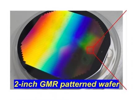
< Figure 1. Schematic diagram of the InGaAs photodiode image sensor integrated on the Guided-Mode Resonance (GMR) structure proposed in this study (left), a photograph of the fabricated wafer, and a scanning electron microscope (SEM) image of the periodic patterns (right) >
The research team introduced a guided-mode resonance (GMR) structure* that enables high-efficiency light absorption across a wide spectral range from 400 nanometers (nm) to 1,700 nanometers (nm). This wavelength range includes not only visible light but also light the SWIR region, making it valuable for various industrial applications.
*Guided-Mode Resonance (GMR) Structure: A concept used in electromagnetics, a phenomenon in which a specific (light) wave resonates (forming a strong electric/magnetic field) at a specific wavelength. Since energy is maximized under these conditions, it has been used to increase antenna or radar efficiency.
The improved performance in the SWIR region is expected to play a significant role in developing next-generation image sensors with increasingly high resolutions. The GMR structure, in particular, holds potential for further enhancing resolution and other performance metrics through hybrid integration and monolithic 3D integration with complementary metal-oxide-semiconductor (CMOS)-based readout integrated circuits (ROIC).
< Figure 2. Benchmark for state-of-the-art InGaAs-based SWIR pixels with simulated EQE lines as a function of TAL variation. Performance is maintained while reducing the absorption layer thickness from 2.1 micrometers or more to 1 micrometer or less while reducing it by 50% to 70% >
The research team has significantly enhanced international competitiveness in low-power devices and ultra-high-resolution imaging technology, opening up possibilities for applications in digital cameras, security systems, medical and industrial image sensors, as well as future ultra-high-resolution sensors for autonomous driving, aerospace, and satellite observation.
Professor Sang Hyun Kim, the lead researcher, commented, “This research demonstrates that significantly higher performance than existing technologies can be achieved even with ultra-thin absorption layers.”
< Figure 3. Top optical microscope image and cross-sectional scanning electron microscope image of the InGaAs photodiode image sensor fabricated on the GMR structure (left). Improved quantum efficiency performance of the ultra-thin image sensor (red) fabricated with the technology proposed in this study (right) >
The results of this research were published on 15th of November, in the prestigious international journal Light: Science & Applications (JCR 2.9%, IF=20.6), with Professor Dae-Myung Geum of Inha University (formerly a KAIST postdoctoral researcher) and Dr. Jinha Lim (currently a postdoctoral researcher at Yale University) as co-first authors. (Paper title: “Highly-efficient (>70%) and Wide-spectral (400 nm -1700 nm) sub-micron-thick InGaAs photodiodes for future high-resolution image sensors”)
This study was supported by the National Research Foundation of Korea.
2024.11.22 View 3709
KAIST Secures Core Technology for Ultra-High-Resolution Image Sensors
A joint research team from Korea and the United States has developed next-generation, high-resolution image sensor technology with higher power efficiency and a smaller size compared to existing sensors. Notably, they have secured foundational technology for ultra-high-resolution shortwave infrared (SWIR) image sensors, an area currently dominated by Sony, paving the way for future market entry.
KAIST (represented by President Kwang Hyung Lee) announced on the 20th of November that a research team led by Professor SangHyeon Kim from the School of Electrical Engineering, in collaboration with Inha University and Yale University in the U.S., has developed an ultra-thin broadband photodiode (PD), marking a significant breakthrough in high-performance image sensor technology.
This research drastically improves the trade-off between the absorption layer thickness and quantum efficiency found in conventional photodiode technology. Specifically, it achieved high quantum efficiency of over 70% even in an absorption layer thinner than one micrometer (μm), reducing the thickness of the absorption layer by approximately 70% compared to existing technologies.
A thinner absorption layer simplifies pixel processing, allowing for higher resolution and smoother carrier diffusion, which is advantageous for light carrier acquisition while also reducing the cost. However, a fundamental issue with thinner absorption layers is the reduced absorption of long-wavelength light.
< Figure 1. Schematic diagram of the InGaAs photodiode image sensor integrated on the Guided-Mode Resonance (GMR) structure proposed in this study (left), a photograph of the fabricated wafer, and a scanning electron microscope (SEM) image of the periodic patterns (right) >
The research team introduced a guided-mode resonance (GMR) structure* that enables high-efficiency light absorption across a wide spectral range from 400 nanometers (nm) to 1,700 nanometers (nm). This wavelength range includes not only visible light but also light the SWIR region, making it valuable for various industrial applications.
*Guided-Mode Resonance (GMR) Structure: A concept used in electromagnetics, a phenomenon in which a specific (light) wave resonates (forming a strong electric/magnetic field) at a specific wavelength. Since energy is maximized under these conditions, it has been used to increase antenna or radar efficiency.
The improved performance in the SWIR region is expected to play a significant role in developing next-generation image sensors with increasingly high resolutions. The GMR structure, in particular, holds potential for further enhancing resolution and other performance metrics through hybrid integration and monolithic 3D integration with complementary metal-oxide-semiconductor (CMOS)-based readout integrated circuits (ROIC).
< Figure 2. Benchmark for state-of-the-art InGaAs-based SWIR pixels with simulated EQE lines as a function of TAL variation. Performance is maintained while reducing the absorption layer thickness from 2.1 micrometers or more to 1 micrometer or less while reducing it by 50% to 70% >
The research team has significantly enhanced international competitiveness in low-power devices and ultra-high-resolution imaging technology, opening up possibilities for applications in digital cameras, security systems, medical and industrial image sensors, as well as future ultra-high-resolution sensors for autonomous driving, aerospace, and satellite observation.
Professor Sang Hyun Kim, the lead researcher, commented, “This research demonstrates that significantly higher performance than existing technologies can be achieved even with ultra-thin absorption layers.”
< Figure 3. Top optical microscope image and cross-sectional scanning electron microscope image of the InGaAs photodiode image sensor fabricated on the GMR structure (left). Improved quantum efficiency performance of the ultra-thin image sensor (red) fabricated with the technology proposed in this study (right) >
The results of this research were published on 15th of November, in the prestigious international journal Light: Science & Applications (JCR 2.9%, IF=20.6), with Professor Dae-Myung Geum of Inha University (formerly a KAIST postdoctoral researcher) and Dr. Jinha Lim (currently a postdoctoral researcher at Yale University) as co-first authors. (Paper title: “Highly-efficient (>70%) and Wide-spectral (400 nm -1700 nm) sub-micron-thick InGaAs photodiodes for future high-resolution image sensors”)
This study was supported by the National Research Foundation of Korea.
2024.11.22 View 3709 -
 KAIST holds its first ‘KAIST Tech Fair’ in New York, USA
< Photo 1. 2023 KAIST Tech Fair in New York >
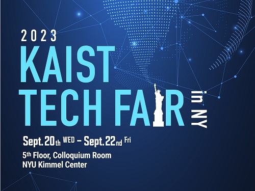
KAIST (President Kwang-Hyung Lee) announced on the 11th that it will hold the ‘2023 KAIST Tech Fair in New York’ at the Kimmel Center at New York University in Manhattan, USA, on the 22nd of this month. It is an event designed to be the starting point for KAIST to expand its startup ecosystem into the global stage, and it is to attract investments and secure global customers in New York by demonstrating the technological value of KAIST startup companies directly at location.
< Photo 2. President Kwang Hyung Lee at the 2023 KAIST Tech Fair in New York >
KAIST has been holding briefing sessions for technology transfer in Korea every year since 2018, and this year is the first time to hold a tech fair overseas for global companies.
KAIST Institute of Technology Value Creation (Director Sung-Yool Choi) has prepared for this event over the past six months with the Korea International Trade Association (hereinafter KITA, CEO Christopher Koo) to survey customer base and investment companies to conduct market analysis.
Among the companies founded with the technologies developed by the faculty and students of KAIST and their partners, 7 companies were selected to be matched with companies overseas that expressed interests in these technologies. Global multinational companies in the fields of IT, artificial intelligence, environment, logistics, distribution, and retail are participating as demand agencies and are testing the marketability of the start-up's technology as of September.
Daim Research, founded by Professor Young Jae Jang of the Department of Industrial and Systems Engineering, is a company specializing in smart factory automation solutions and is knocking on the door of the global market with a platform technology optimized for automated logistics systems.
< Photo 3. Presentation by Professor Young Jae Jang for DAIM Research >
It is a ‘collaborative intelligence’ solution that maximizes work productivity by having a number of robots used in industrial settings collaborate with one another. The strength of their solution is that logistics robots equipped with AI reinforced learning technology can respond to processes and environmental changes on their own, minimizing maintenance costs and the system can achieve excellent performance even with a small amount of data when it is combined with the digital twin technology the company has developed on its own.
A student startup, ‘Aniai’, is entering the US market, the home of hamburgers, with hamburger patty automation equipments and solutions. This is a robot kitchen startup founded by its CEO Gunpil Hwang, a graduate of KAIST’s School of Electrical Engineering which gathered together the experts in the fields of robot control, design, and artificial intelligence and cognitive technology to develop technology to automatically cook hamburger patties.
At the touch of a button, both sides of the patty are cooked simultaneously for consistent taste and quality according to the set condition. Since it can cook about 200 dishes in an hour, it is attracting attention as a technology that can not only solve manpower shortages but also accelerate the digital transformation of the restaurant industry.
Also, at the tech fair to be held at the Kimmel Center of New York University on the 22nd, the following startups who are currently under market verification in the U.S. will be participating: ▴'TheWaveTalk', which developed a water quality management system that can measure external substances and metal ions by transferring original technology from KAIST; ▴‘VIRNECT’, which helps workers improve their skills by remotely managing industrial sites using XR*; ▴‘Datumo’, a solution that helps process and analyze artificial intelligence big data, ▴‘VESSL AI’, the provider of a solution to eliminate the overhead** of machine learning systems; and ▴ ‘DolbomDream’, which developed an inflatable vest that helps the psychological stability of people with developmental disabilities.
* XR (eXtended Reality): Ultra-realistic technology that enhances immersion by utilizing augmented reality, virtual reality, and mixed reality technologies
** Overhead: Additional time required for stable processing of the program
In addition, two companies (Plasmapp and NotaAI) that are participating in the D-Unicorn program with the support of the Daejeon City and two companies (Enget and ILIAS Biologics) that are receiving support from the Scale Up Tips of the Ministry of SMEs and Startups, three companies (WiPowerOne, IDK Lab, and Artificial Photosynthesis Lab) that are continuing to realize the sustainable development goals for a total of 14 KAIST startups, will hold a corporate information session with about 100 invited guests from global companies and venture capital.
< Photo 4. Presentation for AP Lab >
Prior to this event, participating startups will be visiting the New York Economic Development Corporation and large law firms to receive advice on U.S. government support programs and on their attemps to enter the U.S. market. In addition, the participating companies plan to visit a startup support investment institution pursuing sustainable development goals and the Leslie eLab, New York University's one-stop startup support space, to lay the foundation for KAIST's leap forward in global technology commercialization.
< Photo 5. Sung-Yool Choi, the Director of KAIST Institute of Technology Value Creation (left) at the 2023 KAIST Tech Fair in New York with the key participants >
Sung-Yool Choi, the Director of KAIST Institute of Technology Value Creation, said, “KAIST prepared this event to realize its vision of being a leading university in creating global value.” He added, “We hope that our startups founded with KAIST technology would successfully completed market verification to be successful in securing global demands and in attracting investments for their endeavors.”
2023.09.11 View 15402
KAIST holds its first ‘KAIST Tech Fair’ in New York, USA
< Photo 1. 2023 KAIST Tech Fair in New York >
KAIST (President Kwang-Hyung Lee) announced on the 11th that it will hold the ‘2023 KAIST Tech Fair in New York’ at the Kimmel Center at New York University in Manhattan, USA, on the 22nd of this month. It is an event designed to be the starting point for KAIST to expand its startup ecosystem into the global stage, and it is to attract investments and secure global customers in New York by demonstrating the technological value of KAIST startup companies directly at location.
< Photo 2. President Kwang Hyung Lee at the 2023 KAIST Tech Fair in New York >
KAIST has been holding briefing sessions for technology transfer in Korea every year since 2018, and this year is the first time to hold a tech fair overseas for global companies.
KAIST Institute of Technology Value Creation (Director Sung-Yool Choi) has prepared for this event over the past six months with the Korea International Trade Association (hereinafter KITA, CEO Christopher Koo) to survey customer base and investment companies to conduct market analysis.
Among the companies founded with the technologies developed by the faculty and students of KAIST and their partners, 7 companies were selected to be matched with companies overseas that expressed interests in these technologies. Global multinational companies in the fields of IT, artificial intelligence, environment, logistics, distribution, and retail are participating as demand agencies and are testing the marketability of the start-up's technology as of September.
Daim Research, founded by Professor Young Jae Jang of the Department of Industrial and Systems Engineering, is a company specializing in smart factory automation solutions and is knocking on the door of the global market with a platform technology optimized for automated logistics systems.
< Photo 3. Presentation by Professor Young Jae Jang for DAIM Research >
It is a ‘collaborative intelligence’ solution that maximizes work productivity by having a number of robots used in industrial settings collaborate with one another. The strength of their solution is that logistics robots equipped with AI reinforced learning technology can respond to processes and environmental changes on their own, minimizing maintenance costs and the system can achieve excellent performance even with a small amount of data when it is combined with the digital twin technology the company has developed on its own.
A student startup, ‘Aniai’, is entering the US market, the home of hamburgers, with hamburger patty automation equipments and solutions. This is a robot kitchen startup founded by its CEO Gunpil Hwang, a graduate of KAIST’s School of Electrical Engineering which gathered together the experts in the fields of robot control, design, and artificial intelligence and cognitive technology to develop technology to automatically cook hamburger patties.
At the touch of a button, both sides of the patty are cooked simultaneously for consistent taste and quality according to the set condition. Since it can cook about 200 dishes in an hour, it is attracting attention as a technology that can not only solve manpower shortages but also accelerate the digital transformation of the restaurant industry.
Also, at the tech fair to be held at the Kimmel Center of New York University on the 22nd, the following startups who are currently under market verification in the U.S. will be participating: ▴'TheWaveTalk', which developed a water quality management system that can measure external substances and metal ions by transferring original technology from KAIST; ▴‘VIRNECT’, which helps workers improve their skills by remotely managing industrial sites using XR*; ▴‘Datumo’, a solution that helps process and analyze artificial intelligence big data, ▴‘VESSL AI’, the provider of a solution to eliminate the overhead** of machine learning systems; and ▴ ‘DolbomDream’, which developed an inflatable vest that helps the psychological stability of people with developmental disabilities.
* XR (eXtended Reality): Ultra-realistic technology that enhances immersion by utilizing augmented reality, virtual reality, and mixed reality technologies
** Overhead: Additional time required for stable processing of the program
In addition, two companies (Plasmapp and NotaAI) that are participating in the D-Unicorn program with the support of the Daejeon City and two companies (Enget and ILIAS Biologics) that are receiving support from the Scale Up Tips of the Ministry of SMEs and Startups, three companies (WiPowerOne, IDK Lab, and Artificial Photosynthesis Lab) that are continuing to realize the sustainable development goals for a total of 14 KAIST startups, will hold a corporate information session with about 100 invited guests from global companies and venture capital.
< Photo 4. Presentation for AP Lab >
Prior to this event, participating startups will be visiting the New York Economic Development Corporation and large law firms to receive advice on U.S. government support programs and on their attemps to enter the U.S. market. In addition, the participating companies plan to visit a startup support investment institution pursuing sustainable development goals and the Leslie eLab, New York University's one-stop startup support space, to lay the foundation for KAIST's leap forward in global technology commercialization.
< Photo 5. Sung-Yool Choi, the Director of KAIST Institute of Technology Value Creation (left) at the 2023 KAIST Tech Fair in New York with the key participants >
Sung-Yool Choi, the Director of KAIST Institute of Technology Value Creation, said, “KAIST prepared this event to realize its vision of being a leading university in creating global value.” He added, “We hope that our startups founded with KAIST technology would successfully completed market verification to be successful in securing global demands and in attracting investments for their endeavors.”
2023.09.11 View 15402 -
 A KAIST research team unveils new path for dense photonic integration
Integrated optical semiconductor (hereinafter referred to as optical semiconductor) technology is a next-generation semiconductor technology for which many researches and investments are being made worldwide because it can make complex optical systems such as LiDAR and quantum sensors and computers into a single small chip. In the existing semiconductor technology, the key was how small it was to make it in units of 5 nanometers or 2 nanometers, but increasing the degree of integration in optical semiconductor devices can be said to be a key technology that determines performance, price, and energy efficiency.
KAIST (President Kwang-Hyung Lee) announced on the 19th that a research team led by Professor Sangsik Kim of the Department of Electrical and Electronic Engineering discovered a new optical coupling mechanism that can increase the degree of integration of optical semiconductor devices by more than 100 times.
The degree of the number of elements that can be configured per chip is called the degree of integration. However, it is very difficult to increase the degree of integration of optical semiconductor devices, because crosstalk occurs between photons between adjacent devices due to the wave nature of light.
In previous studies, it was possible to reduce crosstalk of light only in specific polarizations, but in this study, the research team developed a method to increase the degree of integration even under polarization conditions, which were previously considered impossible, by discovering a new light coupling mechanism.
This study, led by Professor Sangsik Kim as a corresponding author and conducted with students he taught at Texas Tech University, was published in the international journal 'Light: Science & Applications' [IF=20.257] on June 2nd. done. (Paper title: Anisotropic leaky-like perturbation with subwavelength gratings enables zero crosstalk).
Professor Sangsik Kim said, "The interesting thing about this study is that it paradoxically eliminated the confusion through leaky waves (light tends to spread sideways), which was previously thought to increase the crosstalk." He went on to add, “If the optical coupling method using the leaky wave revealed in this study is applied, it will be possible to develop various optical semiconductor devices that are smaller and that has less noise.”
Professor Sangsik Kim is a researcher recognized for his expertise and research in optical semiconductor integration. Through his previous research, he developed an all-dielectric metamaterial that can control the degree of light spreading laterally by patterning a semiconductor structure at a size smaller than the wavelength, and proved this through experiments to improve the degree of integration of optical semiconductors. These studies were reported in ‘Nature Communications’ (Vol. 9, Article 1893, 2018) and ‘Optica’ (Vol. 7, pp. 881-887, 2020). In recognition of these achievements, Professor Kim has received the NSF Career Award from the National Science Foundation (NSF) and the Young Scientist Award from the Association of Korean-American Scientists and Engineers.
Meanwhile, this research was carried out with the support from the New Research Project of Excellence of the National Research Foundation of Korea and and the National Science Foundation of the US.
< Figure 1. Illustration depicting light propagation without crosstalk in the waveguide array of the developed metamaterial-based optical semiconductor >
2023.06.21 View 6910
A KAIST research team unveils new path for dense photonic integration
Integrated optical semiconductor (hereinafter referred to as optical semiconductor) technology is a next-generation semiconductor technology for which many researches and investments are being made worldwide because it can make complex optical systems such as LiDAR and quantum sensors and computers into a single small chip. In the existing semiconductor technology, the key was how small it was to make it in units of 5 nanometers or 2 nanometers, but increasing the degree of integration in optical semiconductor devices can be said to be a key technology that determines performance, price, and energy efficiency.
KAIST (President Kwang-Hyung Lee) announced on the 19th that a research team led by Professor Sangsik Kim of the Department of Electrical and Electronic Engineering discovered a new optical coupling mechanism that can increase the degree of integration of optical semiconductor devices by more than 100 times.
The degree of the number of elements that can be configured per chip is called the degree of integration. However, it is very difficult to increase the degree of integration of optical semiconductor devices, because crosstalk occurs between photons between adjacent devices due to the wave nature of light.
In previous studies, it was possible to reduce crosstalk of light only in specific polarizations, but in this study, the research team developed a method to increase the degree of integration even under polarization conditions, which were previously considered impossible, by discovering a new light coupling mechanism.
This study, led by Professor Sangsik Kim as a corresponding author and conducted with students he taught at Texas Tech University, was published in the international journal 'Light: Science & Applications' [IF=20.257] on June 2nd. done. (Paper title: Anisotropic leaky-like perturbation with subwavelength gratings enables zero crosstalk).
Professor Sangsik Kim said, "The interesting thing about this study is that it paradoxically eliminated the confusion through leaky waves (light tends to spread sideways), which was previously thought to increase the crosstalk." He went on to add, “If the optical coupling method using the leaky wave revealed in this study is applied, it will be possible to develop various optical semiconductor devices that are smaller and that has less noise.”
Professor Sangsik Kim is a researcher recognized for his expertise and research in optical semiconductor integration. Through his previous research, he developed an all-dielectric metamaterial that can control the degree of light spreading laterally by patterning a semiconductor structure at a size smaller than the wavelength, and proved this through experiments to improve the degree of integration of optical semiconductors. These studies were reported in ‘Nature Communications’ (Vol. 9, Article 1893, 2018) and ‘Optica’ (Vol. 7, pp. 881-887, 2020). In recognition of these achievements, Professor Kim has received the NSF Career Award from the National Science Foundation (NSF) and the Young Scientist Award from the Association of Korean-American Scientists and Engineers.
Meanwhile, this research was carried out with the support from the New Research Project of Excellence of the National Research Foundation of Korea and and the National Science Foundation of the US.
< Figure 1. Illustration depicting light propagation without crosstalk in the waveguide array of the developed metamaterial-based optical semiconductor >
2023.06.21 View 6910 -
 Researchers finds a way to reduce the overheating of semiconductor devices
The demand to shrink the size of semiconductors coupled with the problem of the heat generated at the hot spots of the devices not being effectively dispersed has negatively affected the reliability and durability of modern devices. Existing thermal management technologies have not been up to the task. Thus, the discovery of a new way of dispersing heat by using surface waves generated on the thin metal films over the substrate is an important breakthrough.
KAIST (President Kwang Hyung Lee) announced that Professor Bong Jae Lee's research team in the Department of Mechanical Engineering succeeded in measuring a newly observed transference of heat induced by 'surface plasmon polariton' (SPP) in a thin metal film deposited on a substrate for the first time in the world.
☞ Surface plasmon polariton (SPP) refers to a surface wave formed on the surface of a metal as a result of strong interaction between the electromagnetic field at the interface between the dielectric and the metal and the free electrons on the metal surface and similar collectively vibrating particles.
The research team utilized surface plasmon polaritons (SPP), which are surface waves generated at the metal-dielectric interface, to improve thermal diffusion in nanoscale thin metal films. Since this new heat transfer mode occurs when a thin film of metal is deposited on a substrate, it is highly usable in the device manufacturing process and has the advantage of being able to be manufactured over a large area. The research team showed that the thermal conductivity increased by about 25% due to surface waves generated over a 100-nm-thick titanium (Ti) film with a radius of about 3 cm.
KAIST Professor Bong Jae Lee, who led the research, said, "The significance of this research is that a new heat transfer mode using surface waves over a thin metal film deposited on a substrate with low processing difficulty was identified for the first time in the world. It can be applied as a nanoscale heat spreader to efficiently dissipate heat near the hot spots for easily overheatable semiconductor devices.”
The result has great implications for the development of high-performance semiconductor devices in the future in that it can be applied to rapidly dissipate heat on a nanoscale thin film. In particular, this new heat transfer mode identified by the research team is expected to solve the fundamental problem of thermal management in semiconductor devices as it enables even more effective heat transfer at nanoscale thickness while the thermal conductivity of the thin film usually decreases due to the boundary scattering effect.
This study was published online on April 26 in 'Physical Review Letters' and was selected as an Editors' Suggestion. The research was carried out with support from the Basic Research Laboratory Support Program of the National Research Foundation of Korea.
< Figure. Schematic diagram of the principle of measuring the thermal conductivity of thin Titanium (TI) films and the thermal conductivity of surface plasmon polariton measured on the Ti film >
2023.06.01 View 7274
Researchers finds a way to reduce the overheating of semiconductor devices
The demand to shrink the size of semiconductors coupled with the problem of the heat generated at the hot spots of the devices not being effectively dispersed has negatively affected the reliability and durability of modern devices. Existing thermal management technologies have not been up to the task. Thus, the discovery of a new way of dispersing heat by using surface waves generated on the thin metal films over the substrate is an important breakthrough.
KAIST (President Kwang Hyung Lee) announced that Professor Bong Jae Lee's research team in the Department of Mechanical Engineering succeeded in measuring a newly observed transference of heat induced by 'surface plasmon polariton' (SPP) in a thin metal film deposited on a substrate for the first time in the world.
☞ Surface plasmon polariton (SPP) refers to a surface wave formed on the surface of a metal as a result of strong interaction between the electromagnetic field at the interface between the dielectric and the metal and the free electrons on the metal surface and similar collectively vibrating particles.
The research team utilized surface plasmon polaritons (SPP), which are surface waves generated at the metal-dielectric interface, to improve thermal diffusion in nanoscale thin metal films. Since this new heat transfer mode occurs when a thin film of metal is deposited on a substrate, it is highly usable in the device manufacturing process and has the advantage of being able to be manufactured over a large area. The research team showed that the thermal conductivity increased by about 25% due to surface waves generated over a 100-nm-thick titanium (Ti) film with a radius of about 3 cm.
KAIST Professor Bong Jae Lee, who led the research, said, "The significance of this research is that a new heat transfer mode using surface waves over a thin metal film deposited on a substrate with low processing difficulty was identified for the first time in the world. It can be applied as a nanoscale heat spreader to efficiently dissipate heat near the hot spots for easily overheatable semiconductor devices.”
The result has great implications for the development of high-performance semiconductor devices in the future in that it can be applied to rapidly dissipate heat on a nanoscale thin film. In particular, this new heat transfer mode identified by the research team is expected to solve the fundamental problem of thermal management in semiconductor devices as it enables even more effective heat transfer at nanoscale thickness while the thermal conductivity of the thin film usually decreases due to the boundary scattering effect.
This study was published online on April 26 in 'Physical Review Letters' and was selected as an Editors' Suggestion. The research was carried out with support from the Basic Research Laboratory Support Program of the National Research Foundation of Korea.
< Figure. Schematic diagram of the principle of measuring the thermal conductivity of thin Titanium (TI) films and the thermal conductivity of surface plasmon polariton measured on the Ti film >
2023.06.01 View 7274 -
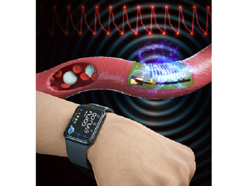 KAIST Team Develops Highly-Sensitive Wearable Piezoelectric Blood Pressure Sensor for Continuous Health Monitoring
- A collaborative research team led by KAIST Professor Keon Jae Lee verifies the accuracy of the highly-sensitive sensor through clinical trials
- Commercialization of the watch and patch-type sensor is in progress
A KAIST research team led by Professor Keon Jae Lee from the Department of Materials Science and Engineering and the College of Medicine of the Catholic University of Korea has developed a highly sensitive, wearable piezoelectric blood pressure sensor.
Blood pressure is a critical indicator for assessing general health and predicting stroke or heart failure. In particular, cardiovascular disease is the leading cause of global death, therefore, periodic measurement of blood pressure is crucial for personal healthcare.
Recently, there has been a growing interest in healthcare devices for continuous blood pressure monitoring. Although smart watches using LED-based photoplethysmography (PPG) technology have been on market, these devices have been limited by the accuracy constraints of optical sensors, making it hard to meet the international standards of automatic sphygmomanometers.
Professor Lee’s team has developed the wearable piezoelectric blood pressure sensor by transferring a highly sensitive, inorganic piezoelectric membrane from bulk sapphire substrates to flexible substrates. Ultrathin piezoelectric sensors with a thickness of several micrometers (one hundredth of the human hair) exhibit conformal contact with the skin to successfully collect accurate blood pressure from the subtle pulsation of the blood vessels.
Clinical trial at the St. Mary’s Hospital of the Catholic University validated the accuracy of blood pressure sensor at par with international standard with errors within ±5 mmHg and a standard deviation under 8 mmHg for both systolic and diastolic blood pressure. In addition, the research team successfully embedded the sensor on a watch-type product to enable continuous monitoring of blood pressure.
Prof. Keon Jae Lee said, “Major target of our healthcare devices is hypertensive patients for their daily medical check-up. We plan to develop a comfortable patch-type sensor to monitor blood pressure during sleep and have a start-up company commercialize these watch and patch-type products soon.”
This result titled “Clinical validation of wearable piezoelectric blood pressure sensor for health monitoring” was published in the online issue of Advanced Materials on March 24th, 2023. (DOI: 10.1002/adma.202301627)
Figure 1. Schematic illustration of the overall concept for a wearable piezoelectric blood pressure sensor (WPBPS).
Figure 2. Wearable piezoelectric blood pressure sensor (WPBPS) mounted on a watch (a) Schematic design of the WPBPS-embedded wristwatch. (b) Block diagram of the wireless communication circuit, which filters, amplifies, and transmits wireless data to portable devices. (c) Pulse waveforms transmitted from the wristwatch to the portable device by the wireless communication circuit. The inset shows a photograph of monitoring a user’s beat-to-beat pulses and their corresponding BP values in real time using the developed WPBPS-mounted wristwatch.
2023.04.17 View 8036
KAIST Team Develops Highly-Sensitive Wearable Piezoelectric Blood Pressure Sensor for Continuous Health Monitoring
- A collaborative research team led by KAIST Professor Keon Jae Lee verifies the accuracy of the highly-sensitive sensor through clinical trials
- Commercialization of the watch and patch-type sensor is in progress
A KAIST research team led by Professor Keon Jae Lee from the Department of Materials Science and Engineering and the College of Medicine of the Catholic University of Korea has developed a highly sensitive, wearable piezoelectric blood pressure sensor.
Blood pressure is a critical indicator for assessing general health and predicting stroke or heart failure. In particular, cardiovascular disease is the leading cause of global death, therefore, periodic measurement of blood pressure is crucial for personal healthcare.
Recently, there has been a growing interest in healthcare devices for continuous blood pressure monitoring. Although smart watches using LED-based photoplethysmography (PPG) technology have been on market, these devices have been limited by the accuracy constraints of optical sensors, making it hard to meet the international standards of automatic sphygmomanometers.
Professor Lee’s team has developed the wearable piezoelectric blood pressure sensor by transferring a highly sensitive, inorganic piezoelectric membrane from bulk sapphire substrates to flexible substrates. Ultrathin piezoelectric sensors with a thickness of several micrometers (one hundredth of the human hair) exhibit conformal contact with the skin to successfully collect accurate blood pressure from the subtle pulsation of the blood vessels.
Clinical trial at the St. Mary’s Hospital of the Catholic University validated the accuracy of blood pressure sensor at par with international standard with errors within ±5 mmHg and a standard deviation under 8 mmHg for both systolic and diastolic blood pressure. In addition, the research team successfully embedded the sensor on a watch-type product to enable continuous monitoring of blood pressure.
Prof. Keon Jae Lee said, “Major target of our healthcare devices is hypertensive patients for their daily medical check-up. We plan to develop a comfortable patch-type sensor to monitor blood pressure during sleep and have a start-up company commercialize these watch and patch-type products soon.”
This result titled “Clinical validation of wearable piezoelectric blood pressure sensor for health monitoring” was published in the online issue of Advanced Materials on March 24th, 2023. (DOI: 10.1002/adma.202301627)
Figure 1. Schematic illustration of the overall concept for a wearable piezoelectric blood pressure sensor (WPBPS).
Figure 2. Wearable piezoelectric blood pressure sensor (WPBPS) mounted on a watch (a) Schematic design of the WPBPS-embedded wristwatch. (b) Block diagram of the wireless communication circuit, which filters, amplifies, and transmits wireless data to portable devices. (c) Pulse waveforms transmitted from the wristwatch to the portable device by the wireless communication circuit. The inset shows a photograph of monitoring a user’s beat-to-beat pulses and their corresponding BP values in real time using the developed WPBPS-mounted wristwatch.
2023.04.17 View 8036 -
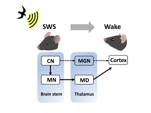 KAIST researchers discovers the neural circuit that reacts to alarm clock
KAIST (President Kwang Hyung Lee) announced on the 20th that a research team led by Professor Daesoo Kim of the Department of Brain and Cognitive Sciences and Dr. Jeongjin Kim 's team from the Korea Institute of Science and Technology (KIST) have identified the principle of awakening animals by responding to sounds even while sleeping.
Sleep is a very important physiological process that organizes brain activity and maintains health. During sleep, the function of sensory nerves is blocked, so the ability to detect danger in the proximity is reduced. However, many animals detect approaching predators and respond even while sleeping. Scientists thought that animals ready for danger by alternating between deep sleep and light sleep.
A research team led by Professor Daesoo Kim at KAIST discovered that animals have neural circuits that respond to sounds even during deep sleep. While awake, the medial geniculate thalamus responds to sounds, but during deep sleep, or Non-REM sleep, the Mediodorsal thalamus responds to sounds to wake up the brain.
As a result of the study, when the rats fell into deep sleep, the nerves of the medial geniculate thalamus were also sleeping, but the nerves of mediodorsal thalamus were awake and responded immediately to sounds. In addition, it was observed that when mediodorsal thalamus was inhibited, the rats could not wake up even when a sound was heard, and when the mediodorsal thalamus was stimulated, the rats woke up within a few seconds without sound.
This is the first study to show that sleep and wakefulness can transmit auditory signals through different neural circuits, and was reported in the international journal, Current Biology on February 7, and was highlighted by Nature. (https://www.nature.com/articles/d41586-023-00354-0)
Professor Daesoo Kim explained, “The findings of this study can used in developing digital healthcare technologies to be used to improve understanding of disorders of senses and wakefulness seen in various brain diseases and to control the senses in the future.”
This research was carried out with the support from the National Research Foundation of Korea's Mid-Career Research Foundation Program.
Figure 1. Traditionally, sound signals were thought to be propagated from the auditory nerve to the auditory thalamus. However, while in slow-wave sleep, the auditory nerve sends sound signals to the mediodorsal thalamic neurons via the brainstem nerve to induce arousal in the brain.
Figure 2. GRIK4 dorsomedial nerve in response to sound stimulation. The awakening effect is induced as the activity of the GRIK4 dorsal medial nerve increases based on the time when sound stimulation is given.
2023.03.03 View 5646
KAIST researchers discovers the neural circuit that reacts to alarm clock
KAIST (President Kwang Hyung Lee) announced on the 20th that a research team led by Professor Daesoo Kim of the Department of Brain and Cognitive Sciences and Dr. Jeongjin Kim 's team from the Korea Institute of Science and Technology (KIST) have identified the principle of awakening animals by responding to sounds even while sleeping.
Sleep is a very important physiological process that organizes brain activity and maintains health. During sleep, the function of sensory nerves is blocked, so the ability to detect danger in the proximity is reduced. However, many animals detect approaching predators and respond even while sleeping. Scientists thought that animals ready for danger by alternating between deep sleep and light sleep.
A research team led by Professor Daesoo Kim at KAIST discovered that animals have neural circuits that respond to sounds even during deep sleep. While awake, the medial geniculate thalamus responds to sounds, but during deep sleep, or Non-REM sleep, the Mediodorsal thalamus responds to sounds to wake up the brain.
As a result of the study, when the rats fell into deep sleep, the nerves of the medial geniculate thalamus were also sleeping, but the nerves of mediodorsal thalamus were awake and responded immediately to sounds. In addition, it was observed that when mediodorsal thalamus was inhibited, the rats could not wake up even when a sound was heard, and when the mediodorsal thalamus was stimulated, the rats woke up within a few seconds without sound.
This is the first study to show that sleep and wakefulness can transmit auditory signals through different neural circuits, and was reported in the international journal, Current Biology on February 7, and was highlighted by Nature. (https://www.nature.com/articles/d41586-023-00354-0)
Professor Daesoo Kim explained, “The findings of this study can used in developing digital healthcare technologies to be used to improve understanding of disorders of senses and wakefulness seen in various brain diseases and to control the senses in the future.”
This research was carried out with the support from the National Research Foundation of Korea's Mid-Career Research Foundation Program.
Figure 1. Traditionally, sound signals were thought to be propagated from the auditory nerve to the auditory thalamus. However, while in slow-wave sleep, the auditory nerve sends sound signals to the mediodorsal thalamic neurons via the brainstem nerve to induce arousal in the brain.
Figure 2. GRIK4 dorsomedial nerve in response to sound stimulation. The awakening effect is induced as the activity of the GRIK4 dorsal medial nerve increases based on the time when sound stimulation is given.
2023.03.03 View 5646 -
 A System for Stable Simultaneous Communication among Thousands of IoT Devices
A mmWave Backscatter System, developed by a team led by Professor Song Min Kim is exciting news for the IoT market as it will be able to provide fast and stable connectivity even for a massive network, which could finally allow IoT devices to reach their full potential.
A research team led by Professor Song Min Kim of the KAIST School of Electrical Engineering developed a system that can support concurrent communications for tens of millions of IoT devices using backscattering millimeter-level waves (mmWave).
With their mmWave backscatter method, the research team built a design enabling simultaneous signal demodulation in a complex environment for communication where tens of thousands of IoT devices are arranged indoors. The wide frequency range of mmWave exceeds 10GHz, which provides great scalability. In addition, backscattering reflects radiated signals instead of wirelessly creating its own, which allows operation at ultralow power. Therefore, the mmWave backscatter system offers internet connectivity on a mass scale to IoT devices at a low installation cost.
This research by Kangmin Bae et al. was presented at ACM MobiSys 2022. At this world-renowned conference for mobile systems, the research won the Best Paper Award under the title “OmniScatter: Sensitivity mmWave Backscattering Using Commodity FMCW Radar”. It is meaningful that members of the KAIST School of Electrical Engineering have won the Best Paper Award at ACM MobiSys for two consecutive years, as last year was the first time the award was presented to an institute from Asia.
IoT, as a core component of 5G/6G network, is showing exponential growth, and is expected to be part of a trillion devices by 2035. To support the connection of IoT devices on a mass scale, 5G and 6G each aim to support ten times and 100 times the network density of 4G, respectively. As a result, the importance of practical systems for large-scale communication has been raised.
The mmWave is a next-generation communication technology that can be incorporated in 5G/6G standards, as it utilizes carrier waves at frequencies between 30 to 300GHz. However, due to signal reduction at high frequencies and reflection loss, the current mmWave backscatter system enables communication in limited environments. In other words, it cannot operate in complex environments where various obstacles and reflectors are present. As a result, it is limited to the large-scale connection of IoT devices that require a relatively free arrangement.
The research team found the solution in the high coding gain of an FMCW radar. The team developed a signal processing method that can fundamentally separate backscatter signals from ambient noise while maintaining the coding gain of the radar. They achieved a receiver sensitivity of over 100 thousand times that of previously reported FMCW radars, which can support communication in practical environments. Additionally, given the radar’s property where the frequency of the demodulated signal changes depending on the physical location of the tag, the team designed a system that passively assigns them channels. This lets the ultralow-power backscatter communication system to take full advantage of the frequency range at 10 GHz or higher.
The developed system can use the radar of existing commercial products as gateway, making it easily compatible. In addition, since the backscatter system works at ultralow power levels of 10uW or below, it can operate for over 40 years with a single button cell and drastically reduce installation and maintenance costs.
The research team confirmed that mmWave backscatter devices arranged randomly in an office with various obstacles and reflectors could communicate effectively. The team then took things one step further and conducted a successful trace-driven evaluation where they simultaneously received information sent by 1,100 devices.
Their research presents connectivity that greatly exceeds network density required by next-generation communication like 5G and 6G. The system is expected to become a stepping stone for the hyper-connected future to come.
Professor Kim said, “mmWave backscatter is the technology we’ve dreamt of. The mass scalability and ultralow power at which it can operate IoT devices is unmatched by any existing technology”. He added, “We look forward to this system being actively utilized to enable the wide availability of IoT in the hyper-connected generation to come”.
To demonstrate the massive connectivity of the system, a trace-driven evaluation of 1,100 concurrent tag transmissions are made. Figure shows the demodulation result of each and every 1,100 tags as red triangles, where they successfully communicate without collision.
This work was supported by Samsung Research Funding & Incubation Center of Samsung Electronics and by the ITRC (Information Technology Research Center) support program supervised by the IITP (Institute of Information & Communications Technology Planning & Evaluation).
Profile: Song Min Kim, Ph.D.Professorsongmin@kaist.ac.krhttps://smile.kaist.ac.kr
SMILE Lab.School of Electrical Engineering
2022.07.28 View 9943
A System for Stable Simultaneous Communication among Thousands of IoT Devices
A mmWave Backscatter System, developed by a team led by Professor Song Min Kim is exciting news for the IoT market as it will be able to provide fast and stable connectivity even for a massive network, which could finally allow IoT devices to reach their full potential.
A research team led by Professor Song Min Kim of the KAIST School of Electrical Engineering developed a system that can support concurrent communications for tens of millions of IoT devices using backscattering millimeter-level waves (mmWave).
With their mmWave backscatter method, the research team built a design enabling simultaneous signal demodulation in a complex environment for communication where tens of thousands of IoT devices are arranged indoors. The wide frequency range of mmWave exceeds 10GHz, which provides great scalability. In addition, backscattering reflects radiated signals instead of wirelessly creating its own, which allows operation at ultralow power. Therefore, the mmWave backscatter system offers internet connectivity on a mass scale to IoT devices at a low installation cost.
This research by Kangmin Bae et al. was presented at ACM MobiSys 2022. At this world-renowned conference for mobile systems, the research won the Best Paper Award under the title “OmniScatter: Sensitivity mmWave Backscattering Using Commodity FMCW Radar”. It is meaningful that members of the KAIST School of Electrical Engineering have won the Best Paper Award at ACM MobiSys for two consecutive years, as last year was the first time the award was presented to an institute from Asia.
IoT, as a core component of 5G/6G network, is showing exponential growth, and is expected to be part of a trillion devices by 2035. To support the connection of IoT devices on a mass scale, 5G and 6G each aim to support ten times and 100 times the network density of 4G, respectively. As a result, the importance of practical systems for large-scale communication has been raised.
The mmWave is a next-generation communication technology that can be incorporated in 5G/6G standards, as it utilizes carrier waves at frequencies between 30 to 300GHz. However, due to signal reduction at high frequencies and reflection loss, the current mmWave backscatter system enables communication in limited environments. In other words, it cannot operate in complex environments where various obstacles and reflectors are present. As a result, it is limited to the large-scale connection of IoT devices that require a relatively free arrangement.
The research team found the solution in the high coding gain of an FMCW radar. The team developed a signal processing method that can fundamentally separate backscatter signals from ambient noise while maintaining the coding gain of the radar. They achieved a receiver sensitivity of over 100 thousand times that of previously reported FMCW radars, which can support communication in practical environments. Additionally, given the radar’s property where the frequency of the demodulated signal changes depending on the physical location of the tag, the team designed a system that passively assigns them channels. This lets the ultralow-power backscatter communication system to take full advantage of the frequency range at 10 GHz or higher.
The developed system can use the radar of existing commercial products as gateway, making it easily compatible. In addition, since the backscatter system works at ultralow power levels of 10uW or below, it can operate for over 40 years with a single button cell and drastically reduce installation and maintenance costs.
The research team confirmed that mmWave backscatter devices arranged randomly in an office with various obstacles and reflectors could communicate effectively. The team then took things one step further and conducted a successful trace-driven evaluation where they simultaneously received information sent by 1,100 devices.
Their research presents connectivity that greatly exceeds network density required by next-generation communication like 5G and 6G. The system is expected to become a stepping stone for the hyper-connected future to come.
Professor Kim said, “mmWave backscatter is the technology we’ve dreamt of. The mass scalability and ultralow power at which it can operate IoT devices is unmatched by any existing technology”. He added, “We look forward to this system being actively utilized to enable the wide availability of IoT in the hyper-connected generation to come”.
To demonstrate the massive connectivity of the system, a trace-driven evaluation of 1,100 concurrent tag transmissions are made. Figure shows the demodulation result of each and every 1,100 tags as red triangles, where they successfully communicate without collision.
This work was supported by Samsung Research Funding & Incubation Center of Samsung Electronics and by the ITRC (Information Technology Research Center) support program supervised by the IITP (Institute of Information & Communications Technology Planning & Evaluation).
Profile: Song Min Kim, Ph.D.Professorsongmin@kaist.ac.krhttps://smile.kaist.ac.kr
SMILE Lab.School of Electrical Engineering
2022.07.28 View 9943 -
 KAIST & LG U+ Team Up for Quantum Computing Solution for Ultra-Space 6G Satellite Networking
KAIST quantum computer scientists have optimized ultra-space 6G Low-Earth Orbit (LEO) satellite networking, finding the shortest path to transfer data from a city to another place via multi-satellite hops.
The research team led by Professor June-Koo Kevin Rhee and Professor Dongsu Han in partnership with LG U+ verified the possibility of ultra-performance and precision communication with satellite networks using D-Wave, the first commercialized quantum computer.
Satellite network optimization has remained challenging since the network needs to be reconfigured whenever satellites approach other satellites within the connection range in a three-dimensional space. Moreover, LEO satellites orbiting at 200~2000 km above the Earth change their positions dynamically, whereas Geo-Stationary Orbit (GSO) satellites do not change their positions. Thus, LEO satellite network optimization needs to be solved in real time.
The research groups formulated the problem as a Quadratic Unconstrained Binary Optimization (QUBO) problem and managed to solve the problem, incorporating the connectivity and link distance limits as the constraints.
The proposed optimization algorithm is reported to be much more efficient in terms of hop counts and path length than previously reported studies using classical solutions. These results verify that a satellite network can provide ultra-performance (over 1Gbps user-perceived speed), and ultra-precision (less than 5ms end-to-end latency) network services, which are comparable to terrestrial communication.
Once QUBO is applied, “ultra-space networking” is expected to be realized with 6G. Researchers said that an ultra-space network provides communication services for an object moving at up to 10 km altitude with an extreme speed (~ 1000 km/h). Optimized LEO satellite networks can provide 6G communication services to currently unavailable areas such as air flights and deserts.
Professor Rhee, who is also the CEO of Qunova Computing, noted, “Collaboration with LG U+ was meaningful as we were able to find an industrial application for a quantum computer. We look forward to more quantum application research on real problems such as in communications, drug and material discovery, logistics, and fintech industries.”
2022.06.17 View 8888
KAIST & LG U+ Team Up for Quantum Computing Solution for Ultra-Space 6G Satellite Networking
KAIST quantum computer scientists have optimized ultra-space 6G Low-Earth Orbit (LEO) satellite networking, finding the shortest path to transfer data from a city to another place via multi-satellite hops.
The research team led by Professor June-Koo Kevin Rhee and Professor Dongsu Han in partnership with LG U+ verified the possibility of ultra-performance and precision communication with satellite networks using D-Wave, the first commercialized quantum computer.
Satellite network optimization has remained challenging since the network needs to be reconfigured whenever satellites approach other satellites within the connection range in a three-dimensional space. Moreover, LEO satellites orbiting at 200~2000 km above the Earth change their positions dynamically, whereas Geo-Stationary Orbit (GSO) satellites do not change their positions. Thus, LEO satellite network optimization needs to be solved in real time.
The research groups formulated the problem as a Quadratic Unconstrained Binary Optimization (QUBO) problem and managed to solve the problem, incorporating the connectivity and link distance limits as the constraints.
The proposed optimization algorithm is reported to be much more efficient in terms of hop counts and path length than previously reported studies using classical solutions. These results verify that a satellite network can provide ultra-performance (over 1Gbps user-perceived speed), and ultra-precision (less than 5ms end-to-end latency) network services, which are comparable to terrestrial communication.
Once QUBO is applied, “ultra-space networking” is expected to be realized with 6G. Researchers said that an ultra-space network provides communication services for an object moving at up to 10 km altitude with an extreme speed (~ 1000 km/h). Optimized LEO satellite networks can provide 6G communication services to currently unavailable areas such as air flights and deserts.
Professor Rhee, who is also the CEO of Qunova Computing, noted, “Collaboration with LG U+ was meaningful as we were able to find an industrial application for a quantum computer. We look forward to more quantum application research on real problems such as in communications, drug and material discovery, logistics, and fintech industries.”
2022.06.17 View 8888 -
 SM CEP Soo-Man Lee to Teach at the KAIST School of Computing
The Founder and Chief Executive Producer of SM Entertainment Soo-Man Lee was appointed as a distinguished visiting professor in the KAIST School of Computing. His three-year term starts on March 1.
KAIST and the SM Entertainment signed an MOU on joint research on the metaverse last year and Lee’s appointment is the extension of their mutual collaborations in fields where technologies converge and will encourage innovative advancements in engineering technology and the entertainment industry.
Lee, who completed a graduate program in computer science at California State University Northridge will give special leadership lectures for both undergraduate and graduate students, and will participate in metaverse-related research as a consultant.
In particular, Professor Lee will participate in joint research with the tentatively named Metaverse Institute affiliated with the KAIST Institute for Artificial Intelligence. The institute will help SM Entertainment stay ahead of the global metaverse market by using the avatars of celebrities, and lend itself to raising the already strong brand power of the K-pop leader.
Professor Lee said, “I am grateful that KAIST, the very cradle of Korea’s science and technology, has given me the opportunity to meet its students as a visiting professor. We will lead the metaverse world, in which Korea is emerging as a market leader, with the excellent contents and technology unique to our country, and work together to lead the future global entertainment market.”
President Kwang-Hyung Lee said, “The ability to expand our limitless creativity in the metaverse is indispensable for us as we adapt to this new era. We hope that the vision and creative insights of Executive Producer Lee, which have allowed him to look ahead into the future of the entertainment contents market, will have a positive and fresh impact on the members of KAIST.”
The global influence and reputation of Executive Producer Lee has been well established through his various awards. He was the first Korean to be listed on Variety500 for five consecutive years from 2017 to 2021. He was also the first Korean awardee of the Asia Game Changer Awards in 2016, the first cultural figure to receive the YoungSan Diplomacy Award in 2017, the only Korean to be listed on the 2020 Billboard Impact List, and he has also received the K-pop Contribution Award at the 10th Gaon Chart Music Awards. He recently introduced Play2Create (P2C), a new interactive and creative culture in which re-creation can be enjoyed like a game using IP, and is leading the establishment of the P2C ecosystem.
2022.03.03 View 6160
SM CEP Soo-Man Lee to Teach at the KAIST School of Computing
The Founder and Chief Executive Producer of SM Entertainment Soo-Man Lee was appointed as a distinguished visiting professor in the KAIST School of Computing. His three-year term starts on March 1.
KAIST and the SM Entertainment signed an MOU on joint research on the metaverse last year and Lee’s appointment is the extension of their mutual collaborations in fields where technologies converge and will encourage innovative advancements in engineering technology and the entertainment industry.
Lee, who completed a graduate program in computer science at California State University Northridge will give special leadership lectures for both undergraduate and graduate students, and will participate in metaverse-related research as a consultant.
In particular, Professor Lee will participate in joint research with the tentatively named Metaverse Institute affiliated with the KAIST Institute for Artificial Intelligence. The institute will help SM Entertainment stay ahead of the global metaverse market by using the avatars of celebrities, and lend itself to raising the already strong brand power of the K-pop leader.
Professor Lee said, “I am grateful that KAIST, the very cradle of Korea’s science and technology, has given me the opportunity to meet its students as a visiting professor. We will lead the metaverse world, in which Korea is emerging as a market leader, with the excellent contents and technology unique to our country, and work together to lead the future global entertainment market.”
President Kwang-Hyung Lee said, “The ability to expand our limitless creativity in the metaverse is indispensable for us as we adapt to this new era. We hope that the vision and creative insights of Executive Producer Lee, which have allowed him to look ahead into the future of the entertainment contents market, will have a positive and fresh impact on the members of KAIST.”
The global influence and reputation of Executive Producer Lee has been well established through his various awards. He was the first Korean to be listed on Variety500 for five consecutive years from 2017 to 2021. He was also the first Korean awardee of the Asia Game Changer Awards in 2016, the first cultural figure to receive the YoungSan Diplomacy Award in 2017, the only Korean to be listed on the 2020 Billboard Impact List, and he has also received the K-pop Contribution Award at the 10th Gaon Chart Music Awards. He recently introduced Play2Create (P2C), a new interactive and creative culture in which re-creation can be enjoyed like a game using IP, and is leading the establishment of the P2C ecosystem.
2022.03.03 View 6160