Photodiode
-
 KAIST Develops Wearable Carbon Dioxide Sensor to Enable Real-time Apnea Diagnosis
- Professor Seunghyup Yoo’s research team of the School of Electrical Engineering developed an ultralow-power carbon dioxide (CO2) sensor using a flexible and thin organic photodiode, and succeeded in real-time breathing monitoring by attaching it to a commercial mask
- Wearable devices with features such as low power, high stability, and flexibility can be utilized for early diagnosis of various diseases such as chronic obstructive pulmonary disease and sleep apnea
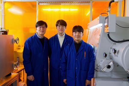
< Photo 1. From the left, School of Electrical Engineering, Ph.D. candidate DongHo Choi, Professor Seunghyup Yoo, and Department of Materials Science and Engineering, Bachelor’s candidate MinJae Kim >
Carbon dioxide (CO2) is a major respiratory metabolite, and continuous monitoring of CO2 concentration in exhaled breath is not only an important indicator for early detection and diagnosis of respiratory and circulatory system diseases, but can also be widely used for monitoring personal exercise status. KAIST researchers succeeded in accurately measuring CO2 concentration by attaching it to the inside of a mask.
KAIST (President Kwang-Hyung Lee) announced on February 10th that Professor Seunghyup Yoo's research team in the Department of Electrical and Electronic Engineering developed a low-power, high-speed wearable CO2 sensor capable of stable breathing monitoring in real time.
Existing non-invasive CO2 sensors had limitations in that they were large in size and consumed high power. In particular, optochemical CO2 sensors using fluorescent molecules have the advantage of being miniaturized and lightweight, but due to the photodegradation phenomenon of dye molecules, they are difficult to use stably for a long time, which limits their use as wearable healthcare sensors.
Optochemical CO2 sensors utilize the fact that the intensity of fluorescence emitted from fluorescent molecules decreases depending on the concentration of CO2, and it is important to effectively detect changes in fluorescence light.
To this end, the research team developed a low-power CO2 sensor consisting of an LED and an organic photodiode surrounding it. Based on high light collection efficiency, the sensor, which minimizes the amount of excitation light irradiated on fluorescent molecules, achieved a device power consumption of 171 μW, which is tens of times lower than existing sensors that consume several mW.
< Figure 1. Structure and operating principle of the developed optochemical carbon dioxide (CO2) sensor. Light emitted from the LED is converted into fluorescence through the fluorescent film, reflected from the light scattering layer, and incident on the organic photodiode. CO2 reacts with a small amount of water inside the fluorescent film to form carbonic acid (H2CO3), which increases the concentration of hydrogen ions (H+), and the fluorescence intensity due to 470 nm excitation light decreases. The circular organic photodiode with high light collection efficiency effectively detects changes in fluorescence intensity, lowers the power required light up the LED, and reduces light-induced deterioration. >
The research team also elucidated the photodegradation path of fluorescent molecules used in CO2 sensors, revealed the cause of the increase in error over time in photochemical sensors, and suggested an optical design method to suppress the occurrence of errors.
Based on this, the research team developed a sensor that effectively reduces errors caused by photodegradation, which was a chronic problem of existing photochemical sensors, and can be used continuously for up to 9 hours while existing technologies based on the same material can be used for less than 20 minutes, and can be used multiple times when replacing the CO2 detection fluorescent film.
< Figure 2. Wearable smart mask and real-time breathing monitoring. The fabricated sensor module consists of four elements (①: gas-permeable light-scattering layer, ②: color filter and organic photodiode, ③: light-emitting diode, ④: CO2-detecting fluorescent film). The thin and light sensor (D1: 400 nm, D2: 470 nm) is attached to the inside of the mask to monitor the wearer's breathing in real time. >
The developed sensor accurately measured CO2 concentration by being attached to the inside of a mask based on the advantages of being light (0.12 g), thin (0.7 mm), and flexible. In addition, it showed fast speed and high resolution that can monitor respiratory rate by distinguishing between inhalation and exhalation in real time.
< Photo 2. The developed sensor attached to the inside of the mask >
Professor Seunghyup Yoo said, "The developed sensor has excellent characteristics such as low power, high stability, and flexibility, so it can be widely applied to wearable devices, and can be used for the early diagnosis of various diseases such as hypercapnia, chronic obstructive pulmonary disease, and sleep apnea." He added, "In particular, it is expected to be used to improve side effects caused by rebreathing in environments where dust is generated or where masks are worn for long periods of time, such as during seasonal changes."
This study, in which KAIST's Department of Materials Science and Engineering's undergraduate student Minjae Kim and School of Electrical Engineering's doctoral student Dongho Choi participated as joint first authors, was published in the online version of Cell's sister journal, Device, on the 22nd of last month. (Paper title: Ultralow-power carbon dioxide sensor for real-time breath monitoring) DOI: https://doi.org/10.1016/j.device.2024.100681
< Photo 3. From the left, Professor Seunghyup Yoo of the School of Electrical Engineering, MinJae Kim, an undergraduate student in the Department of Materials Science and Engineering, and Dongho Choi, a doctoral student in the School of Electrical Engineering >
This study was supported by the Ministry of Trade, Industry and Energy's Materials and Components Technology Development Project, the National Research Foundation of Korea's Original Technology Development Project, and the KAIST Undergraduate Research Participation Project. This work was supported by the (URP) program.
2025.02.13 View 6676
KAIST Develops Wearable Carbon Dioxide Sensor to Enable Real-time Apnea Diagnosis
- Professor Seunghyup Yoo’s research team of the School of Electrical Engineering developed an ultralow-power carbon dioxide (CO2) sensor using a flexible and thin organic photodiode, and succeeded in real-time breathing monitoring by attaching it to a commercial mask
- Wearable devices with features such as low power, high stability, and flexibility can be utilized for early diagnosis of various diseases such as chronic obstructive pulmonary disease and sleep apnea
< Photo 1. From the left, School of Electrical Engineering, Ph.D. candidate DongHo Choi, Professor Seunghyup Yoo, and Department of Materials Science and Engineering, Bachelor’s candidate MinJae Kim >
Carbon dioxide (CO2) is a major respiratory metabolite, and continuous monitoring of CO2 concentration in exhaled breath is not only an important indicator for early detection and diagnosis of respiratory and circulatory system diseases, but can also be widely used for monitoring personal exercise status. KAIST researchers succeeded in accurately measuring CO2 concentration by attaching it to the inside of a mask.
KAIST (President Kwang-Hyung Lee) announced on February 10th that Professor Seunghyup Yoo's research team in the Department of Electrical and Electronic Engineering developed a low-power, high-speed wearable CO2 sensor capable of stable breathing monitoring in real time.
Existing non-invasive CO2 sensors had limitations in that they were large in size and consumed high power. In particular, optochemical CO2 sensors using fluorescent molecules have the advantage of being miniaturized and lightweight, but due to the photodegradation phenomenon of dye molecules, they are difficult to use stably for a long time, which limits their use as wearable healthcare sensors.
Optochemical CO2 sensors utilize the fact that the intensity of fluorescence emitted from fluorescent molecules decreases depending on the concentration of CO2, and it is important to effectively detect changes in fluorescence light.
To this end, the research team developed a low-power CO2 sensor consisting of an LED and an organic photodiode surrounding it. Based on high light collection efficiency, the sensor, which minimizes the amount of excitation light irradiated on fluorescent molecules, achieved a device power consumption of 171 μW, which is tens of times lower than existing sensors that consume several mW.
< Figure 1. Structure and operating principle of the developed optochemical carbon dioxide (CO2) sensor. Light emitted from the LED is converted into fluorescence through the fluorescent film, reflected from the light scattering layer, and incident on the organic photodiode. CO2 reacts with a small amount of water inside the fluorescent film to form carbonic acid (H2CO3), which increases the concentration of hydrogen ions (H+), and the fluorescence intensity due to 470 nm excitation light decreases. The circular organic photodiode with high light collection efficiency effectively detects changes in fluorescence intensity, lowers the power required light up the LED, and reduces light-induced deterioration. >
The research team also elucidated the photodegradation path of fluorescent molecules used in CO2 sensors, revealed the cause of the increase in error over time in photochemical sensors, and suggested an optical design method to suppress the occurrence of errors.
Based on this, the research team developed a sensor that effectively reduces errors caused by photodegradation, which was a chronic problem of existing photochemical sensors, and can be used continuously for up to 9 hours while existing technologies based on the same material can be used for less than 20 minutes, and can be used multiple times when replacing the CO2 detection fluorescent film.
< Figure 2. Wearable smart mask and real-time breathing monitoring. The fabricated sensor module consists of four elements (①: gas-permeable light-scattering layer, ②: color filter and organic photodiode, ③: light-emitting diode, ④: CO2-detecting fluorescent film). The thin and light sensor (D1: 400 nm, D2: 470 nm) is attached to the inside of the mask to monitor the wearer's breathing in real time. >
The developed sensor accurately measured CO2 concentration by being attached to the inside of a mask based on the advantages of being light (0.12 g), thin (0.7 mm), and flexible. In addition, it showed fast speed and high resolution that can monitor respiratory rate by distinguishing between inhalation and exhalation in real time.
< Photo 2. The developed sensor attached to the inside of the mask >
Professor Seunghyup Yoo said, "The developed sensor has excellent characteristics such as low power, high stability, and flexibility, so it can be widely applied to wearable devices, and can be used for the early diagnosis of various diseases such as hypercapnia, chronic obstructive pulmonary disease, and sleep apnea." He added, "In particular, it is expected to be used to improve side effects caused by rebreathing in environments where dust is generated or where masks are worn for long periods of time, such as during seasonal changes."
This study, in which KAIST's Department of Materials Science and Engineering's undergraduate student Minjae Kim and School of Electrical Engineering's doctoral student Dongho Choi participated as joint first authors, was published in the online version of Cell's sister journal, Device, on the 22nd of last month. (Paper title: Ultralow-power carbon dioxide sensor for real-time breath monitoring) DOI: https://doi.org/10.1016/j.device.2024.100681
< Photo 3. From the left, Professor Seunghyup Yoo of the School of Electrical Engineering, MinJae Kim, an undergraduate student in the Department of Materials Science and Engineering, and Dongho Choi, a doctoral student in the School of Electrical Engineering >
This study was supported by the Ministry of Trade, Industry and Energy's Materials and Components Technology Development Project, the National Research Foundation of Korea's Original Technology Development Project, and the KAIST Undergraduate Research Participation Project. This work was supported by the (URP) program.
2025.02.13 View 6676 -
 KAIST Secures Core Technology for Ultra-High-Resolution Image Sensors
A joint research team from Korea and the United States has developed next-generation, high-resolution image sensor technology with higher power efficiency and a smaller size compared to existing sensors. Notably, they have secured foundational technology for ultra-high-resolution shortwave infrared (SWIR) image sensors, an area currently dominated by Sony, paving the way for future market entry.
KAIST (represented by President Kwang Hyung Lee) announced on the 20th of November that a research team led by Professor SangHyeon Kim from the School of Electrical Engineering, in collaboration with Inha University and Yale University in the U.S., has developed an ultra-thin broadband photodiode (PD), marking a significant breakthrough in high-performance image sensor technology.
This research drastically improves the trade-off between the absorption layer thickness and quantum efficiency found in conventional photodiode technology. Specifically, it achieved high quantum efficiency of over 70% even in an absorption layer thinner than one micrometer (μm), reducing the thickness of the absorption layer by approximately 70% compared to existing technologies.
A thinner absorption layer simplifies pixel processing, allowing for higher resolution and smoother carrier diffusion, which is advantageous for light carrier acquisition while also reducing the cost. However, a fundamental issue with thinner absorption layers is the reduced absorption of long-wavelength light.
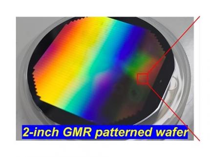
< Figure 1. Schematic diagram of the InGaAs photodiode image sensor integrated on the Guided-Mode Resonance (GMR) structure proposed in this study (left), a photograph of the fabricated wafer, and a scanning electron microscope (SEM) image of the periodic patterns (right) >
The research team introduced a guided-mode resonance (GMR) structure* that enables high-efficiency light absorption across a wide spectral range from 400 nanometers (nm) to 1,700 nanometers (nm). This wavelength range includes not only visible light but also light the SWIR region, making it valuable for various industrial applications.
*Guided-Mode Resonance (GMR) Structure: A concept used in electromagnetics, a phenomenon in which a specific (light) wave resonates (forming a strong electric/magnetic field) at a specific wavelength. Since energy is maximized under these conditions, it has been used to increase antenna or radar efficiency.
The improved performance in the SWIR region is expected to play a significant role in developing next-generation image sensors with increasingly high resolutions. The GMR structure, in particular, holds potential for further enhancing resolution and other performance metrics through hybrid integration and monolithic 3D integration with complementary metal-oxide-semiconductor (CMOS)-based readout integrated circuits (ROIC).
< Figure 2. Benchmark for state-of-the-art InGaAs-based SWIR pixels with simulated EQE lines as a function of TAL variation. Performance is maintained while reducing the absorption layer thickness from 2.1 micrometers or more to 1 micrometer or less while reducing it by 50% to 70% >
The research team has significantly enhanced international competitiveness in low-power devices and ultra-high-resolution imaging technology, opening up possibilities for applications in digital cameras, security systems, medical and industrial image sensors, as well as future ultra-high-resolution sensors for autonomous driving, aerospace, and satellite observation.
Professor Sang Hyun Kim, the lead researcher, commented, “This research demonstrates that significantly higher performance than existing technologies can be achieved even with ultra-thin absorption layers.”
< Figure 3. Top optical microscope image and cross-sectional scanning electron microscope image of the InGaAs photodiode image sensor fabricated on the GMR structure (left). Improved quantum efficiency performance of the ultra-thin image sensor (red) fabricated with the technology proposed in this study (right) >
The results of this research were published on 15th of November, in the prestigious international journal Light: Science & Applications (JCR 2.9%, IF=20.6), with Professor Dae-Myung Geum of Inha University (formerly a KAIST postdoctoral researcher) and Dr. Jinha Lim (currently a postdoctoral researcher at Yale University) as co-first authors. (Paper title: “Highly-efficient (>70%) and Wide-spectral (400 nm -1700 nm) sub-micron-thick InGaAs photodiodes for future high-resolution image sensors”)
This study was supported by the National Research Foundation of Korea.
2024.11.22 View 5533
KAIST Secures Core Technology for Ultra-High-Resolution Image Sensors
A joint research team from Korea and the United States has developed next-generation, high-resolution image sensor technology with higher power efficiency and a smaller size compared to existing sensors. Notably, they have secured foundational technology for ultra-high-resolution shortwave infrared (SWIR) image sensors, an area currently dominated by Sony, paving the way for future market entry.
KAIST (represented by President Kwang Hyung Lee) announced on the 20th of November that a research team led by Professor SangHyeon Kim from the School of Electrical Engineering, in collaboration with Inha University and Yale University in the U.S., has developed an ultra-thin broadband photodiode (PD), marking a significant breakthrough in high-performance image sensor technology.
This research drastically improves the trade-off between the absorption layer thickness and quantum efficiency found in conventional photodiode technology. Specifically, it achieved high quantum efficiency of over 70% even in an absorption layer thinner than one micrometer (μm), reducing the thickness of the absorption layer by approximately 70% compared to existing technologies.
A thinner absorption layer simplifies pixel processing, allowing for higher resolution and smoother carrier diffusion, which is advantageous for light carrier acquisition while also reducing the cost. However, a fundamental issue with thinner absorption layers is the reduced absorption of long-wavelength light.
< Figure 1. Schematic diagram of the InGaAs photodiode image sensor integrated on the Guided-Mode Resonance (GMR) structure proposed in this study (left), a photograph of the fabricated wafer, and a scanning electron microscope (SEM) image of the periodic patterns (right) >
The research team introduced a guided-mode resonance (GMR) structure* that enables high-efficiency light absorption across a wide spectral range from 400 nanometers (nm) to 1,700 nanometers (nm). This wavelength range includes not only visible light but also light the SWIR region, making it valuable for various industrial applications.
*Guided-Mode Resonance (GMR) Structure: A concept used in electromagnetics, a phenomenon in which a specific (light) wave resonates (forming a strong electric/magnetic field) at a specific wavelength. Since energy is maximized under these conditions, it has been used to increase antenna or radar efficiency.
The improved performance in the SWIR region is expected to play a significant role in developing next-generation image sensors with increasingly high resolutions. The GMR structure, in particular, holds potential for further enhancing resolution and other performance metrics through hybrid integration and monolithic 3D integration with complementary metal-oxide-semiconductor (CMOS)-based readout integrated circuits (ROIC).
< Figure 2. Benchmark for state-of-the-art InGaAs-based SWIR pixels with simulated EQE lines as a function of TAL variation. Performance is maintained while reducing the absorption layer thickness from 2.1 micrometers or more to 1 micrometer or less while reducing it by 50% to 70% >
The research team has significantly enhanced international competitiveness in low-power devices and ultra-high-resolution imaging technology, opening up possibilities for applications in digital cameras, security systems, medical and industrial image sensors, as well as future ultra-high-resolution sensors for autonomous driving, aerospace, and satellite observation.
Professor Sang Hyun Kim, the lead researcher, commented, “This research demonstrates that significantly higher performance than existing technologies can be achieved even with ultra-thin absorption layers.”
< Figure 3. Top optical microscope image and cross-sectional scanning electron microscope image of the InGaAs photodiode image sensor fabricated on the GMR structure (left). Improved quantum efficiency performance of the ultra-thin image sensor (red) fabricated with the technology proposed in this study (right) >
The results of this research were published on 15th of November, in the prestigious international journal Light: Science & Applications (JCR 2.9%, IF=20.6), with Professor Dae-Myung Geum of Inha University (formerly a KAIST postdoctoral researcher) and Dr. Jinha Lim (currently a postdoctoral researcher at Yale University) as co-first authors. (Paper title: “Highly-efficient (>70%) and Wide-spectral (400 nm -1700 nm) sub-micron-thick InGaAs photodiodes for future high-resolution image sensors”)
This study was supported by the National Research Foundation of Korea.
2024.11.22 View 5533