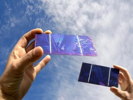
Photocurrent
-
 KAIST Captures Hot Holes: A Breakthrough in Light-to-Electricity Energy Conversion
When light interacts with metallic nanostructures, it instantaneously generates plasmonic hot carriers, which serve as key intermediates for converting optical energy into high-value energy sources such as electricity and chemical energy. Among these, hot holes play a crucial role in enhancing photoelectrochemical reactions. However, they thermally dissipate within picoseconds (trillionths of a second), making practical applications challenging. Now, a Korean research team has successfully developed a method for sustaining hot holes longer and amplifying their flow, accelerating the commercialization of next-generation, high-efficiency, light-to-energy conversion technologies.
KAIST (represented by President Kwang Hyung Lee) announced on the 12th of March that a research team led by Distinguished Professor Jeong Young Park from the Department of Chemistry, in collaboration with Professor Moonsang Lee from the Department of Materials Science and Engineering at Inha University, has successfully amplified the flow of hot holes and mapped local current distribution in real time, thereby elucidating the mechanism of photocurrent enhancement.
The team designed a nanodiode structure by placing a metallic nanomesh on a specialized semiconductor substrate (p-type gallium nitride) to facilitate hot hole extraction at the surface. As a result, in gallium nitride substrates aligned with the hot hole extraction direction, the flow of hot holes was amplified by approximately two times compared to substrates aligned in other directions.
To fabricate the Au nanomesh, a polystyrene nano-bead monolayer assembly was first placed on a gallium nitride (p-GaN) substrate, and then the polystyrene nano-beads were etched to form a nanomesh template (Figure 1A). Then, a 20 nm thick gold nano-film was deposited, and the etched polystyrene nano-beads were removed to realize the gold nano-mesh structure on the GaN substrate (Figure 1B). The fabricated Au nanomesh exhibited strong light absorption in the visible range due to the plasmonic resonance effect (Figure 1C). >
Furthermore, using a photoconductive atomic force microscopy (pc-AFM)-based photocurrent mapping system, the researchers analyzed the flow of hot holes in real time at the nanometer scale (one hundred-thousandth the thickness of a human hair). They observed that hot hole activation was strongest at "hot spots," where light was locally concentrated on the gold nanomesh. However, by modifying the growth direction of the gallium nitride substrate, hot hole activation extended beyond the hot spots to other areas as well.
Through this research, the team discovered an efficient method for converting light into electrical and chemical energy. This breakthrough is expected to significantly advance next-generation solar cells, photocatalysts, and hydrogen production technologies.
Professor Jeong Young Park stated, "For the first time, we have successfully controlled the flow of hot holes using a nanodiode technique. This innovation holds great potential for various optoelectronic devices and photocatalytic applications. For example, it could lead to groundbreaking advancements in solar energy conversion technologies, such as solar cells and hydrogen production. Additionally, the real-time analysis technology we developed can be applied to the development of ultra-miniaturized optoelectronic devices, including optical sensors and nanoscale semiconductor components."
The study was led by Hyunhwa Lee (PhD., KAIST Department of Chemistry) and Yujin Park (Postdoc Researcher, University of Texas at Austin Department of Chemical Engineering) as co-first authors and Professors Moonsang Lee (Inha University, Department of Materials Science and Engineering) and Jeong Young Park (KAIST, Department of Chemistry) serving as corresponding authors. The research findings were published online in Science Advances on March 7.
(Paper Title: “Reconfiguring hot-hole flux via polarity modulation of p-GaN in plasmonic Schottky architectures”, DOI: https://www.science.org/doi/10.1126/sciadv.adu0086)
This research was supported by the National Research Foundation of Korea (NRF).
2025.03.17 View 3817
KAIST Captures Hot Holes: A Breakthrough in Light-to-Electricity Energy Conversion
When light interacts with metallic nanostructures, it instantaneously generates plasmonic hot carriers, which serve as key intermediates for converting optical energy into high-value energy sources such as electricity and chemical energy. Among these, hot holes play a crucial role in enhancing photoelectrochemical reactions. However, they thermally dissipate within picoseconds (trillionths of a second), making practical applications challenging. Now, a Korean research team has successfully developed a method for sustaining hot holes longer and amplifying their flow, accelerating the commercialization of next-generation, high-efficiency, light-to-energy conversion technologies.
KAIST (represented by President Kwang Hyung Lee) announced on the 12th of March that a research team led by Distinguished Professor Jeong Young Park from the Department of Chemistry, in collaboration with Professor Moonsang Lee from the Department of Materials Science and Engineering at Inha University, has successfully amplified the flow of hot holes and mapped local current distribution in real time, thereby elucidating the mechanism of photocurrent enhancement.
The team designed a nanodiode structure by placing a metallic nanomesh on a specialized semiconductor substrate (p-type gallium nitride) to facilitate hot hole extraction at the surface. As a result, in gallium nitride substrates aligned with the hot hole extraction direction, the flow of hot holes was amplified by approximately two times compared to substrates aligned in other directions.
To fabricate the Au nanomesh, a polystyrene nano-bead monolayer assembly was first placed on a gallium nitride (p-GaN) substrate, and then the polystyrene nano-beads were etched to form a nanomesh template (Figure 1A). Then, a 20 nm thick gold nano-film was deposited, and the etched polystyrene nano-beads were removed to realize the gold nano-mesh structure on the GaN substrate (Figure 1B). The fabricated Au nanomesh exhibited strong light absorption in the visible range due to the plasmonic resonance effect (Figure 1C). >
Furthermore, using a photoconductive atomic force microscopy (pc-AFM)-based photocurrent mapping system, the researchers analyzed the flow of hot holes in real time at the nanometer scale (one hundred-thousandth the thickness of a human hair). They observed that hot hole activation was strongest at "hot spots," where light was locally concentrated on the gold nanomesh. However, by modifying the growth direction of the gallium nitride substrate, hot hole activation extended beyond the hot spots to other areas as well.
Through this research, the team discovered an efficient method for converting light into electrical and chemical energy. This breakthrough is expected to significantly advance next-generation solar cells, photocatalysts, and hydrogen production technologies.
Professor Jeong Young Park stated, "For the first time, we have successfully controlled the flow of hot holes using a nanodiode technique. This innovation holds great potential for various optoelectronic devices and photocatalytic applications. For example, it could lead to groundbreaking advancements in solar energy conversion technologies, such as solar cells and hydrogen production. Additionally, the real-time analysis technology we developed can be applied to the development of ultra-miniaturized optoelectronic devices, including optical sensors and nanoscale semiconductor components."
The study was led by Hyunhwa Lee (PhD., KAIST Department of Chemistry) and Yujin Park (Postdoc Researcher, University of Texas at Austin Department of Chemical Engineering) as co-first authors and Professors Moonsang Lee (Inha University, Department of Materials Science and Engineering) and Jeong Young Park (KAIST, Department of Chemistry) serving as corresponding authors. The research findings were published online in Science Advances on March 7.
(Paper Title: “Reconfiguring hot-hole flux via polarity modulation of p-GaN in plasmonic Schottky architectures”, DOI: https://www.science.org/doi/10.1126/sciadv.adu0086)
This research was supported by the National Research Foundation of Korea (NRF).
2025.03.17 View 3817 -
 KAIST Researchers Introduce New and Improved, Next-Generation Perovskite Solar Cell
- KAIST-Yonsei university researchers developed innovative dipole technology to maximize near-infrared photon harvesting efficiency
- Overcoming the shortcoming of existing perovskite solar cells that cannot utilize approximately 52% of total solar energy
- Development of next-generation solar cell technology with high efficiency and high stability that can absorb near-infrared light beyond the existing visible light range with a perovskite-dipole-organic semiconductor hybrid structure
< Photo. (From left) Professor Jung-Yong Lee, Ph.D. candidate Min-Ho Lee, and Master’s candidate Min Seok Kim of the School of Electrical Engineering >
Existing perovskite solar cells, which have the problem of not being able to utilize approximately 52% of total solar energy, have been developed by a Korean research team as an innovative technology that maximizes near-infrared light capture performance while greatly improving power conversion efficiency. This greatly increases the possibility of commercializing next-generation solar cells and is expected to contribute to important technological advancements in the global solar cell market.
The research team of Professor Jung-Yong Lee of the School of Electrical Engineering at KAIST (President Kwang-Hyung Lee) and Professor Woojae Kim of the Department of Chemistry at Yonsei University announced on October 31st that they have developed a high-efficiency and high-stability organic-inorganic hybrid solar cell production technology that maximizes near-infrared light capture beyond the existing visible light range.
The research team suggested and advanced a hybrid next-generation device structure with organic photo-semiconductors that complements perovskite materials limited to visible light absorption and expands the absorption range to near-infrared.
In addition, they revealed the electronic structure problem that mainly occurs in the structure and announced a high-performance solar cell device that dramatically solved this problem by introducing a dipole layer*.
*Dipole layer: A thin material layer that controls the energy level within the device to facilitate charge transport and forms an interface potential difference to improve device performance.
Existing lead-based perovskite solar cells have a problem in that their absorption spectrum is limited to the visible light region with a wavelength of 850 nanometers (nm) or less, which prevents them from utilizing approximately 52% of the total solar energy.
To solve this problem, the research team designed a hybrid device that combined an organic bulk heterojunction (BHJ) with perovskite and implemented a solar cell that can absorb up to the near-infrared region.
In particular, by introducing a sub-nanometer dipole interface layer, they succeeded in alleviating the energy barrier between the perovskite and the organic bulk heterojunction (BHJ), suppressing charge accumulation, maximizing the contribution to the near-infrared, and improving the current density (JSC) to 4.9 mA/cm².
The key achievement of this study is that the power conversion efficiency (PCE) of the hybrid device has been significantly increased from 20.4% to 24.0%. In particular, this study achieved a high internal quantum efficiency (IQE) compared to previous studies, reaching 78% in the near-infrared region.
< Figure. The illustration of the mechanism of improving the electronic structure and charge transfer capability through Perovskite/organic hybrid device structure and dipole interfacial layers (DILs). The proposed dipole interfacial layer forms a strong interfacial dipole, effectively reducing the energy barrier between the perovskite and organic bulk heterojunction (BHJ), and suppressing hole accumulation. This technology improves near-infrared photon harvesting and charge transfer, and as a result, the power conversion efficiency of the solar cell increases to 24.0%. In addition, it achieves excellent stability by maintaining performance for 1,200 hours even in an extremely humid environment. >
In addition, this device showed high stability, showing excellent results of maintaining more than 80% of the initial efficiency in the maximum output tracking for more than 800 hours even under extreme humidity conditions.
Professor Jung-Yong Lee said, “Through this study, we have effectively solved the charge accumulation and energy band mismatch problems faced by existing perovskite/organic hybrid solar cells, and we will be able to significantly improve the power conversion efficiency while maximizing the near-infrared light capture performance, which will be a new breakthrough that can solve the mechanical-chemical stability problems of existing perovskites and overcome the optical limitations.”
This study, in which KAIST School of Electrical Engineering Ph.D. candidate Min-Ho Lee and Master's candidate Min Seok Kim participated as co-first authors, was published in the September 30th online edition of the international academic journal Advanced Materials. (Paper title: Suppressing Hole Accumulation Through Sub-Nanometer Dipole Interfaces in Hybrid Perovskite/Organic Solar Cells for Boosting Near-Infrared Photon Harvesting).
This study was conducted with the support of the National Research Foundation of Korea.
2024.10.31 View 6853
KAIST Researchers Introduce New and Improved, Next-Generation Perovskite Solar Cell
- KAIST-Yonsei university researchers developed innovative dipole technology to maximize near-infrared photon harvesting efficiency
- Overcoming the shortcoming of existing perovskite solar cells that cannot utilize approximately 52% of total solar energy
- Development of next-generation solar cell technology with high efficiency and high stability that can absorb near-infrared light beyond the existing visible light range with a perovskite-dipole-organic semiconductor hybrid structure
< Photo. (From left) Professor Jung-Yong Lee, Ph.D. candidate Min-Ho Lee, and Master’s candidate Min Seok Kim of the School of Electrical Engineering >
Existing perovskite solar cells, which have the problem of not being able to utilize approximately 52% of total solar energy, have been developed by a Korean research team as an innovative technology that maximizes near-infrared light capture performance while greatly improving power conversion efficiency. This greatly increases the possibility of commercializing next-generation solar cells and is expected to contribute to important technological advancements in the global solar cell market.
The research team of Professor Jung-Yong Lee of the School of Electrical Engineering at KAIST (President Kwang-Hyung Lee) and Professor Woojae Kim of the Department of Chemistry at Yonsei University announced on October 31st that they have developed a high-efficiency and high-stability organic-inorganic hybrid solar cell production technology that maximizes near-infrared light capture beyond the existing visible light range.
The research team suggested and advanced a hybrid next-generation device structure with organic photo-semiconductors that complements perovskite materials limited to visible light absorption and expands the absorption range to near-infrared.
In addition, they revealed the electronic structure problem that mainly occurs in the structure and announced a high-performance solar cell device that dramatically solved this problem by introducing a dipole layer*.
*Dipole layer: A thin material layer that controls the energy level within the device to facilitate charge transport and forms an interface potential difference to improve device performance.
Existing lead-based perovskite solar cells have a problem in that their absorption spectrum is limited to the visible light region with a wavelength of 850 nanometers (nm) or less, which prevents them from utilizing approximately 52% of the total solar energy.
To solve this problem, the research team designed a hybrid device that combined an organic bulk heterojunction (BHJ) with perovskite and implemented a solar cell that can absorb up to the near-infrared region.
In particular, by introducing a sub-nanometer dipole interface layer, they succeeded in alleviating the energy barrier between the perovskite and the organic bulk heterojunction (BHJ), suppressing charge accumulation, maximizing the contribution to the near-infrared, and improving the current density (JSC) to 4.9 mA/cm².
The key achievement of this study is that the power conversion efficiency (PCE) of the hybrid device has been significantly increased from 20.4% to 24.0%. In particular, this study achieved a high internal quantum efficiency (IQE) compared to previous studies, reaching 78% in the near-infrared region.
< Figure. The illustration of the mechanism of improving the electronic structure and charge transfer capability through Perovskite/organic hybrid device structure and dipole interfacial layers (DILs). The proposed dipole interfacial layer forms a strong interfacial dipole, effectively reducing the energy barrier between the perovskite and organic bulk heterojunction (BHJ), and suppressing hole accumulation. This technology improves near-infrared photon harvesting and charge transfer, and as a result, the power conversion efficiency of the solar cell increases to 24.0%. In addition, it achieves excellent stability by maintaining performance for 1,200 hours even in an extremely humid environment. >
In addition, this device showed high stability, showing excellent results of maintaining more than 80% of the initial efficiency in the maximum output tracking for more than 800 hours even under extreme humidity conditions.
Professor Jung-Yong Lee said, “Through this study, we have effectively solved the charge accumulation and energy band mismatch problems faced by existing perovskite/organic hybrid solar cells, and we will be able to significantly improve the power conversion efficiency while maximizing the near-infrared light capture performance, which will be a new breakthrough that can solve the mechanical-chemical stability problems of existing perovskites and overcome the optical limitations.”
This study, in which KAIST School of Electrical Engineering Ph.D. candidate Min-Ho Lee and Master's candidate Min Seok Kim participated as co-first authors, was published in the September 30th online edition of the international academic journal Advanced Materials. (Paper title: Suppressing Hole Accumulation Through Sub-Nanometer Dipole Interfaces in Hybrid Perovskite/Organic Solar Cells for Boosting Near-Infrared Photon Harvesting).
This study was conducted with the support of the National Research Foundation of Korea.
2024.10.31 View 6853