Optical
-
 KAIST Develops Virtual Staining Technology for 3D Histopathology
Moving beyond traditional methods of observing thinly sliced and stained cancer tissues, a collaborative international research team led by KAIST has successfully developed a groundbreaking technology. This innovation uses advanced optical techniques combined with an artificial intelligence-based deep learning algorithm to create realistic, virtually stained 3D images of cancer tissue without the need for serial sectioning nor staining. This breakthrough is anticipated to pave the way for next-generation non-invasive pathological diagnosis.
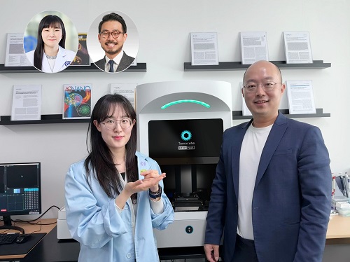
< Photo 1. (From left) Juyeon Park (Ph.D. Candidate, Department of Physics), Professor YongKeun Park (Department of Physics) (Top left) Professor Su-Jin Shin (Gangnam Severance Hospital), Professor Tae Hyun Hwang (Vanderbilt University School of Medicine) >
KAIST (President Kwang Hyung Lee) announced on the 26th that a research team led by Professor YongKeun Park of the Department of Physics, in collaboration with Professor Su-Jin Shin's team at Yonsei University Gangnam Severance Hospital, Professor Tae Hyun Hwang's team at Mayo Clinic, and Tomocube's AI research team, has developed an innovative technology capable of vividly displaying the 3D structure of cancer tissues without separate staining.
For over 200 years, conventional pathology has relied on observing cancer tissues under a microscope, a method that only shows specific cross-sections of the 3D cancer tissue. This has limited the ability to understand the three-dimensional connections and spatial arrangements between cells.
To overcome this, the research team utilized holotomography (HT), an advanced optical technology, to measure the 3D refractive index information of tissues. They then integrated an AI-based deep learning algorithm to successfully generate virtual H&E* images.* H&E (Hematoxylin & Eosin): The most widely used staining method for observing pathological tissues. Hematoxylin stains cell nuclei blue, and eosin stains cytoplasm pink.
The research team quantitatively demonstrated that the images generated by this technology are highly similar to actual stained tissue images. Furthermore, the technology exhibited consistent performance across various organs and tissues, proving its versatility and reliability as a next-generation pathological analysis tool.
< Figure 1. Comparison of conventional 3D tissue pathology procedure and the 3D virtual H&E staining technology proposed in this study. The traditional method requires preparing and staining dozens of tissue slides, while the proposed technology can reduce the number of slides by up to 10 times and quickly generate H&E images without the staining process. >
Moreover, by validating the feasibility of this technology through joint research with hospitals and research institutions in Korea and the United States, utilizing Tomocube's holotomography equipment, the team demonstrated its potential for full-scale adoption in real-world pathological research settings.
Professor YongKeun Park stated, "This research marks a major advancement by transitioning pathological analysis from conventional 2D methods to comprehensive 3D imaging. It will greatly enhance biomedical research and clinical diagnostics, particularly in understanding cancer tumor boundaries and the intricate spatial arrangements of cells within tumor microenvironments."
< Figure 2. Results of AI-based 3D virtual H&E staining and quantitative analysis of pathological tissue. The virtually stained images enabled 3D reconstruction of key pathological features such as cell nuclei and glandular lumens. Based on this, various quantitative indicators, including cell nuclear distribution, volume, and surface area, could be extracted. >
This research, with Juyeon Park, a student of the Integrated Master’s and Ph.D. Program at KAIST, as the first author, was published online in the prestigious journal Nature Communications on May 22.
(Paper title: Revealing 3D microanatomical structures of unlabeled thick cancer tissues using holotomography and virtual H&E staining.
[https://doi.org/10.1038/s41467-025-59820-0]
This study was supported by the Leader Researcher Program of the National Research Foundation of Korea, the Global Industry Technology Cooperation Center Project of the Korea Institute for Advancement of Technology, and the Korea Health Industry Development Institute.
2025.05.26 View 2621
KAIST Develops Virtual Staining Technology for 3D Histopathology
Moving beyond traditional methods of observing thinly sliced and stained cancer tissues, a collaborative international research team led by KAIST has successfully developed a groundbreaking technology. This innovation uses advanced optical techniques combined with an artificial intelligence-based deep learning algorithm to create realistic, virtually stained 3D images of cancer tissue without the need for serial sectioning nor staining. This breakthrough is anticipated to pave the way for next-generation non-invasive pathological diagnosis.
< Photo 1. (From left) Juyeon Park (Ph.D. Candidate, Department of Physics), Professor YongKeun Park (Department of Physics) (Top left) Professor Su-Jin Shin (Gangnam Severance Hospital), Professor Tae Hyun Hwang (Vanderbilt University School of Medicine) >
KAIST (President Kwang Hyung Lee) announced on the 26th that a research team led by Professor YongKeun Park of the Department of Physics, in collaboration with Professor Su-Jin Shin's team at Yonsei University Gangnam Severance Hospital, Professor Tae Hyun Hwang's team at Mayo Clinic, and Tomocube's AI research team, has developed an innovative technology capable of vividly displaying the 3D structure of cancer tissues without separate staining.
For over 200 years, conventional pathology has relied on observing cancer tissues under a microscope, a method that only shows specific cross-sections of the 3D cancer tissue. This has limited the ability to understand the three-dimensional connections and spatial arrangements between cells.
To overcome this, the research team utilized holotomography (HT), an advanced optical technology, to measure the 3D refractive index information of tissues. They then integrated an AI-based deep learning algorithm to successfully generate virtual H&E* images.* H&E (Hematoxylin & Eosin): The most widely used staining method for observing pathological tissues. Hematoxylin stains cell nuclei blue, and eosin stains cytoplasm pink.
The research team quantitatively demonstrated that the images generated by this technology are highly similar to actual stained tissue images. Furthermore, the technology exhibited consistent performance across various organs and tissues, proving its versatility and reliability as a next-generation pathological analysis tool.
< Figure 1. Comparison of conventional 3D tissue pathology procedure and the 3D virtual H&E staining technology proposed in this study. The traditional method requires preparing and staining dozens of tissue slides, while the proposed technology can reduce the number of slides by up to 10 times and quickly generate H&E images without the staining process. >
Moreover, by validating the feasibility of this technology through joint research with hospitals and research institutions in Korea and the United States, utilizing Tomocube's holotomography equipment, the team demonstrated its potential for full-scale adoption in real-world pathological research settings.
Professor YongKeun Park stated, "This research marks a major advancement by transitioning pathological analysis from conventional 2D methods to comprehensive 3D imaging. It will greatly enhance biomedical research and clinical diagnostics, particularly in understanding cancer tumor boundaries and the intricate spatial arrangements of cells within tumor microenvironments."
< Figure 2. Results of AI-based 3D virtual H&E staining and quantitative analysis of pathological tissue. The virtually stained images enabled 3D reconstruction of key pathological features such as cell nuclei and glandular lumens. Based on this, various quantitative indicators, including cell nuclear distribution, volume, and surface area, could be extracted. >
This research, with Juyeon Park, a student of the Integrated Master’s and Ph.D. Program at KAIST, as the first author, was published online in the prestigious journal Nature Communications on May 22.
(Paper title: Revealing 3D microanatomical structures of unlabeled thick cancer tissues using holotomography and virtual H&E staining.
[https://doi.org/10.1038/s41467-025-59820-0]
This study was supported by the Leader Researcher Program of the National Research Foundation of Korea, the Global Industry Technology Cooperation Center Project of the Korea Institute for Advancement of Technology, and the Korea Health Industry Development Institute.
2025.05.26 View 2621 -
 KAIST Innovates Mid-Infrared Photodetectors for Exoplanet Detection, Expanding Applications to Environmental and Medical Fields
NASA’s James Webb Space Telescope (JWST) utilizes mid-infrared spectroscopy to precisely analyze molecular components such as water vapor and sulfur dioxide in exoplanet atmospheres. The key to this analysis, where each molecule exhibits a unique spectral "fingerprint," lies in highly sensitive photodetector technology capable of measuring extremely weak light intensities. Recently, KAIST researchers have developed an innovative photodetector capable of detecting a broad range of mid-infrared spectra, garnering significant attention.
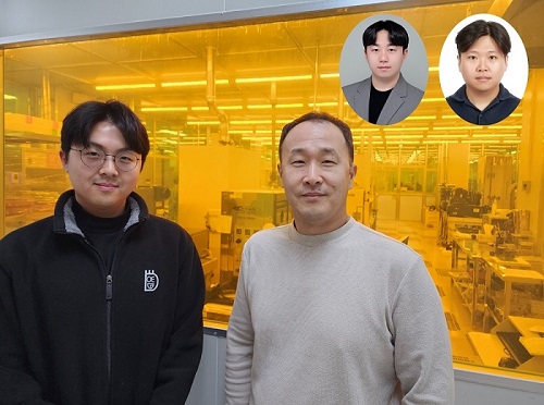
< Photo 1. (from the left) Ph.D. candidate Inki Kim (co-author), Professor SangHyeon Kim (corresponding author), Dr. Joonsup Shim (first author), and Dr. Jinha Lim (co-author) of KAIST School of Electrical Engineering. >
KAIST (represented by President Kwang-Hyung Lee) announced on the 27th of March that a research team led by Professor SangHyeon Kim from the School of Electrical Engineering has developed a mid-infrared photodetector that operates stably at room temperature, marking a major turning point for the commercialization of ultra-compact optical sensors.
The newly developed photodetector utilizes conventional silicon-based CMOS processes, enabling low-cost mass production while maintaining stable operation at room temperature. Notably, the research team successfully demonstrated the real-time detection of carbon dioxide (CO₂) gas using ultra-compact and ultra-thin optical sensors equipped with this photodetector, proving its potential for environmental monitoring and hazardous gas analysis.
Existing mid-infrared photodetectors generally require cooling systems due to high thermal noise at room temperature. These cooling systems increase the size and cost of equipment, making miniaturization and integration into portable devices challenging. Furthermore, conventional mid-infrared photodetectors are incompatible with silicon-based CMOS processes, limiting large-scale production and commercialization.
To address these limitations, the research team developed a waveguide-integrated photodetector using germanium (Ge), a Group IV element like silicon. This approach enables broad-spectrum mid-infrared detection while ensuring stable operation at room temperature.
< Figure 1. Schematic diagram of a room-temperature mid-infrared waveguide-integrated photodetector based on the Ge-on-insulator optical platform proposed in this study (top). Optical microscope image of the integrated photodetector connected with the sensing unit (bottom). >
A waveguide is a structure designed to efficiently guide light along a specific path with minimal loss. To implement various optical functions on a chip (on-chip), the development of waveguide-integrated photodetectors and waveguide-based optical components is essential.
Unlike conventional photodetectors that primarily rely on bandgap absorption principles, this new technology leverages the bolometric effect*, allowing it to detect the entire mid-infrared spectral range. As a result, it can be widely applied to the real-time sensing of various molecular species.
*Bolometric effect: A principle in which light absorption leads to an increase in temperature, causing electrical signals to change accordingly.
The waveguide-integrated mid-infrared photodetector developed by the research team is considered a groundbreaking innovation that overcomes the limitations of existing mid-infrared sensor technologies, including the need for cooling, difficulties in mass production, and high costs.
< Figure 2. Room temperature photoresponse characteristics of the mid-infrared waveguide photodetector proposed in this study (left) and real-time carbon dioxide (CO2) gas sensing results using the photodetector (right). >
This breakthrough technology is expected to be applicable across diverse fields, including environmental monitoring, medical diagnostics, industrial process management, national defense and security, and smart devices. It also paves the way for next-generation mid-infrared sensor advancements.
Professor SangHyeon Kim from KAIST stated, "This research represents a novel approach that overcomes the limitations of existing mid-infrared photodetector technologies and has great potential for practical applications in various fields." He further emphasized, "Since this sensor technology is compatible with CMOS processes, it enables low-cost mass production, making it highly suitable for next-generation environmental monitoring systems and smart manufacturing sites."
< Figure 3. Performance comparison image of a room-temperature mid-infrared waveguide photodetector fabricated with the technology proposed in this study. It achieves the world’s highest performance compared to existing technologies utilizing the Bolometric effect, and is the only solution compatible with CMOS processes. The technology proposed by our research team is characterized by its ability to respond to a wide spectrum of the mid-infrared band without limitations. >
The study, with Dr. Joonsup Shim (currently a postdoctoral researcher at Harvard University) as the first author, was published on March 19, 2025 in the internationally renowned journal Light: Science & Applications (JCR 2.9%, IF=20.6).
(Paper title: “Room-temperature waveguide-integrated photodetector using bolometric effect for mid-infrared spectroscopy applications,” https://doi.org/10.1038/s41377-025-01803-3)
2025.03.27 View 2660
KAIST Innovates Mid-Infrared Photodetectors for Exoplanet Detection, Expanding Applications to Environmental and Medical Fields
NASA’s James Webb Space Telescope (JWST) utilizes mid-infrared spectroscopy to precisely analyze molecular components such as water vapor and sulfur dioxide in exoplanet atmospheres. The key to this analysis, where each molecule exhibits a unique spectral "fingerprint," lies in highly sensitive photodetector technology capable of measuring extremely weak light intensities. Recently, KAIST researchers have developed an innovative photodetector capable of detecting a broad range of mid-infrared spectra, garnering significant attention.
< Photo 1. (from the left) Ph.D. candidate Inki Kim (co-author), Professor SangHyeon Kim (corresponding author), Dr. Joonsup Shim (first author), and Dr. Jinha Lim (co-author) of KAIST School of Electrical Engineering. >
KAIST (represented by President Kwang-Hyung Lee) announced on the 27th of March that a research team led by Professor SangHyeon Kim from the School of Electrical Engineering has developed a mid-infrared photodetector that operates stably at room temperature, marking a major turning point for the commercialization of ultra-compact optical sensors.
The newly developed photodetector utilizes conventional silicon-based CMOS processes, enabling low-cost mass production while maintaining stable operation at room temperature. Notably, the research team successfully demonstrated the real-time detection of carbon dioxide (CO₂) gas using ultra-compact and ultra-thin optical sensors equipped with this photodetector, proving its potential for environmental monitoring and hazardous gas analysis.
Existing mid-infrared photodetectors generally require cooling systems due to high thermal noise at room temperature. These cooling systems increase the size and cost of equipment, making miniaturization and integration into portable devices challenging. Furthermore, conventional mid-infrared photodetectors are incompatible with silicon-based CMOS processes, limiting large-scale production and commercialization.
To address these limitations, the research team developed a waveguide-integrated photodetector using germanium (Ge), a Group IV element like silicon. This approach enables broad-spectrum mid-infrared detection while ensuring stable operation at room temperature.
< Figure 1. Schematic diagram of a room-temperature mid-infrared waveguide-integrated photodetector based on the Ge-on-insulator optical platform proposed in this study (top). Optical microscope image of the integrated photodetector connected with the sensing unit (bottom). >
A waveguide is a structure designed to efficiently guide light along a specific path with minimal loss. To implement various optical functions on a chip (on-chip), the development of waveguide-integrated photodetectors and waveguide-based optical components is essential.
Unlike conventional photodetectors that primarily rely on bandgap absorption principles, this new technology leverages the bolometric effect*, allowing it to detect the entire mid-infrared spectral range. As a result, it can be widely applied to the real-time sensing of various molecular species.
*Bolometric effect: A principle in which light absorption leads to an increase in temperature, causing electrical signals to change accordingly.
The waveguide-integrated mid-infrared photodetector developed by the research team is considered a groundbreaking innovation that overcomes the limitations of existing mid-infrared sensor technologies, including the need for cooling, difficulties in mass production, and high costs.
< Figure 2. Room temperature photoresponse characteristics of the mid-infrared waveguide photodetector proposed in this study (left) and real-time carbon dioxide (CO2) gas sensing results using the photodetector (right). >
This breakthrough technology is expected to be applicable across diverse fields, including environmental monitoring, medical diagnostics, industrial process management, national defense and security, and smart devices. It also paves the way for next-generation mid-infrared sensor advancements.
Professor SangHyeon Kim from KAIST stated, "This research represents a novel approach that overcomes the limitations of existing mid-infrared photodetector technologies and has great potential for practical applications in various fields." He further emphasized, "Since this sensor technology is compatible with CMOS processes, it enables low-cost mass production, making it highly suitable for next-generation environmental monitoring systems and smart manufacturing sites."
< Figure 3. Performance comparison image of a room-temperature mid-infrared waveguide photodetector fabricated with the technology proposed in this study. It achieves the world’s highest performance compared to existing technologies utilizing the Bolometric effect, and is the only solution compatible with CMOS processes. The technology proposed by our research team is characterized by its ability to respond to a wide spectrum of the mid-infrared band without limitations. >
The study, with Dr. Joonsup Shim (currently a postdoctoral researcher at Harvard University) as the first author, was published on March 19, 2025 in the internationally renowned journal Light: Science & Applications (JCR 2.9%, IF=20.6).
(Paper title: “Room-temperature waveguide-integrated photodetector using bolometric effect for mid-infrared spectroscopy applications,” https://doi.org/10.1038/s41377-025-01803-3)
2025.03.27 View 2660 -
 KAIST Develops Janus-like Metasurface Technology that Acts According to the Direction of Light
Metasurface technology is an advanced optical technology that is thinner, lighter, and capable of precisely controlling light through nanometer-sized artificial structures compared to conventional technologies. KAIST researchers have overcome the limitations of existing metasurface technologies and successfully designed a Janus metasurface capable of perfectly controlling asymmetric light transmission. By applying this technology, they also proposed an innovative method to significantly enhance security by only decoding information under specific conditions.
KAIST (represented by President Kwang Hyung Lee) announced on the 15th of October that a research team led by Professor Jonghwa Shin from the Department of Materials Science and Engineering had developed a Janus metasurface capable of perfectly controlling asymmetric light transmission.
Asymmetric properties, which react differently depending on the direction, play a crucial role in various fields of science and engineering. The Janus metasurface developed by the research team implements an optical system capable of performing different functions in both directions.
Like the Roman god Janus with two faces, this metasurface shows entirely different optical responses depending on the direction of incoming light, effectively operating two independent optical systems with a single device (for example, a metasurface that acts as a magnifying lens in one direction and as a polarized camera in the other). In other words, by using this technology, it's possible to operate two different optical systems (e.g., a lens and a hologram) depending on the direction of the light.
This achievement addresses a challenge that existing metasurface technologies had not resolved. Conventional metasurface technology had limitations in selectively controlling the three properties of light—intensity, phase, and polarization—based on the direction of incidence.
The research team proposed a solution based on mathematical and physical principles, and succeeded in experimentally implementing different vector holograms in both directions. Through this achievement, they showcased a complete asymmetric light transmission control technology.
< Figure 1. Schematics of a device featuring asymmetric transmission. a) Device operating as a magnifying lens for back-side illumination. b) Device operating as a polarization camera for front-side illumination. >
Additionally, the research team developed a new optical encryption technology based on this metasurface technology. By using the Janus metasurface, they implemented a vector hologram that generates different images depending on the direction and polarization state of incoming light, showcasing an optical encryption system that significantly enhances security by allowing information to be decoded only under specific conditions.
This technology is expected to serve as a next-generation security solution, applicable in various fields such as quantum communication and secure data transmission.
Furthermore, the ultra-thin structure of the metasurface is expected to significantly reduce the volume and weight of traditional optical devices, contributing greatly to the miniaturization and lightweight design of next-generation devices.
< Figure 2. Experimental demonstration of Janus vectorial holograms. With front illuminations, vector images of the butterfly and the grasshopper are created, and with the back-side illuminations, vector images of the ladybug and the beetle are created. >
Professor Jonghwa Shin from the Department of Materials Science and Engineering at KAIST stated, "This research has enabled the complete asymmetric transmission control of light’s intensity, phase, and polarization, which has been a long-standing challenge in optics. It has opened up the possibility of developing various applied optical devices." He added, "We plan to continue developing optical devices that can be applied to various fields such as augmented reality (AR), holographic displays, and LiDAR systems for autonomous vehicles, utilizing the full potential of metasurface technology."
This research, in which Hyeonhee Kim (a doctoral student in the Department of Materials Science and Engineering at KAIST) and Joonkyo Jung participated as co-first authors, was published online in the international journal Advanced Materials and is scheduled to be published in the October 31 issue. (Title of the paper: "Bidirectional Vectorial Holography Using Bi-Layer Metasurfaces and Its Application to Optical Encryption")
The research was supported by the Nano Materials Technology Development Program and the Mid-Career Researcher Program of the National Research Foundation of Korea.
2024.10.15 View 4034
KAIST Develops Janus-like Metasurface Technology that Acts According to the Direction of Light
Metasurface technology is an advanced optical technology that is thinner, lighter, and capable of precisely controlling light through nanometer-sized artificial structures compared to conventional technologies. KAIST researchers have overcome the limitations of existing metasurface technologies and successfully designed a Janus metasurface capable of perfectly controlling asymmetric light transmission. By applying this technology, they also proposed an innovative method to significantly enhance security by only decoding information under specific conditions.
KAIST (represented by President Kwang Hyung Lee) announced on the 15th of October that a research team led by Professor Jonghwa Shin from the Department of Materials Science and Engineering had developed a Janus metasurface capable of perfectly controlling asymmetric light transmission.
Asymmetric properties, which react differently depending on the direction, play a crucial role in various fields of science and engineering. The Janus metasurface developed by the research team implements an optical system capable of performing different functions in both directions.
Like the Roman god Janus with two faces, this metasurface shows entirely different optical responses depending on the direction of incoming light, effectively operating two independent optical systems with a single device (for example, a metasurface that acts as a magnifying lens in one direction and as a polarized camera in the other). In other words, by using this technology, it's possible to operate two different optical systems (e.g., a lens and a hologram) depending on the direction of the light.
This achievement addresses a challenge that existing metasurface technologies had not resolved. Conventional metasurface technology had limitations in selectively controlling the three properties of light—intensity, phase, and polarization—based on the direction of incidence.
The research team proposed a solution based on mathematical and physical principles, and succeeded in experimentally implementing different vector holograms in both directions. Through this achievement, they showcased a complete asymmetric light transmission control technology.
< Figure 1. Schematics of a device featuring asymmetric transmission. a) Device operating as a magnifying lens for back-side illumination. b) Device operating as a polarization camera for front-side illumination. >
Additionally, the research team developed a new optical encryption technology based on this metasurface technology. By using the Janus metasurface, they implemented a vector hologram that generates different images depending on the direction and polarization state of incoming light, showcasing an optical encryption system that significantly enhances security by allowing information to be decoded only under specific conditions.
This technology is expected to serve as a next-generation security solution, applicable in various fields such as quantum communication and secure data transmission.
Furthermore, the ultra-thin structure of the metasurface is expected to significantly reduce the volume and weight of traditional optical devices, contributing greatly to the miniaturization and lightweight design of next-generation devices.
< Figure 2. Experimental demonstration of Janus vectorial holograms. With front illuminations, vector images of the butterfly and the grasshopper are created, and with the back-side illuminations, vector images of the ladybug and the beetle are created. >
Professor Jonghwa Shin from the Department of Materials Science and Engineering at KAIST stated, "This research has enabled the complete asymmetric transmission control of light’s intensity, phase, and polarization, which has been a long-standing challenge in optics. It has opened up the possibility of developing various applied optical devices." He added, "We plan to continue developing optical devices that can be applied to various fields such as augmented reality (AR), holographic displays, and LiDAR systems for autonomous vehicles, utilizing the full potential of metasurface technology."
This research, in which Hyeonhee Kim (a doctoral student in the Department of Materials Science and Engineering at KAIST) and Joonkyo Jung participated as co-first authors, was published online in the international journal Advanced Materials and is scheduled to be published in the October 31 issue. (Title of the paper: "Bidirectional Vectorial Holography Using Bi-Layer Metasurfaces and Its Application to Optical Encryption")
The research was supported by the Nano Materials Technology Development Program and the Mid-Career Researcher Program of the National Research Foundation of Korea.
2024.10.15 View 4034 -
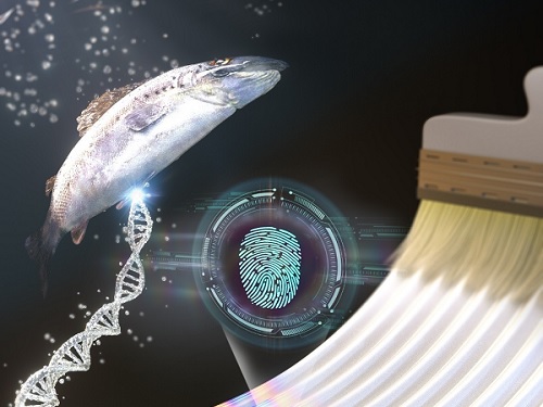 KAIST research team develops a forgery prevention technique using salmon DNA
The authenticity scandal that plagued the artwork “Beautiful Woman” by Kyung-ja Chun for 30 years shows how concerns about replicas can become a burden to artists, as most of them are not experts in the field of anti-counterfeiting. To solve this problem, artist-friendly physical unclonable functions (PUFs) based on optical techniques instead of electronic ones, which can be applied immediately onto artwork through brushstrokes are needed.
On May 23, a KAIST research team led by Professor Dong Ki Yoon in the Department of Chemistry revealed the development of a proprietary technology for security and certification using random patterns that occur during the self-assembly of soft materials.
With the development of the Internet of Things in recent years, various electronic devices and services can now be connected to the internet and carry out new innovative functions. However, counterfeiting technologies that infringe on individuals’ privacy have also entered the marketplace.
The technique developed by the research team involves random and spontaneous patterns that naturally occur during the self-assembly of two different types of soft materials, which can be used in the same way as human fingerprints for non-replicable security. This is very significant in that even non-experts in the field of security can construct anti-counterfeiting systems through simple actions like drawing a picture.
The team developed two unique methods. The first method uses liquid crystals. When liquid crystals become trapped in patterned substrates, they induce the symmetrical destruction of the structure and create a maze-like topology (Figure 1). The research team defined the pathways open to the right as 0 (blue), and those open to the left as 1 (red), and confirmed that the structure could be converted into a digital code composed of 0’s and 1’s that can serve as a type of fingerprint through object recognition using machine learning. This groundbreaking technique can be utilized by non-experts, as it does not require complex semiconductor patterns that are required by existing technology, and can be observed through the level of resolution of a smartphone camera. In particular, this technique can reconstruct information more easily than conventional methods that use semiconductor chips.
< Figure 1. Security technology using the maze made up of magnetically-assembled structures formed on a substrate patterned with liquid crystal materials. >
The second method uses DNA extracted from salmon. The DNA can be dissolved in water and applied with a brush to induce bulking instability, which forms random patterns similar to a zebra’s stripes. Here, the patterns create ridge endings and bifurcation, which are characteristics in fingerprints, and these can also be digitalized into 0’s and 1’s through machine learning. The research team applied conventional fingerprint recognition technology to this patterning technique and demonstrated its use as an artificial fingerprint. This method can be easily carried out using a brush, and the solution can be mixed into various colors and used as a new security ink.
< Figure 2. Technology to produce security ink using DNA polymers extracted from salmon >
This new security technology developed by the research team uses only simple organic materials and requires basic manufacturing processes, making it possible to enhance security at a low cost. In addition, users can produce patterns in the shapes and sizes they want, and even if the patterns are made in the same way, their randomness makes each individual pattern different. This provides high levels of security and gives the technique enhanced marketability.
Professor Dong Ki Yoon said, “These studies have taken the randomness that naturally occurs during self-assembly to create non-replicable patterns that can act like human fingerprints.” He added, “These ideas will be the cornerstone of technology that applies the many randomities that exist in nature to security systems.”
The two studies were published in the journal Advanced Materials under the titles “1Planar Spin Glass with Topologically-Protected Mazes in the Liquid Crystal Targeting for Reconfigurable Micro Security Media” and “2Paintable Physical Unclonable Function Using DNA” on May 6 and 5, respectively.
Author Information: 1Geonhyeong Park, Yun-Seok Choi, S. Joon Kwon*, and Dong Ki Yoon*/ 2Soon Mo Park†, Geonhyeong Park†, Dong Ki Yoon*: †co-first authors, *corresponding author
This research was funded by the Center for Multiscale Chiral Architectures and supported by the Ministry of Science and ICT-Korea Research Foundation, BRIDGE Convergent Research and Development Program, the Running Together Project, and the Samsung Future Technology Development Program.
< Figure 1-1. A scene from the schematic animation of the process of Blues (0) and Reds (1) forming the PUF by exploring the maze. From "Planar Spin Glass with Topologically-Protected Mazes in the Liquid Crystal Targeting for Reconfigurable Micro Security Media" by Geonhyeong Park, Yun-Seok Choi, S. Joon Kwon, Dong Ki Yoon. https://doi.org/10.1002/adma.202303077 >
< Figure 2-1. A schematic diagram of the formation of digital fingerprints formed using the DNA ink. From "Paintable Physical Unclonable Function Using DNA" by Soon Mo Park, Geonhyeong Park, Dong Ki Yoon. https://doi.org/10.1002/adma.202302135 >
2023.06.08 View 8521
KAIST research team develops a forgery prevention technique using salmon DNA
The authenticity scandal that plagued the artwork “Beautiful Woman” by Kyung-ja Chun for 30 years shows how concerns about replicas can become a burden to artists, as most of them are not experts in the field of anti-counterfeiting. To solve this problem, artist-friendly physical unclonable functions (PUFs) based on optical techniques instead of electronic ones, which can be applied immediately onto artwork through brushstrokes are needed.
On May 23, a KAIST research team led by Professor Dong Ki Yoon in the Department of Chemistry revealed the development of a proprietary technology for security and certification using random patterns that occur during the self-assembly of soft materials.
With the development of the Internet of Things in recent years, various electronic devices and services can now be connected to the internet and carry out new innovative functions. However, counterfeiting technologies that infringe on individuals’ privacy have also entered the marketplace.
The technique developed by the research team involves random and spontaneous patterns that naturally occur during the self-assembly of two different types of soft materials, which can be used in the same way as human fingerprints for non-replicable security. This is very significant in that even non-experts in the field of security can construct anti-counterfeiting systems through simple actions like drawing a picture.
The team developed two unique methods. The first method uses liquid crystals. When liquid crystals become trapped in patterned substrates, they induce the symmetrical destruction of the structure and create a maze-like topology (Figure 1). The research team defined the pathways open to the right as 0 (blue), and those open to the left as 1 (red), and confirmed that the structure could be converted into a digital code composed of 0’s and 1’s that can serve as a type of fingerprint through object recognition using machine learning. This groundbreaking technique can be utilized by non-experts, as it does not require complex semiconductor patterns that are required by existing technology, and can be observed through the level of resolution of a smartphone camera. In particular, this technique can reconstruct information more easily than conventional methods that use semiconductor chips.
< Figure 1. Security technology using the maze made up of magnetically-assembled structures formed on a substrate patterned with liquid crystal materials. >
The second method uses DNA extracted from salmon. The DNA can be dissolved in water and applied with a brush to induce bulking instability, which forms random patterns similar to a zebra’s stripes. Here, the patterns create ridge endings and bifurcation, which are characteristics in fingerprints, and these can also be digitalized into 0’s and 1’s through machine learning. The research team applied conventional fingerprint recognition technology to this patterning technique and demonstrated its use as an artificial fingerprint. This method can be easily carried out using a brush, and the solution can be mixed into various colors and used as a new security ink.
< Figure 2. Technology to produce security ink using DNA polymers extracted from salmon >
This new security technology developed by the research team uses only simple organic materials and requires basic manufacturing processes, making it possible to enhance security at a low cost. In addition, users can produce patterns in the shapes and sizes they want, and even if the patterns are made in the same way, their randomness makes each individual pattern different. This provides high levels of security and gives the technique enhanced marketability.
Professor Dong Ki Yoon said, “These studies have taken the randomness that naturally occurs during self-assembly to create non-replicable patterns that can act like human fingerprints.” He added, “These ideas will be the cornerstone of technology that applies the many randomities that exist in nature to security systems.”
The two studies were published in the journal Advanced Materials under the titles “1Planar Spin Glass with Topologically-Protected Mazes in the Liquid Crystal Targeting for Reconfigurable Micro Security Media” and “2Paintable Physical Unclonable Function Using DNA” on May 6 and 5, respectively.
Author Information: 1Geonhyeong Park, Yun-Seok Choi, S. Joon Kwon*, and Dong Ki Yoon*/ 2Soon Mo Park†, Geonhyeong Park†, Dong Ki Yoon*: †co-first authors, *corresponding author
This research was funded by the Center for Multiscale Chiral Architectures and supported by the Ministry of Science and ICT-Korea Research Foundation, BRIDGE Convergent Research and Development Program, the Running Together Project, and the Samsung Future Technology Development Program.
< Figure 1-1. A scene from the schematic animation of the process of Blues (0) and Reds (1) forming the PUF by exploring the maze. From "Planar Spin Glass with Topologically-Protected Mazes in the Liquid Crystal Targeting for Reconfigurable Micro Security Media" by Geonhyeong Park, Yun-Seok Choi, S. Joon Kwon, Dong Ki Yoon. https://doi.org/10.1002/adma.202303077 >
< Figure 2-1. A schematic diagram of the formation of digital fingerprints formed using the DNA ink. From "Paintable Physical Unclonable Function Using DNA" by Soon Mo Park, Geonhyeong Park, Dong Ki Yoon. https://doi.org/10.1002/adma.202302135 >
2023.06.08 View 8521 -
 Using light to throw and catch atoms to open up a new chapter for quantum computing
The technology to move and arrange atoms, the most basic component of a quantum computer, is very important to Rydberg quantum computing research. However, to place the atoms at the desired location, the atoms must be captured and transported one by one using a highly focused laser beam, commonly referred to as an optical tweezer. and, the quantum information of the atoms is likely to change midway.
KAIST (President Kwang Hyung Lee) announced on the 27th that a research team led by Professor Jaewook Ahn of the Department of Physics developed a technology to throw and receive rubidium atoms one by one using a laser beam.
The research team developed a method to throw and receive atoms which would minimize the time the optical tweezers are in contact with the atoms in which the quantum information the atoms carry may change. The research team used the characteristic that the rubidium atoms, which are kept at a very low temperature of 40μK below absolute zero, move very sensitively to the electromagnetic force applied by light along the focal point of the light tweezers.
The research team accelerated the laser of an optical tweezer to give an optical kick to an atom to send it to a target, then caught the flying atom with another optical tweezer to stop it. The atom flew at a speed of 65 cm/s, and traveled up to 4.2 μm. Compared to the existing technique of guiding the atoms with the optical tweezers, the technique of throwing and receiving atoms eliminates the need to calculate the transporting path for the tweezers, and makes it easier to fix the defects in the atomic arrangement. As a result, it is effective in generating and maintaining a large number of atomic arrangements, and when the technology is used to throw and receive flying atom qubits, it will be used in studying new and more powerful quantum computing methods that presupposes the structural changes in quantum arrangements.
"This technology will be used to develop larger and more powerful Rydberg quantum computers," says Professor Jaewook Ahn. “In a Rydberg quantum computer,” he continues, “atoms are arranged to store quantum information and interact with neighboring atoms through electromagnetic forces to perform quantum computing. The method of throwing an atom away for quick reconstruction the quantum array can be an effective way to fix an error in a quantum computer that requires a removal or replacement of an atom.”
The research, which was conducted by doctoral students Hansub Hwang and Andrew Byun of the Department of Physics at KAIST and Sylvain de Léséleuc, a researcher at the National Institute of Natural Sciences in Japan, was published in the international journal, Optica, 0n March 9th. (Paper title: Optical tweezers throw and catch single atoms).
This research was carried out with the support of the Samsung Science & Technology Foundation.
<Figure 1> A schematic diagram of the atom catching and throwing technique. The optical tweezer on the left kicks the atom to throw it into a trajectory to have the tweezer on the right catch it to stop it.
2023.03.28 View 7824
Using light to throw and catch atoms to open up a new chapter for quantum computing
The technology to move and arrange atoms, the most basic component of a quantum computer, is very important to Rydberg quantum computing research. However, to place the atoms at the desired location, the atoms must be captured and transported one by one using a highly focused laser beam, commonly referred to as an optical tweezer. and, the quantum information of the atoms is likely to change midway.
KAIST (President Kwang Hyung Lee) announced on the 27th that a research team led by Professor Jaewook Ahn of the Department of Physics developed a technology to throw and receive rubidium atoms one by one using a laser beam.
The research team developed a method to throw and receive atoms which would minimize the time the optical tweezers are in contact with the atoms in which the quantum information the atoms carry may change. The research team used the characteristic that the rubidium atoms, which are kept at a very low temperature of 40μK below absolute zero, move very sensitively to the electromagnetic force applied by light along the focal point of the light tweezers.
The research team accelerated the laser of an optical tweezer to give an optical kick to an atom to send it to a target, then caught the flying atom with another optical tweezer to stop it. The atom flew at a speed of 65 cm/s, and traveled up to 4.2 μm. Compared to the existing technique of guiding the atoms with the optical tweezers, the technique of throwing and receiving atoms eliminates the need to calculate the transporting path for the tweezers, and makes it easier to fix the defects in the atomic arrangement. As a result, it is effective in generating and maintaining a large number of atomic arrangements, and when the technology is used to throw and receive flying atom qubits, it will be used in studying new and more powerful quantum computing methods that presupposes the structural changes in quantum arrangements.
"This technology will be used to develop larger and more powerful Rydberg quantum computers," says Professor Jaewook Ahn. “In a Rydberg quantum computer,” he continues, “atoms are arranged to store quantum information and interact with neighboring atoms through electromagnetic forces to perform quantum computing. The method of throwing an atom away for quick reconstruction the quantum array can be an effective way to fix an error in a quantum computer that requires a removal or replacement of an atom.”
The research, which was conducted by doctoral students Hansub Hwang and Andrew Byun of the Department of Physics at KAIST and Sylvain de Léséleuc, a researcher at the National Institute of Natural Sciences in Japan, was published in the international journal, Optica, 0n March 9th. (Paper title: Optical tweezers throw and catch single atoms).
This research was carried out with the support of the Samsung Science & Technology Foundation.
<Figure 1> A schematic diagram of the atom catching and throwing technique. The optical tweezer on the left kicks the atom to throw it into a trajectory to have the tweezer on the right catch it to stop it.
2023.03.28 View 7824 -
 Atomically-Smooth Gold Crystals Help to Compress Light for Nanophotonic Applications
Highly compressed mid-infrared optical waves in a thin dielectric crystal on monocrystalline gold substrate investigated for the first time using a high-resolution scattering-type scanning near-field optical microscope.
KAIST researchers and their collaborators at home and abroad have successfully demonstrated a new platform for guiding the compressed light waves in very thin van der Waals crystals. Their method to guide the mid-infrared light with minimal loss will provide a breakthrough for the practical applications of ultra-thin dielectric crystals in next-generation optoelectronic devices based on strong light-matter interactions at the nanoscale.
Phonon-polaritons are collective oscillations of ions in polar dielectrics coupled to electromagnetic waves of light, whose electromagnetic field is much more compressed compared to the light wavelength. Recently, it was demonstrated that the phonon-polaritons in thin van der Waals crystals can be compressed even further when the material is placed on top of a highly conductive metal. In such a configuration, charges in the polaritonic crystal are “reflected” in the metal, and their coupling with light results in a new type of polariton waves called the image phonon-polaritons. Highly compressed image modes provide strong light-matter interactions, but are very sensitive to the substrate roughness, which hinders their practical application.
Challenged by these limitations, four research groups combined their efforts to develop a unique experimental platform using advanced fabrication and measurement methods. Their findings were published in Science Advances on July 13.
A KAIST research team led by Professor Min Seok Jang from the School of Electrical Engineering used a highly sensitive scanning near-field optical microscope (SNOM) to directly measure the optical fields of the hyperbolic image phonon-polaritons (HIP) propagating in a 63 nm-thick slab of hexagonal boron nitride (h-BN) on a monocrystalline gold substrate, showing the mid-infrared light waves in dielectric crystal compressed by a hundred times.
Professor Jang and a research professor in his group, Sergey Menabde, successfully obtained direct images of HIP waves propagating for many wavelengths, and detected a signal from the ultra-compressed high-order HIP in a regular h-BN crystals for the first time. They showed that the phonon-polaritons in van der Waals crystals can be significantly more compressed without sacrificing their lifetime.
This became possible due to the atomically-smooth surfaces of the home-grown gold crystals used as a substrate for the h-BN. Practically zero surface scattering and extremely small ohmic loss in gold at mid-infrared frequencies provide a low-loss environment for the HIP propagation. The HIP mode probed by the researchers was 2.4 times more compressed and yet exhibited a similar lifetime compared to the phonon-polaritons with a low-loss dielectric substrate, resulting in a twice higher figure of merit in terms of the normalized propagation length.
The ultra-smooth monocrystalline gold flakes used in the experiment were chemically grown by the team of Professor N. Asger Mortensen from the Center for Nano Optics at the University of Southern Denmark.
Mid-infrared spectrum is particularly important for sensing applications since many important organic molecules have absorption lines in the mid-infrared. However, a large number of molecules is required by the conventional detection methods for successful operation, whereas the ultra-compressed phonon-polariton fields can provide strong light-matter interactions at the microscopic level, thus significantly improving the detection limit down to a single molecule. The long lifetime of the HIP on monocrystalline gold will further improve the detection performance.
Furthermore, the study conducted by Professor Jang and the team demonstrated the striking similarity between the HIP and the image graphene plasmons. Both image modes possess significantly more confined electromagnetic field, yet their lifetime remains unaffected by the shorter polariton wavelength. This observation provides a broader perspective on image polaritons in general, and highlights their superiority in terms of the nanolight waveguiding compared to the conventional low-dimensional polaritons in van der Waals crystals on a dielectric substrate.
Professor Jang said, “Our research demonstrated the advantages of image polaritons, and especially the image phonon-polaritons. These optical modes can be used in the future optoelectronic devices where both the low-loss propagation and the strong light-matter interaction are necessary. I hope that our results will pave the way for the realization of more efficient nanophotonic devices such as metasurfaces, optical switches, sensors, and other applications operating at infrared frequencies.”
This research was funded by the Samsung Research Funding & Incubation Center of Samsung Electronics and the National Research Foundation of Korea (NRF). The Korea Institute of Science and Technology, Ministry of Education, Culture, Sports, Science and Technology of Japan, and The Villum Foundation, Denmark, also supported the work.
Figure. Nano-tip is used for the ultra-high-resolution imaging of the image phonon-polaritons in hBN launched by the gold crystal edge.
Publication:
Menabde, S. G., et al. (2022) Near-field probing of image phonon-polaritons in hexagonal boron nitride on gold crystals. Science Advances 8, Article ID: eabn0627. Available online at https://science.org/doi/10.1126/sciadv.abn0627.
Profile:
Min Seok Jang, MS, PhD
Associate Professor
jang.minseok@kaist.ac.kr
http://janglab.org/
Min Seok Jang Research Group
School of Electrical Engineering
http://kaist.ac.kr/en/
Korea Advanced Institute of Science and Technology (KAIST)
Daejeon, Republic of Korea
2022.07.13 View 15157
Atomically-Smooth Gold Crystals Help to Compress Light for Nanophotonic Applications
Highly compressed mid-infrared optical waves in a thin dielectric crystal on monocrystalline gold substrate investigated for the first time using a high-resolution scattering-type scanning near-field optical microscope.
KAIST researchers and their collaborators at home and abroad have successfully demonstrated a new platform for guiding the compressed light waves in very thin van der Waals crystals. Their method to guide the mid-infrared light with minimal loss will provide a breakthrough for the practical applications of ultra-thin dielectric crystals in next-generation optoelectronic devices based on strong light-matter interactions at the nanoscale.
Phonon-polaritons are collective oscillations of ions in polar dielectrics coupled to electromagnetic waves of light, whose electromagnetic field is much more compressed compared to the light wavelength. Recently, it was demonstrated that the phonon-polaritons in thin van der Waals crystals can be compressed even further when the material is placed on top of a highly conductive metal. In such a configuration, charges in the polaritonic crystal are “reflected” in the metal, and their coupling with light results in a new type of polariton waves called the image phonon-polaritons. Highly compressed image modes provide strong light-matter interactions, but are very sensitive to the substrate roughness, which hinders their practical application.
Challenged by these limitations, four research groups combined their efforts to develop a unique experimental platform using advanced fabrication and measurement methods. Their findings were published in Science Advances on July 13.
A KAIST research team led by Professor Min Seok Jang from the School of Electrical Engineering used a highly sensitive scanning near-field optical microscope (SNOM) to directly measure the optical fields of the hyperbolic image phonon-polaritons (HIP) propagating in a 63 nm-thick slab of hexagonal boron nitride (h-BN) on a monocrystalline gold substrate, showing the mid-infrared light waves in dielectric crystal compressed by a hundred times.
Professor Jang and a research professor in his group, Sergey Menabde, successfully obtained direct images of HIP waves propagating for many wavelengths, and detected a signal from the ultra-compressed high-order HIP in a regular h-BN crystals for the first time. They showed that the phonon-polaritons in van der Waals crystals can be significantly more compressed without sacrificing their lifetime.
This became possible due to the atomically-smooth surfaces of the home-grown gold crystals used as a substrate for the h-BN. Practically zero surface scattering and extremely small ohmic loss in gold at mid-infrared frequencies provide a low-loss environment for the HIP propagation. The HIP mode probed by the researchers was 2.4 times more compressed and yet exhibited a similar lifetime compared to the phonon-polaritons with a low-loss dielectric substrate, resulting in a twice higher figure of merit in terms of the normalized propagation length.
The ultra-smooth monocrystalline gold flakes used in the experiment were chemically grown by the team of Professor N. Asger Mortensen from the Center for Nano Optics at the University of Southern Denmark.
Mid-infrared spectrum is particularly important for sensing applications since many important organic molecules have absorption lines in the mid-infrared. However, a large number of molecules is required by the conventional detection methods for successful operation, whereas the ultra-compressed phonon-polariton fields can provide strong light-matter interactions at the microscopic level, thus significantly improving the detection limit down to a single molecule. The long lifetime of the HIP on monocrystalline gold will further improve the detection performance.
Furthermore, the study conducted by Professor Jang and the team demonstrated the striking similarity between the HIP and the image graphene plasmons. Both image modes possess significantly more confined electromagnetic field, yet their lifetime remains unaffected by the shorter polariton wavelength. This observation provides a broader perspective on image polaritons in general, and highlights their superiority in terms of the nanolight waveguiding compared to the conventional low-dimensional polaritons in van der Waals crystals on a dielectric substrate.
Professor Jang said, “Our research demonstrated the advantages of image polaritons, and especially the image phonon-polaritons. These optical modes can be used in the future optoelectronic devices where both the low-loss propagation and the strong light-matter interaction are necessary. I hope that our results will pave the way for the realization of more efficient nanophotonic devices such as metasurfaces, optical switches, sensors, and other applications operating at infrared frequencies.”
This research was funded by the Samsung Research Funding & Incubation Center of Samsung Electronics and the National Research Foundation of Korea (NRF). The Korea Institute of Science and Technology, Ministry of Education, Culture, Sports, Science and Technology of Japan, and The Villum Foundation, Denmark, also supported the work.
Figure. Nano-tip is used for the ultra-high-resolution imaging of the image phonon-polaritons in hBN launched by the gold crystal edge.
Publication:
Menabde, S. G., et al. (2022) Near-field probing of image phonon-polaritons in hexagonal boron nitride on gold crystals. Science Advances 8, Article ID: eabn0627. Available online at https://science.org/doi/10.1126/sciadv.abn0627.
Profile:
Min Seok Jang, MS, PhD
Associate Professor
jang.minseok@kaist.ac.kr
http://janglab.org/
Min Seok Jang Research Group
School of Electrical Engineering
http://kaist.ac.kr/en/
Korea Advanced Institute of Science and Technology (KAIST)
Daejeon, Republic of Korea
2022.07.13 View 15157 -
 Now You Can See Floral Scents!
Optical interferometry visualizes how often lilies emit volatile organic compounds
Have you ever thought about when flowers emit their scents?
KAIST mechanical engineers and biological scientists directly visualized how often a lily releases a floral scent using a laser interferometry method. These measurement results can provide new insights for understanding and further exploring the biosynthesis and emission mechanisms of floral volatiles.
Why is it important to know this? It is well known that the fragrance of flowers affects their interactions with pollinators, microorganisms, and florivores. For instance, many flowering plants can tune their scent emission rates when pollinators are active for pollination. Petunias and the wild tobacco Nicotiana attenuata emit floral scents at night to attract night-active pollinators. Thus, visualizing scent emissions can help us understand the ecological evolution of plant-pollinator interactions.
Many groups have been trying to develop methods for scent analysis. Mass spectrometry has been one widely used method for investigating the fragrance of flowers. Although mass spectrometry reveals the quality and quantity of floral scents, it is impossible to directly measure the releasing frequency. A laser-based gas detection system and a smartphone-based detection system using chemo-responsive dyes have also been used to measure volatile organic compounds (VOCs) in real-time, but it is still hard to measure the time-dependent emission rate of floral scents.
However, the KAIST research team co-led by Professor Hyoungsoo Kim from the Department of Mechanical Engineering and Professor Sang-Gyu Kim from the Department of Biological Sciences measured a refractive index difference between the vapor of the VOCs of lilies and the air to measure the emission frequency. The floral scent vapor was detected and the refractive index of air was 1.0 while that of the major floral scent of a linalool lily was 1.46.
Professor Hyoungsoo Kim said, “We expect this technology to be further applicable to various industrial sectors such as developing it to detect hazardous substances in a space.” The research team also plans to identify the DNA mechanism that controls floral scent secretion.
The current work entitled “Real-time visualization of scent accumulation reveals the frequency of floral scent emissions” was published in ‘Frontiers in Plant Science’ on April 18, 2022. (https://doi.org/10.3389/fpls.2022.835305).
This research was supported by the Basic Science Research Program through the National Research Foundation of Korea (NRF-2021R1A2C2007835), the Rural Development Administration (PJ016403), and the KAIST-funded Global Singularity Research PREP-Program.
-Publication:H. Kim, G. Lee, J. Song, and S.-G. Kim, "Real-time visualization of scent accumulation reveals the frequency of floral scent emissions," Frontiers in Plant Science 18, 835305 (2022) (https://doi.org/10.3389/fpls.2022.835305)
-Profile:Professor Hyoungsoo Kimhttp://fil.kaist.ac.kr
@MadeInH on TwitterDepartment of Mechanical EngineeringKAIST
Professor Sang-Gyu Kimhttps://sites.google.com/view/kimlab/home Department of Biological SciencesKAIST
2022.05.25 View 10754
Now You Can See Floral Scents!
Optical interferometry visualizes how often lilies emit volatile organic compounds
Have you ever thought about when flowers emit their scents?
KAIST mechanical engineers and biological scientists directly visualized how often a lily releases a floral scent using a laser interferometry method. These measurement results can provide new insights for understanding and further exploring the biosynthesis and emission mechanisms of floral volatiles.
Why is it important to know this? It is well known that the fragrance of flowers affects their interactions with pollinators, microorganisms, and florivores. For instance, many flowering plants can tune their scent emission rates when pollinators are active for pollination. Petunias and the wild tobacco Nicotiana attenuata emit floral scents at night to attract night-active pollinators. Thus, visualizing scent emissions can help us understand the ecological evolution of plant-pollinator interactions.
Many groups have been trying to develop methods for scent analysis. Mass spectrometry has been one widely used method for investigating the fragrance of flowers. Although mass spectrometry reveals the quality and quantity of floral scents, it is impossible to directly measure the releasing frequency. A laser-based gas detection system and a smartphone-based detection system using chemo-responsive dyes have also been used to measure volatile organic compounds (VOCs) in real-time, but it is still hard to measure the time-dependent emission rate of floral scents.
However, the KAIST research team co-led by Professor Hyoungsoo Kim from the Department of Mechanical Engineering and Professor Sang-Gyu Kim from the Department of Biological Sciences measured a refractive index difference between the vapor of the VOCs of lilies and the air to measure the emission frequency. The floral scent vapor was detected and the refractive index of air was 1.0 while that of the major floral scent of a linalool lily was 1.46.
Professor Hyoungsoo Kim said, “We expect this technology to be further applicable to various industrial sectors such as developing it to detect hazardous substances in a space.” The research team also plans to identify the DNA mechanism that controls floral scent secretion.
The current work entitled “Real-time visualization of scent accumulation reveals the frequency of floral scent emissions” was published in ‘Frontiers in Plant Science’ on April 18, 2022. (https://doi.org/10.3389/fpls.2022.835305).
This research was supported by the Basic Science Research Program through the National Research Foundation of Korea (NRF-2021R1A2C2007835), the Rural Development Administration (PJ016403), and the KAIST-funded Global Singularity Research PREP-Program.
-Publication:H. Kim, G. Lee, J. Song, and S.-G. Kim, "Real-time visualization of scent accumulation reveals the frequency of floral scent emissions," Frontiers in Plant Science 18, 835305 (2022) (https://doi.org/10.3389/fpls.2022.835305)
-Profile:Professor Hyoungsoo Kimhttp://fil.kaist.ac.kr
@MadeInH on TwitterDepartment of Mechanical EngineeringKAIST
Professor Sang-Gyu Kimhttps://sites.google.com/view/kimlab/home Department of Biological SciencesKAIST
2022.05.25 View 10754 -
 A New Strategy for Active Metasurface Design Provides a Full 360° Phase Tunable Metasurface
The new strategy displays an unprecedented upper limit of dynamic phase modulation with no significant variations in optical amplitude
An international team of researchers led by Professor Min Seok Jang of KAIST and Professor Victor W. Brar of the University of Wisconsin-Madison has demonstrated a widely applicable methodology enabling a full 360° active phase modulation for metasurfaces while maintaining significant levels of uniform light amplitude. This strategy can be fundamentally applied to any spectral region with any structures and resonances that fit the bill.
Metasurfaces are optical components with specialized functionalities indispensable for real-life applications ranging from LIDAR and spectroscopy to futuristic technologies such as invisibility cloaks and holograms. They are known for their compact and micro/nano-sized nature, which enables them to be integrated into electronic computerized systems with sizes that are ever decreasing as predicted by Moore’s law.
In order to allow for such innovations, metasurfaces must be capable of manipulating the impinging light, doing so by manipulating either the light’s amplitude or phase (or both) and emitting it back out. However, dynamically modulating the phase with the full circle range has been a notoriously difficult task, with very few works managing to do so by sacrificing a substantial amount of amplitude control.
Challenged by these limitations, the team proposed a general methodology that enables metasurfaces to implement a dynamic phase modulation with the complete 360° phase range, all the while uniformly maintaining significant levels of amplitude.
The underlying reason for the difficulty achieving such a feat is that there is a fundamental trade-off regarding dynamically controlling the optical phase of light. Metasurfaces generally perform such a function through optical resonances, an excitation of electrons inside the metasurface structure that harmonically oscillate together with the incident light. In order to be able to modulate through the entire range of 0-360°, the optical resonance frequency (the center of the spectrum) must be tuned by a large amount while the linewidth (the width of the spectrum) is kept to a minimum. However, to electrically tune the optical resonance frequency of the metasurface on demand, there needs to be a controllable influx and outflux of electrons into the metasurface and this inevitably leads to a larger linewidth of the aforementioned optical resonance.
The problem is further compounded by the fact that the phase and the amplitude of optical resonances are closely correlated in a complex, non-linear fashion, making it very difficult to hold substantial control over the amplitude while changing the phase.
The team’s work circumvented both problems by using two optical resonances, each with specifically designated properties. One resonance provides the decoupling between the phase and amplitude so that the phase is able to be tuned while significant and uniform levels of amplitude are maintained, as well as providing a narrow linewidth.
The other resonance provides the capability of being sufficiently tuned to a large degree so that the complete full circle range of phase modulation is achievable. The quintessence of the work is then to combine the different properties of the two resonances through a phenomenon called avoided crossing, so that the interactions between the two resonances lead to an amalgamation of the desired traits that achieves and even surpasses the full 360° phase modulation with uniform amplitude.
Professor Jang said, “Our research proposes a new methodology in dynamic phase modulation that breaks through the conventional limits and trade-offs, while being broadly applicable in diverse types of metasurfaces. We hope that this idea helps researchers implement and realize many key applications of metasurfaces, such as LIDAR and holograms, so that the nanophotonics industry keeps growing and provides a brighter technological future.”
The research paper authored by Ju Young Kim and Juho Park, et al., and titled "Full 2π Tunable Phase Modulation Using Avoided Crossing of Resonances" was published in Nature Communications on April 19. The research was funded by the Samsung Research Funding & Incubation Center of Samsung Electronics.
-Publication:Ju Young Kim, Juho Park, Gregory R. Holdman, Jacob T. Heiden, Shinho Kim, Victor W. Brar, and Min Seok Jang, “Full 2π Tunable Phase Modulation Using Avoided Crossing ofResonances” Nature Communications on April 19 (2022). doi.org/10.1038/s41467-022-29721-7
-ProfileProfessor Min Seok JangSchool of Electrical EngineeringKAIST
2022.05.02 View 8812
A New Strategy for Active Metasurface Design Provides a Full 360° Phase Tunable Metasurface
The new strategy displays an unprecedented upper limit of dynamic phase modulation with no significant variations in optical amplitude
An international team of researchers led by Professor Min Seok Jang of KAIST and Professor Victor W. Brar of the University of Wisconsin-Madison has demonstrated a widely applicable methodology enabling a full 360° active phase modulation for metasurfaces while maintaining significant levels of uniform light amplitude. This strategy can be fundamentally applied to any spectral region with any structures and resonances that fit the bill.
Metasurfaces are optical components with specialized functionalities indispensable for real-life applications ranging from LIDAR and spectroscopy to futuristic technologies such as invisibility cloaks and holograms. They are known for their compact and micro/nano-sized nature, which enables them to be integrated into electronic computerized systems with sizes that are ever decreasing as predicted by Moore’s law.
In order to allow for such innovations, metasurfaces must be capable of manipulating the impinging light, doing so by manipulating either the light’s amplitude or phase (or both) and emitting it back out. However, dynamically modulating the phase with the full circle range has been a notoriously difficult task, with very few works managing to do so by sacrificing a substantial amount of amplitude control.
Challenged by these limitations, the team proposed a general methodology that enables metasurfaces to implement a dynamic phase modulation with the complete 360° phase range, all the while uniformly maintaining significant levels of amplitude.
The underlying reason for the difficulty achieving such a feat is that there is a fundamental trade-off regarding dynamically controlling the optical phase of light. Metasurfaces generally perform such a function through optical resonances, an excitation of electrons inside the metasurface structure that harmonically oscillate together with the incident light. In order to be able to modulate through the entire range of 0-360°, the optical resonance frequency (the center of the spectrum) must be tuned by a large amount while the linewidth (the width of the spectrum) is kept to a minimum. However, to electrically tune the optical resonance frequency of the metasurface on demand, there needs to be a controllable influx and outflux of electrons into the metasurface and this inevitably leads to a larger linewidth of the aforementioned optical resonance.
The problem is further compounded by the fact that the phase and the amplitude of optical resonances are closely correlated in a complex, non-linear fashion, making it very difficult to hold substantial control over the amplitude while changing the phase.
The team’s work circumvented both problems by using two optical resonances, each with specifically designated properties. One resonance provides the decoupling between the phase and amplitude so that the phase is able to be tuned while significant and uniform levels of amplitude are maintained, as well as providing a narrow linewidth.
The other resonance provides the capability of being sufficiently tuned to a large degree so that the complete full circle range of phase modulation is achievable. The quintessence of the work is then to combine the different properties of the two resonances through a phenomenon called avoided crossing, so that the interactions between the two resonances lead to an amalgamation of the desired traits that achieves and even surpasses the full 360° phase modulation with uniform amplitude.
Professor Jang said, “Our research proposes a new methodology in dynamic phase modulation that breaks through the conventional limits and trade-offs, while being broadly applicable in diverse types of metasurfaces. We hope that this idea helps researchers implement and realize many key applications of metasurfaces, such as LIDAR and holograms, so that the nanophotonics industry keeps growing and provides a brighter technological future.”
The research paper authored by Ju Young Kim and Juho Park, et al., and titled "Full 2π Tunable Phase Modulation Using Avoided Crossing of Resonances" was published in Nature Communications on April 19. The research was funded by the Samsung Research Funding & Incubation Center of Samsung Electronics.
-Publication:Ju Young Kim, Juho Park, Gregory R. Holdman, Jacob T. Heiden, Shinho Kim, Victor W. Brar, and Min Seok Jang, “Full 2π Tunable Phase Modulation Using Avoided Crossing ofResonances” Nature Communications on April 19 (2022). doi.org/10.1038/s41467-022-29721-7
-ProfileProfessor Min Seok JangSchool of Electrical EngineeringKAIST
2022.05.02 View 8812 -
 New Chiral Nanostructures to Extend the Material Platform
Researchers observed a wide window of chiroptical activity from nanomaterials
A research team transferred chirality from the molecular scale to a microscale to extend material platforms and applications. The optical activity from this novel chiral material encompasses to short-wave infrared region.
This platform could serve as a powerful strategy for hierarchical chirality transfer through self-assembly, generating broad optical activity and providing immense applications including bio, telecommunication, and imaging technique. This is the first observation of such a wide window of chiroptical activity from nanomaterials.
“We synthesized chiral copper sulfides using cysteine, as the stabilizer, and transferring the chirality from molecular to the microscale through self-assembly,” explained Professor Jihyeon Yeom from the Department of Materials Science and Engineering, who led the research. The result was reported in ACS Nano on September 14.
Chiral nanomaterials provide a rich platform for versatile applications. Tuning the wavelength of polarization rotation maxima in the broad range is a promising candidate for infrared neural stimulation, imaging, and nanothermometry. However, the majority of previously developed chiral nanomaterials revealed the optical activity in a relatively shorter wavelength range, not in short-wave infrared.
To achieve chiroptical activity in the short-wave infrared region, materials should be in sub-micrometer dimensions, which are compatible with the wavelength of short-wave infrared region light for strong light-matter interaction. They also should have the optical property of short-wave infrared region absorption while forming a structure with chirality.
Professor Yeom’s team induced self-assembly of the chiral nanoparticles by controlling the attraction and repulsion forces between the building block nanoparticles. During this process, molecular chirality of cysteine was transferred to the nanoscale chirality of nanoparticles, and then transferred to the micrometer scale chirality of nanoflowers with 1.5-2 2 μm dimensions formed by the self-assembly.
“We will work to expand the wavelength range of chiroptical activity to the short-wave infrared region, thus reshaping our daily lives in the form of a bio-barcode that can store vast amount of information under the skin,” said Professor Yeom.
This study was funded by the Ministry of Science and ICT, the Ministry of Health and Welfare, the Ministry of Food and Drug Safety, the National Research Foundation of Korea,the KAIST URP Program, the KAIST Creative Challenging Research Program, Samsung and POSCO Science Fellowship.
-PublicationKi Hyun Park, Junyoung Kwon, Uichang Jeong, Ji-Young Kim, Nicholas A.Kotov, Jihyeon Yeom, “Broad Chrioptical Activity from Ultraviolet to Short-Wave Infrared by Chirality Transfer from Molecular to Micrometer Scale," September 14, 2021 ACS Nano (https://doi.org/10.1021/acsnano.1c05888)
-ProfileProfessor Jihyeon YeomNovel Nanomaterials for New Platforms LaboratoryDepartment of Materials Science and EngineeringKAIST
2021.10.22 View 11438
New Chiral Nanostructures to Extend the Material Platform
Researchers observed a wide window of chiroptical activity from nanomaterials
A research team transferred chirality from the molecular scale to a microscale to extend material platforms and applications. The optical activity from this novel chiral material encompasses to short-wave infrared region.
This platform could serve as a powerful strategy for hierarchical chirality transfer through self-assembly, generating broad optical activity and providing immense applications including bio, telecommunication, and imaging technique. This is the first observation of such a wide window of chiroptical activity from nanomaterials.
“We synthesized chiral copper sulfides using cysteine, as the stabilizer, and transferring the chirality from molecular to the microscale through self-assembly,” explained Professor Jihyeon Yeom from the Department of Materials Science and Engineering, who led the research. The result was reported in ACS Nano on September 14.
Chiral nanomaterials provide a rich platform for versatile applications. Tuning the wavelength of polarization rotation maxima in the broad range is a promising candidate for infrared neural stimulation, imaging, and nanothermometry. However, the majority of previously developed chiral nanomaterials revealed the optical activity in a relatively shorter wavelength range, not in short-wave infrared.
To achieve chiroptical activity in the short-wave infrared region, materials should be in sub-micrometer dimensions, which are compatible with the wavelength of short-wave infrared region light for strong light-matter interaction. They also should have the optical property of short-wave infrared region absorption while forming a structure with chirality.
Professor Yeom’s team induced self-assembly of the chiral nanoparticles by controlling the attraction and repulsion forces between the building block nanoparticles. During this process, molecular chirality of cysteine was transferred to the nanoscale chirality of nanoparticles, and then transferred to the micrometer scale chirality of nanoflowers with 1.5-2 2 μm dimensions formed by the self-assembly.
“We will work to expand the wavelength range of chiroptical activity to the short-wave infrared region, thus reshaping our daily lives in the form of a bio-barcode that can store vast amount of information under the skin,” said Professor Yeom.
This study was funded by the Ministry of Science and ICT, the Ministry of Health and Welfare, the Ministry of Food and Drug Safety, the National Research Foundation of Korea,the KAIST URP Program, the KAIST Creative Challenging Research Program, Samsung and POSCO Science Fellowship.
-PublicationKi Hyun Park, Junyoung Kwon, Uichang Jeong, Ji-Young Kim, Nicholas A.Kotov, Jihyeon Yeom, “Broad Chrioptical Activity from Ultraviolet to Short-Wave Infrared by Chirality Transfer from Molecular to Micrometer Scale," September 14, 2021 ACS Nano (https://doi.org/10.1021/acsnano.1c05888)
-ProfileProfessor Jihyeon YeomNovel Nanomaterials for New Platforms LaboratoryDepartment of Materials Science and EngineeringKAIST
2021.10.22 View 11438 -
 Hydrogel-Based Flexible Brain-Machine Interface
The interface is easy to insert into the body when dry, but behaves ‘stealthily’ inside the brain when wet
Professor Seongjun Park’s research team and collaborators revealed a newly developed hydrogel-based flexible brain-machine interface. To study the structure of the brain or to identify and treat neurological diseases, it is crucial to develop an interface that can stimulate the brain and detect its signals in real time. However, existing neural interfaces are mechanically and chemically different from real brain tissue. This causes foreign body response and forms an insulating layer (glial scar) around the interface, which shortens its lifespan.
To solve this problem, the research team developed a ‘brain-mimicking interface’ by inserting a custom-made multifunctional fiber bundle into the hydrogel body. The device is composed not only of an optical fiber that controls specific nerve cells with light in order to perform optogenetic procedures, but it also has an electrode bundle to read brain signals and a microfluidic channel to deliver drugs to the brain.
The interface is easy to insert into the body when dry, as hydrogels become solid. But once in the body, the hydrogel will quickly absorb body fluids and resemble the properties of its surrounding tissues, thereby minimizing foreign body response.
The research team applied the device on animal models, and showed that it was possible to detect neural signals for up to six months, which is far beyond what had been previously recorded. It was also possible to conduct long-term optogenetic and behavioral experiments on freely moving mice with a significant reduction in foreign body responses such as glial and immunological activation compared to existing devices.
“This research is significant in that it was the first to utilize a hydrogel as part of a multifunctional neural interface probe, which increased its lifespan dramatically,” said Professor Park. “With our discovery, we look forward to advancements in research on neurological disorders like Alzheimer’s or Parkinson’s disease that require long-term observation.”
The research was published in Nature Communications on June 8, 2021. (Title: Adaptive and multifunctional hydrogel hybrid probes for long-term sensing and modulation of neural activity) The study was conducted jointly with an MIT research team composed of Professor Polina Anikeeva, Professor Xuanhe Zhao, and Dr. Hyunwoo Yook.
This research was supported by the National Research Foundation (NRF) grant for emerging research, Korea Medical Device Development Fund, KK-JRC Smart Project, KAIST Global Initiative Program, and Post-AI Project.
-PublicationPark, S., Yuk, H., Zhao, R. et al. Adaptive and multifunctional hydrogel hybrid probes for long-term sensing and modulation of neural activity. Nat Commun 12, 3435 (2021). https://doi.org/10.1038/s41467-021-23802-9
-ProfileProfessor Seongjun ParkBio and Neural Interfaces LaboratoryDepartment of Bio and Brain EngineeringKAIST
2021.07.13 View 12942
Hydrogel-Based Flexible Brain-Machine Interface
The interface is easy to insert into the body when dry, but behaves ‘stealthily’ inside the brain when wet
Professor Seongjun Park’s research team and collaborators revealed a newly developed hydrogel-based flexible brain-machine interface. To study the structure of the brain or to identify and treat neurological diseases, it is crucial to develop an interface that can stimulate the brain and detect its signals in real time. However, existing neural interfaces are mechanically and chemically different from real brain tissue. This causes foreign body response and forms an insulating layer (glial scar) around the interface, which shortens its lifespan.
To solve this problem, the research team developed a ‘brain-mimicking interface’ by inserting a custom-made multifunctional fiber bundle into the hydrogel body. The device is composed not only of an optical fiber that controls specific nerve cells with light in order to perform optogenetic procedures, but it also has an electrode bundle to read brain signals and a microfluidic channel to deliver drugs to the brain.
The interface is easy to insert into the body when dry, as hydrogels become solid. But once in the body, the hydrogel will quickly absorb body fluids and resemble the properties of its surrounding tissues, thereby minimizing foreign body response.
The research team applied the device on animal models, and showed that it was possible to detect neural signals for up to six months, which is far beyond what had been previously recorded. It was also possible to conduct long-term optogenetic and behavioral experiments on freely moving mice with a significant reduction in foreign body responses such as glial and immunological activation compared to existing devices.
“This research is significant in that it was the first to utilize a hydrogel as part of a multifunctional neural interface probe, which increased its lifespan dramatically,” said Professor Park. “With our discovery, we look forward to advancements in research on neurological disorders like Alzheimer’s or Parkinson’s disease that require long-term observation.”
The research was published in Nature Communications on June 8, 2021. (Title: Adaptive and multifunctional hydrogel hybrid probes for long-term sensing and modulation of neural activity) The study was conducted jointly with an MIT research team composed of Professor Polina Anikeeva, Professor Xuanhe Zhao, and Dr. Hyunwoo Yook.
This research was supported by the National Research Foundation (NRF) grant for emerging research, Korea Medical Device Development Fund, KK-JRC Smart Project, KAIST Global Initiative Program, and Post-AI Project.
-PublicationPark, S., Yuk, H., Zhao, R. et al. Adaptive and multifunctional hydrogel hybrid probes for long-term sensing and modulation of neural activity. Nat Commun 12, 3435 (2021). https://doi.org/10.1038/s41467-021-23802-9
-ProfileProfessor Seongjun ParkBio and Neural Interfaces LaboratoryDepartment of Bio and Brain EngineeringKAIST
2021.07.13 View 12942 -
 Quantum Laser Turns Energy Loss into Gain
A new laser that generates quantum particles can recycle lost energy for highly efficient, low threshold laser applications
Scientists at KAIST have fabricated a laser system that generates highly interactive quantum particles at room temperature. Their findings, published in the journal Nature Photonics, could lead to a single microcavity laser system that requires lower threshold energy as its energy loss increases.
The system, developed by KAIST physicist Yong-Hoon Cho and colleagues, involves shining light through a single hexagonal-shaped microcavity treated with a loss-modulated silicon nitride substrate. The system design leads to the generation of a polariton laser at room temperature, which is exciting because this usually requires cryogenic temperatures.
The researchers found another unique and counter-intuitive feature of this design. Normally, energy is lost during laser operation. But in this system, as energy loss increased, the amount of energy needed to induce lasing decreased. Exploiting this phenomenon could lead to the development of high efficiency, low threshold lasers for future quantum optical devices.
“This system applies a concept of quantum physics known as parity-time reversal symmetry,” explains Professor Cho. “This is an important platform that allows energy loss to be used as gain. It can be used to reduce laser threshold energy for classical optical devices and sensors, as well as quantum devices and controlling the direction of light.”
The key is the design and materials. The hexagonal microcavity divides light particles into two different modes: one that passes through the upward-facing triangle of the hexagon and another that passes through its downward-facing triangle. Both modes of light particles have the same energy and path but don’t interact with each other.
However, the light particles do interact with other particles called excitons, provided by the hexagonal microcavity, which is made of semiconductors. This interaction leads to the generation of new quantum particles called polaritons that then interact with each other to generate the polariton laser. By controlling the degree of loss between the microcavity and the semiconductor substrate, an intriguing phenomenon arises, with the threshold energy becoming smaller as energy loss increases. This research was supported by the Samsung Science and Technology Foundation and Korea’s National Research Foundation.
-PublicationSong,H.G, Choi, M, Woo, K.Y. Yong-Hoon Cho Room-temperature polaritonic non-Hermitian system with single microcavityNature Photonics (https://doi.org/10.1038/s41566-021-00820-z)
-ProfileProfessor Yong-Hoon ChoQuantum & Nanobio Photonics Laboratoryhttp://qnp.kaist.ac.kr/
Department of PhysicsKAIST
2021.07.07 View 11548
Quantum Laser Turns Energy Loss into Gain
A new laser that generates quantum particles can recycle lost energy for highly efficient, low threshold laser applications
Scientists at KAIST have fabricated a laser system that generates highly interactive quantum particles at room temperature. Their findings, published in the journal Nature Photonics, could lead to a single microcavity laser system that requires lower threshold energy as its energy loss increases.
The system, developed by KAIST physicist Yong-Hoon Cho and colleagues, involves shining light through a single hexagonal-shaped microcavity treated with a loss-modulated silicon nitride substrate. The system design leads to the generation of a polariton laser at room temperature, which is exciting because this usually requires cryogenic temperatures.
The researchers found another unique and counter-intuitive feature of this design. Normally, energy is lost during laser operation. But in this system, as energy loss increased, the amount of energy needed to induce lasing decreased. Exploiting this phenomenon could lead to the development of high efficiency, low threshold lasers for future quantum optical devices.
“This system applies a concept of quantum physics known as parity-time reversal symmetry,” explains Professor Cho. “This is an important platform that allows energy loss to be used as gain. It can be used to reduce laser threshold energy for classical optical devices and sensors, as well as quantum devices and controlling the direction of light.”
The key is the design and materials. The hexagonal microcavity divides light particles into two different modes: one that passes through the upward-facing triangle of the hexagon and another that passes through its downward-facing triangle. Both modes of light particles have the same energy and path but don’t interact with each other.
However, the light particles do interact with other particles called excitons, provided by the hexagonal microcavity, which is made of semiconductors. This interaction leads to the generation of new quantum particles called polaritons that then interact with each other to generate the polariton laser. By controlling the degree of loss between the microcavity and the semiconductor substrate, an intriguing phenomenon arises, with the threshold energy becoming smaller as energy loss increases. This research was supported by the Samsung Science and Technology Foundation and Korea’s National Research Foundation.
-PublicationSong,H.G, Choi, M, Woo, K.Y. Yong-Hoon Cho Room-temperature polaritonic non-Hermitian system with single microcavityNature Photonics (https://doi.org/10.1038/s41566-021-00820-z)
-ProfileProfessor Yong-Hoon ChoQuantum & Nanobio Photonics Laboratoryhttp://qnp.kaist.ac.kr/
Department of PhysicsKAIST
2021.07.07 View 11548 -
 Microscopy Approach Poised to Offer New Insights into Liver Diseases
Researchers have developed a new way to visualize the progression of nonalcoholic fatty liver disease (NAFLD) in mouse models of the disease. The new microscopy method provides a high-resolution 3D view that could lead to important new insights into NAFLD, a condition in which too much fat is stored in the liver.
“It is estimated that a quarter of the adult global population has NAFLD, yet an effective treatment strategy has not been found,” said professor Pilhan Kim from the Graduate School of Medical Science and Engineering at KAIST. “NAFLD is associated with obesity and type 2 diabetes and can sometimes progress to liver failure in serious case.”
In the Optical Society (OSA) journal Biomedical Optics Express, Professor Kim and colleagues reported their new imaging technique and showed that it can be used to observe how tiny droplets of fat, or lipids, accumulate in the liver cells of living mice over time.
“It has been challenging to find a treatment strategy for NAFLD because most studies examine excised liver tissue that represents just one timepoint in disease progression,” said Professor Kim. “Our technique can capture details of lipid accumulation over time, providing a highly useful research tool for identifying the multiple parameters that likely contribute to the disease and could be targeted with treatment.”
Capturing the dynamics of NAFLD in living mouse models of the disease requires the ability to observe quickly changing interactions of biological components in intact tissue in real-time. To accomplish this, the researchers developed a custom intravital confocal and two-photon microscopy system that acquires images of multiple fluorescent labels at video-rate with cellular resolution.
“With video-rate imaging capability, the continuous movement of liver tissue in live mice due to breathing and heart beating could be tracked in real time and precisely compensated,” said Professor Kim. “This provided motion-artifact free high-resolution images of cellular and sub-cellular sized individual lipid droplets.”
The key to fast imaging was a polygonal mirror that rotated at more than 240 miles per hour to provide extremely fast laser scanning. The researchers also incorporated four different lasers and four high-sensitivity optical detectors into the setup so that they could acquire multi-color images to capture different color fluorescent probes used to label the lipid droplets and microvasculature in the livers of live mice.
“Our approach can capture real-time changes in cell behavior and morphology, vascular structure and function, and the spatiotemporal localization of biological components while directly visualizing of lipid droplet development in NAFLD progression,” said Professor Kim. “It also allows the analysis of the highly complex behaviors of various immune cells as NAFLD progresses.”
The researchers demonstrated their approach by using it to observe the development and spatial distribution of lipid droplets in individual mice with NAFLD induced by a methionine and choline-deficient diet. Next, they plan to use it to study how the liver microenvironment changes during NAFLD progression by imaging the same mouse over time. They also want to use their microscope technique to visualize various immune cells and lipid droplets to better understand the complex liver microenvironment in NAFLD progression.
2020.08.21 View 10577
Microscopy Approach Poised to Offer New Insights into Liver Diseases
Researchers have developed a new way to visualize the progression of nonalcoholic fatty liver disease (NAFLD) in mouse models of the disease. The new microscopy method provides a high-resolution 3D view that could lead to important new insights into NAFLD, a condition in which too much fat is stored in the liver.
“It is estimated that a quarter of the adult global population has NAFLD, yet an effective treatment strategy has not been found,” said professor Pilhan Kim from the Graduate School of Medical Science and Engineering at KAIST. “NAFLD is associated with obesity and type 2 diabetes and can sometimes progress to liver failure in serious case.”
In the Optical Society (OSA) journal Biomedical Optics Express, Professor Kim and colleagues reported their new imaging technique and showed that it can be used to observe how tiny droplets of fat, or lipids, accumulate in the liver cells of living mice over time.
“It has been challenging to find a treatment strategy for NAFLD because most studies examine excised liver tissue that represents just one timepoint in disease progression,” said Professor Kim. “Our technique can capture details of lipid accumulation over time, providing a highly useful research tool for identifying the multiple parameters that likely contribute to the disease and could be targeted with treatment.”
Capturing the dynamics of NAFLD in living mouse models of the disease requires the ability to observe quickly changing interactions of biological components in intact tissue in real-time. To accomplish this, the researchers developed a custom intravital confocal and two-photon microscopy system that acquires images of multiple fluorescent labels at video-rate with cellular resolution.
“With video-rate imaging capability, the continuous movement of liver tissue in live mice due to breathing and heart beating could be tracked in real time and precisely compensated,” said Professor Kim. “This provided motion-artifact free high-resolution images of cellular and sub-cellular sized individual lipid droplets.”
The key to fast imaging was a polygonal mirror that rotated at more than 240 miles per hour to provide extremely fast laser scanning. The researchers also incorporated four different lasers and four high-sensitivity optical detectors into the setup so that they could acquire multi-color images to capture different color fluorescent probes used to label the lipid droplets and microvasculature in the livers of live mice.
“Our approach can capture real-time changes in cell behavior and morphology, vascular structure and function, and the spatiotemporal localization of biological components while directly visualizing of lipid droplet development in NAFLD progression,” said Professor Kim. “It also allows the analysis of the highly complex behaviors of various immune cells as NAFLD progresses.”
The researchers demonstrated their approach by using it to observe the development and spatial distribution of lipid droplets in individual mice with NAFLD induced by a methionine and choline-deficient diet. Next, they plan to use it to study how the liver microenvironment changes during NAFLD progression by imaging the same mouse over time. They also want to use their microscope technique to visualize various immune cells and lipid droplets to better understand the complex liver microenvironment in NAFLD progression.
2020.08.21 View 10577