MIT
-
 KAIST Discovers Protein Switch that Turns Anti-Viral Immune Response On and Off
Even after the COVID-19 pandemic, various new infectious diseases continue to emerge, posing ongoing viral threats that demand robust and sustained immune defenses. However, excessive immune reactions can also harm body tissues, causing significant health issues. KAIST and an international research team have discovered a critical protein that acts as a 'switch' regulating immune responses to viruses. This breakthrough is expected to lay the groundwork for future infectious disease responses and autoimmune disease treatment strategies.
KAIST (President Kwang-Hyung Lee) announced on May 14 that a joint research team led by Professor Yoosik Kim from the Department of Chemical and Biomolecular Engineering at KAIST and Professor Seunghee Cha from University of Florida has discovered the mechanism by which double-stranded RNA derived from mitochondria amplifies immune responses. They identified the protein SLIRP as an 'immune switch' that regulates this process, playing a crucial role in both viral infections and autoimmune diseases.
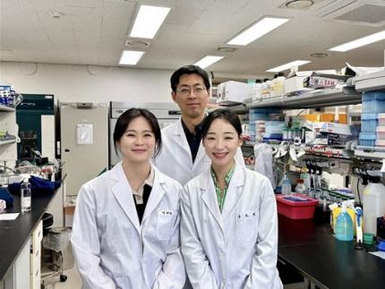
< (From left) Master's candidate Yewon Yang, Professor Yoosik Kim and Ph.D. candidate Doyeong Ku of the Department of Chemical and Biomolecular Engineering >
Autoimmune diseases arise when the immune system fails to differentiate between external pathogens and the body's own molecules, leading to self-directed attacks. Despite extensive research, the precise causes of excessive inflammatory conditions like Sjögren’s syndrome and systemic lupus erythematosus remain unclear, and effective treatments are still limited.
To uncover the molecular mechanisms driving immune hyperactivation and to identify potential regulatory factors, the research team led by Professor Yoosik Kim focused on mitochondrial double-stranded RNA (mt-dsRNA), a genetic immunogenic material produced within cellular organelles. Since mt-dsRNA structurally resembles viral RNA, it can mistakenly trigger immune responses even in the absence of an actual viral infection.
The team discovered that SLIRP, a key regulator of mt-dsRNA, amplifies immune responses by stabilizing the RNA. They confirmed that SLIRP expression increases in experimental models simulating the tissues of autoimmune disease patients and viral infections. Conversely, suppressing SLIRP significantly reduced the immune response, underscoring its role as a critical factor in immune amplification.
This study also demonstrated the dual function of SLIRP in different contexts. In cells infected with human beta coronavirus OC43 and encephalomyocarditis virus (EMCV), SLIRP suppression led to reduced antiviral responses and increased viral replication. Meanwhile, in the blood and salivary gland cells of Sjögren’s syndrome patients, where both SLIRP and mt-dsRNA levels were elevated, suppressing SLIRP alleviated the abnormal immune response.
These findings highlight SLIRP as a key molecular switch that regulates immune responses in both infections and autoimmune diseases.
< Figure 1. Schematic diagram of antiviral signal amplification by SLIRP: SLIRP-based mt-dsRNA induction, cytoplasmic accumulation, and strong interferon response induction by positive feedback of immune response activation. Confirmation of the immune regulatory function of SLIRP in defense against autoimmune diseases Sjögren's syndrome, coronavirus, and encephalomyocarditis virus infection. >
Professor Yoosik Kim remarked, "Through this study, we have identified SLIRP as a crucial protein that drives immune amplification via mt-dsRNAs. Given its dual role in autoimmune diseases and viral infections, SLIRP presents a promising target for immune regulation therapies across various inflammatory disease contexts."
The study, with Ph.D. student Do-Young Ku (first author) and M.S. student Ye-Won Yang (second author) from the Department of Chemical and Biomolecular Engineering at KAIST as primary contributors, was published online in the journal Cell Reports on April 19, 2025.
※ Paper title: SLIRP amplifies antiviral signaling via positive feedback regulation and contributes to autoimmune diseases※ Main authors: Do-Young Ku (KAIST, first author), Ye-Won Yang (KAIST, second author), Seunghee Cha (University of Florida, corresponding author), Yoosik Kim (KAIST, corresponding author)
This study was supported by the Ministry of Health and Welfare's Public Health Technology Research Program and the National Institutes of Health (NIH) through Research Project (R01) funding.
2025.05.14 View 458
KAIST Discovers Protein Switch that Turns Anti-Viral Immune Response On and Off
Even after the COVID-19 pandemic, various new infectious diseases continue to emerge, posing ongoing viral threats that demand robust and sustained immune defenses. However, excessive immune reactions can also harm body tissues, causing significant health issues. KAIST and an international research team have discovered a critical protein that acts as a 'switch' regulating immune responses to viruses. This breakthrough is expected to lay the groundwork for future infectious disease responses and autoimmune disease treatment strategies.
KAIST (President Kwang-Hyung Lee) announced on May 14 that a joint research team led by Professor Yoosik Kim from the Department of Chemical and Biomolecular Engineering at KAIST and Professor Seunghee Cha from University of Florida has discovered the mechanism by which double-stranded RNA derived from mitochondria amplifies immune responses. They identified the protein SLIRP as an 'immune switch' that regulates this process, playing a crucial role in both viral infections and autoimmune diseases.
< (From left) Master's candidate Yewon Yang, Professor Yoosik Kim and Ph.D. candidate Doyeong Ku of the Department of Chemical and Biomolecular Engineering >
Autoimmune diseases arise when the immune system fails to differentiate between external pathogens and the body's own molecules, leading to self-directed attacks. Despite extensive research, the precise causes of excessive inflammatory conditions like Sjögren’s syndrome and systemic lupus erythematosus remain unclear, and effective treatments are still limited.
To uncover the molecular mechanisms driving immune hyperactivation and to identify potential regulatory factors, the research team led by Professor Yoosik Kim focused on mitochondrial double-stranded RNA (mt-dsRNA), a genetic immunogenic material produced within cellular organelles. Since mt-dsRNA structurally resembles viral RNA, it can mistakenly trigger immune responses even in the absence of an actual viral infection.
The team discovered that SLIRP, a key regulator of mt-dsRNA, amplifies immune responses by stabilizing the RNA. They confirmed that SLIRP expression increases in experimental models simulating the tissues of autoimmune disease patients and viral infections. Conversely, suppressing SLIRP significantly reduced the immune response, underscoring its role as a critical factor in immune amplification.
This study also demonstrated the dual function of SLIRP in different contexts. In cells infected with human beta coronavirus OC43 and encephalomyocarditis virus (EMCV), SLIRP suppression led to reduced antiviral responses and increased viral replication. Meanwhile, in the blood and salivary gland cells of Sjögren’s syndrome patients, where both SLIRP and mt-dsRNA levels were elevated, suppressing SLIRP alleviated the abnormal immune response.
These findings highlight SLIRP as a key molecular switch that regulates immune responses in both infections and autoimmune diseases.
< Figure 1. Schematic diagram of antiviral signal amplification by SLIRP: SLIRP-based mt-dsRNA induction, cytoplasmic accumulation, and strong interferon response induction by positive feedback of immune response activation. Confirmation of the immune regulatory function of SLIRP in defense against autoimmune diseases Sjögren's syndrome, coronavirus, and encephalomyocarditis virus infection. >
Professor Yoosik Kim remarked, "Through this study, we have identified SLIRP as a crucial protein that drives immune amplification via mt-dsRNAs. Given its dual role in autoimmune diseases and viral infections, SLIRP presents a promising target for immune regulation therapies across various inflammatory disease contexts."
The study, with Ph.D. student Do-Young Ku (first author) and M.S. student Ye-Won Yang (second author) from the Department of Chemical and Biomolecular Engineering at KAIST as primary contributors, was published online in the journal Cell Reports on April 19, 2025.
※ Paper title: SLIRP amplifies antiviral signaling via positive feedback regulation and contributes to autoimmune diseases※ Main authors: Do-Young Ku (KAIST, first author), Ye-Won Yang (KAIST, second author), Seunghee Cha (University of Florida, corresponding author), Yoosik Kim (KAIST, corresponding author)
This study was supported by the Ministry of Health and Welfare's Public Health Technology Research Program and the National Institutes of Health (NIH) through Research Project (R01) funding.
2025.05.14 View 458 -
 A KAIST Team Develops Face-Conforming LED Mask Showing 340% Improved Efficacy in Deep Skin Elasticity
- A KAIST research team led by Professor Keon Jae Lee has developed a deep skin-stimulating LED mask which has been verified in clinical trials to improve dermis elasticity by 340%.
< Figure 1. Overall concept of face-fit surface-lighting micro-LEDs (FSLED) mask. a. Optical image of the FSLED mask showing uniform surface-lighting. schematic illustration of the FSLED mask. The 2D to 3D transformation procedure b. Difference in cosmetic effect on deep skin elasticity, wrinkles, and sagging between FSLED mask and CLED mask. (improvement percentage in eight weeks) >
Conventional LED masks, with their rigid design, fail to conform closely to the skin's contours. This limitation causes substantial light reflection, with up to 90% reflected over a distance of 2 cm, reducing light penetration and limiting stimulation of the deep skin layers essential for effective skin rejuvenation.
To address these challenges, Professor Lee's team developed a face-conforming surface lighting micro-LED (FSLED) mask, which can provide uniform photostimulation to the dermis. The key technology lies in the mask's ability to deliver uniform light to deep skin tissues while maintaining a conformal skin attachment. This is achieved through a 3D origami structure, integrated with 3,770 micro-LEDs and flexible surface light-diffusion layer, minimizing the gaps between the light source and the skin.
In clinical trials involving 33 participants, the FSLED mask demonstrated a 340% improvement in deep skin elasticity compared to conventional LED masks, proving its efficacy in significantly reducing skin wrinkles, sagging and aging.
Professor Keon Jae Lee said, “The FSLED mask provides cosmetic benefits to the entire facial dermis without the side effects of low-temperature burns, making home-care anti-aging treatment that enhances the quality of human life possible. The product is being manufactured by Fronics, KAIST startup company, and will be distributed globally through Amorepacific's network, with sales starting in November.”
This result titled “Clinical Validation of Face-fit Surface-lighting Micro Light-emitting Diode Mask for Skin Anti-aging Treatment”, in which Min Seo Kim, a student of the Master-Doctorate integrated program, and Jaehun An, a Ph.D. candidate, in the Department of Materials Science and Engineering of KAIST, took part as co-first authors, was published in Advanced Materials on October 22nd, 2024 (DOI: 10.1002/adma.202411651).
Introductory Video: Face-conforming surface LED mask for skin anti-aging ( https://www.youtube.com/watch?v=kSccLwx8N_w )
2024.10.29 View 5247
A KAIST Team Develops Face-Conforming LED Mask Showing 340% Improved Efficacy in Deep Skin Elasticity
- A KAIST research team led by Professor Keon Jae Lee has developed a deep skin-stimulating LED mask which has been verified in clinical trials to improve dermis elasticity by 340%.
< Figure 1. Overall concept of face-fit surface-lighting micro-LEDs (FSLED) mask. a. Optical image of the FSLED mask showing uniform surface-lighting. schematic illustration of the FSLED mask. The 2D to 3D transformation procedure b. Difference in cosmetic effect on deep skin elasticity, wrinkles, and sagging between FSLED mask and CLED mask. (improvement percentage in eight weeks) >
Conventional LED masks, with their rigid design, fail to conform closely to the skin's contours. This limitation causes substantial light reflection, with up to 90% reflected over a distance of 2 cm, reducing light penetration and limiting stimulation of the deep skin layers essential for effective skin rejuvenation.
To address these challenges, Professor Lee's team developed a face-conforming surface lighting micro-LED (FSLED) mask, which can provide uniform photostimulation to the dermis. The key technology lies in the mask's ability to deliver uniform light to deep skin tissues while maintaining a conformal skin attachment. This is achieved through a 3D origami structure, integrated with 3,770 micro-LEDs and flexible surface light-diffusion layer, minimizing the gaps between the light source and the skin.
In clinical trials involving 33 participants, the FSLED mask demonstrated a 340% improvement in deep skin elasticity compared to conventional LED masks, proving its efficacy in significantly reducing skin wrinkles, sagging and aging.
Professor Keon Jae Lee said, “The FSLED mask provides cosmetic benefits to the entire facial dermis without the side effects of low-temperature burns, making home-care anti-aging treatment that enhances the quality of human life possible. The product is being manufactured by Fronics, KAIST startup company, and will be distributed globally through Amorepacific's network, with sales starting in November.”
This result titled “Clinical Validation of Face-fit Surface-lighting Micro Light-emitting Diode Mask for Skin Anti-aging Treatment”, in which Min Seo Kim, a student of the Master-Doctorate integrated program, and Jaehun An, a Ph.D. candidate, in the Department of Materials Science and Engineering of KAIST, took part as co-first authors, was published in Advanced Materials on October 22nd, 2024 (DOI: 10.1002/adma.202411651).
Introductory Video: Face-conforming surface LED mask for skin anti-aging ( https://www.youtube.com/watch?v=kSccLwx8N_w )
2024.10.29 View 5247 -
 Professor Jimin Park and Dr. Inho Kim join the ranks of the 2024 "35 Innovators Under 35" by the MIT Technology Review
< (From left) Professor Jimin Park of the Department of Chemical and Biomolecular Engineering and Dr. Inho Kim, a graduate of the Department of Materials Science and Engineering >
KAIST (represented by President Kwang-Hyung Lee) announced on the 13th of September that Professor Jimin Park from KAIST’s Department of Chemical and Biomolecular Engineering and Dr. Inho Kim, a graduate from the Department of Materials Science and Engineering (currently a postdoctoral researcher at Caltech), were selected by the MIT Technology Review as the 2024 "35 Innovators Under 35”.
The MIT Technology Review, first published in 1899 by the Massachusetts Institute of Technology, is the world’s oldest and most influential magazine on science and technology, offering in-depth analysis across various technology fields, expanding knowledge and providing insights into cutting-edge technology trends.
Since 1999, the magazine has annually named 35 innovators under the age of 35, recognizing young talents making groundbreaking contributions in modern technology fields. The recognition is globally considered a prestigious honor and a dream for young researchers in the science and technology community.
< Image 1. Introduction for Professor Jimin Park at the Meet 35 Innovators Under 35 Summit 2024 >
Professor Jimin Park is developing next-generation bio-interfaces that link artificial materials with living organisms, and is engaged in advanced research in areas such as digital healthcare and carbon-neutral compound manufacturing technologies. In 2014, Professor Park was also recognized as one of the ‘Asia Pacific Innovators Under 35’ by the MIT Technology Review, which highlights young scientists in the Asia-Pacific region.
Professor Park responded, “It’s a great honor to be named as one of the young innovators by the MIT Technology Review, a symbol of innovation with a long history. I will continue to pursue challenging, interdisciplinary research to develop next-generation interfaces that seamlessly connect artificial materials and living organisms, from atomic to system levels.”
< Image 2. Introduction for Dr. Inho Kim as the 2024 Innovator of Materials Science for 35 Innovators Under 35 >
Dr. Inho Kim, who earned his PhD from KAIST in 2020 under the supervision of Professor Sang Ouk Kim from the Department of Materials Science and Engineering, recently succeeded in developing a new artificial muscle using composite fibers. This new material is considered the most human-like muscle ever reported in scientific literature, while also being 17 times stronger than natural human muscle.
Dr. Kim is researching the application of artificial muscle fibers in next-generation wearable assistive devices that move more naturally, like humans or animals, noting that the fibers are lightweight, flexible, and exhibit conductivity during contraction, enabling real-time feedback. Recognized for this potential, Dr. Inho Kim was named one of the '35 Innovators Under 35' this year, making him the first researcher to win the honor with the research conducted at KAIST and a PhD earned from Korea.
Dr. Kim stated, “I aim to develop robots using these new materials that can replace today’s expensive and heavy exoskeleton suits by eliminating motors and rigid frames. This will significantly reduce costs and allow for better customization, making cutting-edge technology more accessible to those who need it most, like children with cerebral palsy.”
2024.09.13 View 5462
Professor Jimin Park and Dr. Inho Kim join the ranks of the 2024 "35 Innovators Under 35" by the MIT Technology Review
< (From left) Professor Jimin Park of the Department of Chemical and Biomolecular Engineering and Dr. Inho Kim, a graduate of the Department of Materials Science and Engineering >
KAIST (represented by President Kwang-Hyung Lee) announced on the 13th of September that Professor Jimin Park from KAIST’s Department of Chemical and Biomolecular Engineering and Dr. Inho Kim, a graduate from the Department of Materials Science and Engineering (currently a postdoctoral researcher at Caltech), were selected by the MIT Technology Review as the 2024 "35 Innovators Under 35”.
The MIT Technology Review, first published in 1899 by the Massachusetts Institute of Technology, is the world’s oldest and most influential magazine on science and technology, offering in-depth analysis across various technology fields, expanding knowledge and providing insights into cutting-edge technology trends.
Since 1999, the magazine has annually named 35 innovators under the age of 35, recognizing young talents making groundbreaking contributions in modern technology fields. The recognition is globally considered a prestigious honor and a dream for young researchers in the science and technology community.
< Image 1. Introduction for Professor Jimin Park at the Meet 35 Innovators Under 35 Summit 2024 >
Professor Jimin Park is developing next-generation bio-interfaces that link artificial materials with living organisms, and is engaged in advanced research in areas such as digital healthcare and carbon-neutral compound manufacturing technologies. In 2014, Professor Park was also recognized as one of the ‘Asia Pacific Innovators Under 35’ by the MIT Technology Review, which highlights young scientists in the Asia-Pacific region.
Professor Park responded, “It’s a great honor to be named as one of the young innovators by the MIT Technology Review, a symbol of innovation with a long history. I will continue to pursue challenging, interdisciplinary research to develop next-generation interfaces that seamlessly connect artificial materials and living organisms, from atomic to system levels.”
< Image 2. Introduction for Dr. Inho Kim as the 2024 Innovator of Materials Science for 35 Innovators Under 35 >
Dr. Inho Kim, who earned his PhD from KAIST in 2020 under the supervision of Professor Sang Ouk Kim from the Department of Materials Science and Engineering, recently succeeded in developing a new artificial muscle using composite fibers. This new material is considered the most human-like muscle ever reported in scientific literature, while also being 17 times stronger than natural human muscle.
Dr. Kim is researching the application of artificial muscle fibers in next-generation wearable assistive devices that move more naturally, like humans or animals, noting that the fibers are lightweight, flexible, and exhibit conductivity during contraction, enabling real-time feedback. Recognized for this potential, Dr. Inho Kim was named one of the '35 Innovators Under 35' this year, making him the first researcher to win the honor with the research conducted at KAIST and a PhD earned from Korea.
Dr. Kim stated, “I aim to develop robots using these new materials that can replace today’s expensive and heavy exoskeleton suits by eliminating motors and rigid frames. This will significantly reduce costs and allow for better customization, making cutting-edge technology more accessible to those who need it most, like children with cerebral palsy.”
2024.09.13 View 5462 -
 Unraveling Mitochondrial DNA Mutations in Human Cells
Throughout our lifetime, cells accumulate DNA mutations, which contribute to genetic diversity, or “mosaicism”, among cells. These genomic mutations are pivotal for the aging process and the onset of various diseases, including cancer. Mitochondria, essential cellular organelles involved in energy metabolism and apoptosis, possess their own DNA, which are susceptible to mutations. However, studies on mtDNA mutations and mosaicism have been limited due to a variety of technical challenges.
Genomic scientists from KAIST have revealed the genetic mosaicism characterized by variations in mitochondrial DNA (mtDNA) across normal human cells. This study provides fundamental insights into understanding human aging and disease onset mechanisms.
The study, “Mitochondrial DNA mosaicism in normal human somatic cells,” was published in Nature Genetics on July 22. It was led by graduate student Jisong An under the supervision of Professor Young Seok Ju from the Graduate School of Medical Science and Engineering.
Researchers from Seoul National University College of Medicine, Yonsei University College of Medicine, Korea University College of Medicine, Washington University School of Medicine National Cancer Center, Seoul National University Hospital, Gangnam Severance Hospital and KAIST faculty startup company Inocras Inc. also participated in this study.
< Figure 1. a. Flow of experiment. b. Schematic diagram illustrating the origin and dynamics of mtDNA alterations across a lifetime. >
The study involved a bioinformatic analysis of whole-genome sequences from 2,096 single cells obtained from normal human colorectal epithelial tissue, fibroblasts, and blood collected from 31 individuals. The study highlights an average of three significant mtDNA differences between cells, with approximately 6% of these variations confirmed to be inherited as heteroplasmy from the mother.
Moreover, mutations significantly increased during tumorigenesis, with some mutations contributing to instability in mitochondrial RNA. Based on these findings, the study illustrates a computational model that comprehensively elucidates the evolution of mitochondria from embryonic development to aging and tumorigenesis.
This study systematically reveals the mechanisms behind mitochondrial DNA mosaicism in normal human cells, establishing a crucial foundation for understanding the impact of mtDNA on aging and disease onset.
Professor Ju remarked, “By systematically utilizing whole-genome big data, we can illuminate previously unknown phenomena in life sciences.” He emphasized the significance of the study, adding, “For the first time, we have established a method to systematically understand mitochondrial DNA changes occurring during human embryonic development, aging, and cancer development.”
This work was supported by the National Research Foundation of Korea and the Suh Kyungbae Foundation.
2024.07.24 View 4193
Unraveling Mitochondrial DNA Mutations in Human Cells
Throughout our lifetime, cells accumulate DNA mutations, which contribute to genetic diversity, or “mosaicism”, among cells. These genomic mutations are pivotal for the aging process and the onset of various diseases, including cancer. Mitochondria, essential cellular organelles involved in energy metabolism and apoptosis, possess their own DNA, which are susceptible to mutations. However, studies on mtDNA mutations and mosaicism have been limited due to a variety of technical challenges.
Genomic scientists from KAIST have revealed the genetic mosaicism characterized by variations in mitochondrial DNA (mtDNA) across normal human cells. This study provides fundamental insights into understanding human aging and disease onset mechanisms.
The study, “Mitochondrial DNA mosaicism in normal human somatic cells,” was published in Nature Genetics on July 22. It was led by graduate student Jisong An under the supervision of Professor Young Seok Ju from the Graduate School of Medical Science and Engineering.
Researchers from Seoul National University College of Medicine, Yonsei University College of Medicine, Korea University College of Medicine, Washington University School of Medicine National Cancer Center, Seoul National University Hospital, Gangnam Severance Hospital and KAIST faculty startup company Inocras Inc. also participated in this study.
< Figure 1. a. Flow of experiment. b. Schematic diagram illustrating the origin and dynamics of mtDNA alterations across a lifetime. >
The study involved a bioinformatic analysis of whole-genome sequences from 2,096 single cells obtained from normal human colorectal epithelial tissue, fibroblasts, and blood collected from 31 individuals. The study highlights an average of three significant mtDNA differences between cells, with approximately 6% of these variations confirmed to be inherited as heteroplasmy from the mother.
Moreover, mutations significantly increased during tumorigenesis, with some mutations contributing to instability in mitochondrial RNA. Based on these findings, the study illustrates a computational model that comprehensively elucidates the evolution of mitochondria from embryonic development to aging and tumorigenesis.
This study systematically reveals the mechanisms behind mitochondrial DNA mosaicism in normal human cells, establishing a crucial foundation for understanding the impact of mtDNA on aging and disease onset.
Professor Ju remarked, “By systematically utilizing whole-genome big data, we can illuminate previously unknown phenomena in life sciences.” He emphasized the significance of the study, adding, “For the first time, we have established a method to systematically understand mitochondrial DNA changes occurring during human embryonic development, aging, and cancer development.”
This work was supported by the National Research Foundation of Korea and the Suh Kyungbae Foundation.
2024.07.24 View 4193 -
 KAIST researchers devises a technology to utilize ultrahigh-resolution micro-LED with 40% reduced self-generated heat
In the digitized modern life, various forms of future displays, such as wearable and rollable displays are required. More and more people are wanting to connect to the virtual world whenever and wherever with the use of their smartglasses or smartwatches. Even further, we’ve been hearing about medical diagnosis kit on a shirt and a theatre-hat. However, it is not quite here in our hands yet due to technical limitations of being unable to fit as many pixels as a limited surface area of a glasses while keeping the power consumption at the a level that a hand held battery can supply, all the while the resolution of 4K+ is needed in order to perfectly immerse the users into the augmented or virtual reality through a wireless smartglasses or whatever the device.
KAIST (President Kwang Hyung Lee) announced on the 22nd that Professor Sang Hyeon Kim's research team of the Department of Electrical and Electronic Engineering re-examined the phenomenon of efficiency degradation of micro-LEDs with pixels in a size of micrometers (μm, one millionth of a meter) and found that it was possible to fundamentally resolve the problem by the use of epitaxial structure engineering.
Epitaxy refers to the process of stacking gallium nitride crystals that are used as a light emitting body on top of an ultrapure silicon or sapphire substrate used for μLEDs as a medium.
μLED is being actively studied because it has the advantages of superior brightness, contrast ratio, and lifespan compared to OLED. In 2018, Samsung Electronics commercialized a product equipped with μLED called 'The Wall'. And there is a prospect that Apple may be launching a μLED-mounted product in 2025.
In order to manufacture μLEDs, pixels are formed by cutting the epitaxial structure grown on a wafer into a cylinder or cuboid shape through an etching process, and this etching process is accompanied by a plasma-based process. However, these plasmas generate defects on the side of the pixel during the pixel formation process.
Therefore, as the pixel size becomes smaller and the resolution increases, the ratio of the surface area to the volume of the pixel increases, and defects on the side of the device that occur during processing further reduce the device efficiency of the μLED. Accordingly, a considerable amount of research has been conducted on mitigating or removing sidewall defects, but this method has a limit to the degree of improvement as it must be done at the post-processing stage after the grown of the epitaxial structure is finished.
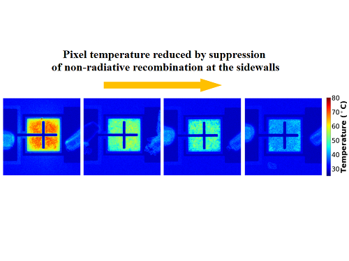
The research team identified that there is a difference in the current moving to the sidewall of the μLED depending on the epitaxial structure during μLED device operation, and based on the findings, the team built a structure that is not sensitive to sidewall defects to solve the problem of reduced efficiency due to miniaturization of μLED devices. In addition, the proposed structure reduced the self-generated heat while the device was running by about 40% compared to the existing structure, which is also of great significance in commercialization of ultrahigh-resolution μLED displays.
This study, which was led by Woo Jin Baek of Professor Sang Hyeon Kim's research team at the KAIST School of Electrical and Electronic Engineering as the first author with guidance by Professor Sang Hyeon Kim and Professor Dae-Myeong Geum of the Chungbuk National University (who was with the team as a postdoctoral researcher at the time) as corresponding authors, was published in the international journal, 'Nature Communications' on March 17th. (Title of the paper: Ultra-low-current driven InGaN blue micro light-emitting diodes for electrically efficient and self-heating relaxed microdisplay).
Professor Sang Hyeon Kim said, "This technological development has great meaning in identifying the cause of the drop in efficiency, which was an obstacle to miniaturization of μLED, and solving it with the design of the epitaxial structure.“ He added, ”We are looking forward to it being used in manufacturing of ultrahigh-resolution displays in the future."
This research was carried out with the support of the Samsung Future Technology Incubation Center.
Figure 1. Image of electroluminescence distribution of μLEDs fabricated from epitaxial structures with quantum barriers of different thicknesses while the current is running
Figure 2. Thermal distribution images of devices fabricated with different epitaxial structures under the same amount of light.
Figure 3. Normalized external quantum efficiency of the device fabricated with the optimized epitaxial structure by sizes.
2023.03.23 View 6797
KAIST researchers devises a technology to utilize ultrahigh-resolution micro-LED with 40% reduced self-generated heat
In the digitized modern life, various forms of future displays, such as wearable and rollable displays are required. More and more people are wanting to connect to the virtual world whenever and wherever with the use of their smartglasses or smartwatches. Even further, we’ve been hearing about medical diagnosis kit on a shirt and a theatre-hat. However, it is not quite here in our hands yet due to technical limitations of being unable to fit as many pixels as a limited surface area of a glasses while keeping the power consumption at the a level that a hand held battery can supply, all the while the resolution of 4K+ is needed in order to perfectly immerse the users into the augmented or virtual reality through a wireless smartglasses or whatever the device.
KAIST (President Kwang Hyung Lee) announced on the 22nd that Professor Sang Hyeon Kim's research team of the Department of Electrical and Electronic Engineering re-examined the phenomenon of efficiency degradation of micro-LEDs with pixels in a size of micrometers (μm, one millionth of a meter) and found that it was possible to fundamentally resolve the problem by the use of epitaxial structure engineering.
Epitaxy refers to the process of stacking gallium nitride crystals that are used as a light emitting body on top of an ultrapure silicon or sapphire substrate used for μLEDs as a medium.
μLED is being actively studied because it has the advantages of superior brightness, contrast ratio, and lifespan compared to OLED. In 2018, Samsung Electronics commercialized a product equipped with μLED called 'The Wall'. And there is a prospect that Apple may be launching a μLED-mounted product in 2025.
In order to manufacture μLEDs, pixels are formed by cutting the epitaxial structure grown on a wafer into a cylinder or cuboid shape through an etching process, and this etching process is accompanied by a plasma-based process. However, these plasmas generate defects on the side of the pixel during the pixel formation process.
Therefore, as the pixel size becomes smaller and the resolution increases, the ratio of the surface area to the volume of the pixel increases, and defects on the side of the device that occur during processing further reduce the device efficiency of the μLED. Accordingly, a considerable amount of research has been conducted on mitigating or removing sidewall defects, but this method has a limit to the degree of improvement as it must be done at the post-processing stage after the grown of the epitaxial structure is finished.
The research team identified that there is a difference in the current moving to the sidewall of the μLED depending on the epitaxial structure during μLED device operation, and based on the findings, the team built a structure that is not sensitive to sidewall defects to solve the problem of reduced efficiency due to miniaturization of μLED devices. In addition, the proposed structure reduced the self-generated heat while the device was running by about 40% compared to the existing structure, which is also of great significance in commercialization of ultrahigh-resolution μLED displays.
This study, which was led by Woo Jin Baek of Professor Sang Hyeon Kim's research team at the KAIST School of Electrical and Electronic Engineering as the first author with guidance by Professor Sang Hyeon Kim and Professor Dae-Myeong Geum of the Chungbuk National University (who was with the team as a postdoctoral researcher at the time) as corresponding authors, was published in the international journal, 'Nature Communications' on March 17th. (Title of the paper: Ultra-low-current driven InGaN blue micro light-emitting diodes for electrically efficient and self-heating relaxed microdisplay).
Professor Sang Hyeon Kim said, "This technological development has great meaning in identifying the cause of the drop in efficiency, which was an obstacle to miniaturization of μLED, and solving it with the design of the epitaxial structure.“ He added, ”We are looking forward to it being used in manufacturing of ultrahigh-resolution displays in the future."
This research was carried out with the support of the Samsung Future Technology Incubation Center.
Figure 1. Image of electroluminescence distribution of μLEDs fabricated from epitaxial structures with quantum barriers of different thicknesses while the current is running
Figure 2. Thermal distribution images of devices fabricated with different epitaxial structures under the same amount of light.
Figure 3. Normalized external quantum efficiency of the device fabricated with the optimized epitaxial structure by sizes.
2023.03.23 View 6797 -
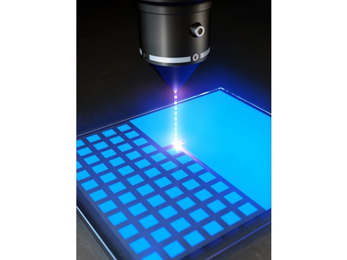 KAIST researchers develops a tech to enable production of ultrahigh-resolution LED with sub-micrometer scale pixels
Ultrahigh-resolution displays are an essential element for developing next-generation electronic products such as virtual reality (VR), augmented reality (AR), and smart watches, and can be applied not only to head-mounted displays, but also to smart glasses and smart lenses. The technology developed through this research is expected to be used to make such next-generation ultrahigh-resolution displays and other various sub-micro optoelectronic devices.
KAIST (President Kwang Hyung Lee) announced on the 22nd that Professor Yong-Hoon Cho's research team of KAIST Department of Physics developed the core technology for an ultrahigh resolution light-emitting diode (LED) display that can realize 0.5 micron-scale pixels smaller than 1/100 of the average hair thickness (about 100 microns) using focused ion beams.
Commonly, pixelation of ultrahigh-resolution LED displays usually relies on the etching method that physically cuts the area around the pixel, but as the pixel becomes smaller due to the occurrence of various defects around it, leading to side-effects of having leakage of current increased and light-emission efficiency decreased. In addition, various complex processes such as patterning for pixelation and post-processing for prevention of leakage current are required.
Professor Yong-Hoon Cho's research team developed a technology that can create pixels down to the size of a microscale without the complicated pre- and post-processing using a focused ion beam. This method has the advantage of being able to freely set the shape of the emitting pixel without causing any structural deformation on the material surface by controlling the intensity of the focused ion beam.
The focused ion beam technology has been widely used for ultrahigh-magnification imaging and nanostructure fabrication in fields such as materials engineering and biology. However, when a focused ion beam is used on a light emitting body such as an LED, light emission of a portion hit by the beam and a surrounding area rapidly decreases, which has been a barrier to fabricating a nano-scale light emitting structure. Upon facing this issue, Professor Cho's research team began the research on the idea that if they turned things around to use these problematic phenomena, they can be used in ultra-fine pixelation method on a sub-micron scale.
The research team used a focused ion beam whose intensity was softened to the extent that the surface was not shaved, and found that not only the light-emission rapidly decreased in the area hit by the focused ion beam, but also the local resistance greatly increased. As a result, while the surface of the LED is kept flat, the portion hit by the focused ion beam is optically and electrically isolated, enabling pixelation for independent operation.
Professor Yong-Hoon Cho, who led the research, said, “We have newly developed a technology that can create sub-micron-scale pixels without complicated processes using a focused ion beam, which will be a base technology that can be applied to next-generation ultrahigh-resolution displays and nano-photoelectronic devices.”
This research in which the Master's student Ji-Hwan Moon and the Ph.D. student Baul Kim of KAIST Department of Physics participated as co-first authors, was carried out with the support of the National Research Foundation of Korea's Support Program for Mid-Career Researchers and the Institute of Information and Communications Technology Planning and Evaluation. It was published online in 'Advanced Materials' on February 13, and was also selected as the internal cover of the next offline edition. (Title: Electrically Driven Sub-Micron Light-Emitting Diode Arrays Using Maskless and Etching-Free Pixelation)
Figure 1. Schematic diagram of the technology for ultrahigh density sub-micron-sized pixels through He focused ion beam (FIB) irradiation on an LED device
Figure 2. Ultra-high-density pixelation technology of micro light-emitting diodes (μLED) through He focused ion beam (FIB) irradiation
Figure 3. Rectangular pixels of different sizes (surface structure picture and luminescence picture) realized by a focused ion beam. Luminescence pictures of pixel arrays ranging in size from 20 µm x 20 µm to 0.5 µm x 0.5 µm, with surface flatness maintained.
2023.03.08 View 7312
KAIST researchers develops a tech to enable production of ultrahigh-resolution LED with sub-micrometer scale pixels
Ultrahigh-resolution displays are an essential element for developing next-generation electronic products such as virtual reality (VR), augmented reality (AR), and smart watches, and can be applied not only to head-mounted displays, but also to smart glasses and smart lenses. The technology developed through this research is expected to be used to make such next-generation ultrahigh-resolution displays and other various sub-micro optoelectronic devices.
KAIST (President Kwang Hyung Lee) announced on the 22nd that Professor Yong-Hoon Cho's research team of KAIST Department of Physics developed the core technology for an ultrahigh resolution light-emitting diode (LED) display that can realize 0.5 micron-scale pixels smaller than 1/100 of the average hair thickness (about 100 microns) using focused ion beams.
Commonly, pixelation of ultrahigh-resolution LED displays usually relies on the etching method that physically cuts the area around the pixel, but as the pixel becomes smaller due to the occurrence of various defects around it, leading to side-effects of having leakage of current increased and light-emission efficiency decreased. In addition, various complex processes such as patterning for pixelation and post-processing for prevention of leakage current are required.
Professor Yong-Hoon Cho's research team developed a technology that can create pixels down to the size of a microscale without the complicated pre- and post-processing using a focused ion beam. This method has the advantage of being able to freely set the shape of the emitting pixel without causing any structural deformation on the material surface by controlling the intensity of the focused ion beam.
The focused ion beam technology has been widely used for ultrahigh-magnification imaging and nanostructure fabrication in fields such as materials engineering and biology. However, when a focused ion beam is used on a light emitting body such as an LED, light emission of a portion hit by the beam and a surrounding area rapidly decreases, which has been a barrier to fabricating a nano-scale light emitting structure. Upon facing this issue, Professor Cho's research team began the research on the idea that if they turned things around to use these problematic phenomena, they can be used in ultra-fine pixelation method on a sub-micron scale.
The research team used a focused ion beam whose intensity was softened to the extent that the surface was not shaved, and found that not only the light-emission rapidly decreased in the area hit by the focused ion beam, but also the local resistance greatly increased. As a result, while the surface of the LED is kept flat, the portion hit by the focused ion beam is optically and electrically isolated, enabling pixelation for independent operation.
Professor Yong-Hoon Cho, who led the research, said, “We have newly developed a technology that can create sub-micron-scale pixels without complicated processes using a focused ion beam, which will be a base technology that can be applied to next-generation ultrahigh-resolution displays and nano-photoelectronic devices.”
This research in which the Master's student Ji-Hwan Moon and the Ph.D. student Baul Kim of KAIST Department of Physics participated as co-first authors, was carried out with the support of the National Research Foundation of Korea's Support Program for Mid-Career Researchers and the Institute of Information and Communications Technology Planning and Evaluation. It was published online in 'Advanced Materials' on February 13, and was also selected as the internal cover of the next offline edition. (Title: Electrically Driven Sub-Micron Light-Emitting Diode Arrays Using Maskless and Etching-Free Pixelation)
Figure 1. Schematic diagram of the technology for ultrahigh density sub-micron-sized pixels through He focused ion beam (FIB) irradiation on an LED device
Figure 2. Ultra-high-density pixelation technology of micro light-emitting diodes (μLED) through He focused ion beam (FIB) irradiation
Figure 3. Rectangular pixels of different sizes (surface structure picture and luminescence picture) realized by a focused ion beam. Luminescence pictures of pixel arrays ranging in size from 20 µm x 20 µm to 0.5 µm x 0.5 µm, with surface flatness maintained.
2023.03.08 View 7312 -
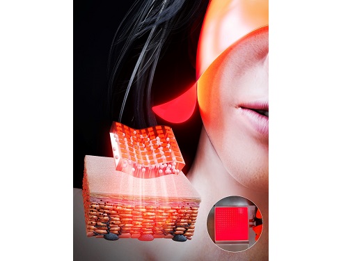 KAIST Team Develops Surface-Lighting MicroLED Patch with Significant Melanogenesis Inhibition Effect
A KAIST research team led by Ph.d candidate Jae Hee Lee and Professor Keon Jae Lee from the Department of Materials Science and Engineering has developed a surface-lighting microLED patch for UV-induced melanogenesis inhibition.
Melanin is brown or dark pigments existing in the skin, which can be abnormally synthesized by external UV or stress. Since the excessive melanin leads to skin diseases such as spots and freckles, proper treatment is required to return normal skin condition.
Recently, LED-based photo-stimulators have been released for skin care, however, their therapeutic effect is still controversial. Since conventional LED stimulators cannot conformally attach to the human skin, distance-induced side effects are caused by light loss and high heat transfer. To achieve effective phototreatment, the LED stimulator needs to be irradiated in contact with the human skin surface, enabling proper and uniform light deliver to the dermis with minimal optical loss.
In this work, the research team fabricated skin-attachable surface-lighting microLED (SµLED, 4 × 4 cm2) patch by utilizing a thousand of microLED chips and silica-embedded light diffusion layer. 100 µm-sized LED chips are vertically-interconnected for high flexibility and low heat generation, allowing its long-term operation on the human skin.
< Image 1. The overall concept of SµLED patch. a) SµLED patch operated on the human skin. b) Schematic illustration of SµLED patch structure. c) 4 × 4 cm2-sized SµLED patch. d) Schematic illustration of the advantages of SµLED patch such as efficient light delivery, low heat generation, and surface-lighting irradiation. >
The research team confirmed melanogenesis inhibition by irradiating the SµLED patch and the conventional LED (CLED) on the artificial human skin and mice dorsal skin. The SµLED-treated groups of human cells and mouse tissues showed minimal epidermal photo-toxicity and consistently effective reduction in synthesized melanin, compared to CLED-treated groups. In addition, significant suppression of proteins/catalysts expression involved in melanin synthesis such as MITF (microphthalmia-associated transcription factor), Melan-A and tyrosinase was verified.
< Image 2. The efficacy of melanogenesis inhibition on 3D human skin cells. a). Different irradiation conditions for a-MSH (major factor to stimulate melanin synthesis) treated cells. b) The ratio of pigmented area to total epidermis area. c) Relative variance of melanin level in 1 cm2-sized skin cells. A low variance means that melanin is evenly distributed, and a high variance means that the melanin is irregularly distributed. d) Optical images after in vitro experiments for 12 days. Scale bar, 1cm. e) Histological analysis of 3D skin, showing the greatest reduction in melanin after SµLED irradiation. Scale bar, 20 µm. >
< Image 3. The efficacy of melanogenesis inhibition on mouse dorsal skin. a) Optical images of mice dorsal skin after photo-treatment for 20 days. b) Histological analysis of mice dorsal skin. Less brown color means less expression of protein/catalysis involved in melanin synthesis. Scale bar, 50 µm. >
Prof. Keon Jae Lee said, “Our inorganic-based SµLED patch has outstanding characteristics in light efficiency, reliability, and durability. The SµLED patch is expected to give a great impact on the cosmetic field by reducing side effects and maximizing phototherapeutic effects.” The core technology of cosmetic SµLED has been transferred to Fronics co., Ltd, founded by Prof. Lee. Fronics is building foundry and equipment for mass production of SµLED masks for whole face cover and plans to release the products in March next year.
This paper entitled “Wearable Surface-Lighting Micro-Light-Emitting Diode Patch for Melanogenesis Inhibition” was published in the November 2022 issue of Advanced Healthcare Materials.
2022.11.22 View 11140
KAIST Team Develops Surface-Lighting MicroLED Patch with Significant Melanogenesis Inhibition Effect
A KAIST research team led by Ph.d candidate Jae Hee Lee and Professor Keon Jae Lee from the Department of Materials Science and Engineering has developed a surface-lighting microLED patch for UV-induced melanogenesis inhibition.
Melanin is brown or dark pigments existing in the skin, which can be abnormally synthesized by external UV or stress. Since the excessive melanin leads to skin diseases such as spots and freckles, proper treatment is required to return normal skin condition.
Recently, LED-based photo-stimulators have been released for skin care, however, their therapeutic effect is still controversial. Since conventional LED stimulators cannot conformally attach to the human skin, distance-induced side effects are caused by light loss and high heat transfer. To achieve effective phototreatment, the LED stimulator needs to be irradiated in contact with the human skin surface, enabling proper and uniform light deliver to the dermis with minimal optical loss.
In this work, the research team fabricated skin-attachable surface-lighting microLED (SµLED, 4 × 4 cm2) patch by utilizing a thousand of microLED chips and silica-embedded light diffusion layer. 100 µm-sized LED chips are vertically-interconnected for high flexibility and low heat generation, allowing its long-term operation on the human skin.
< Image 1. The overall concept of SµLED patch. a) SµLED patch operated on the human skin. b) Schematic illustration of SµLED patch structure. c) 4 × 4 cm2-sized SµLED patch. d) Schematic illustration of the advantages of SµLED patch such as efficient light delivery, low heat generation, and surface-lighting irradiation. >
The research team confirmed melanogenesis inhibition by irradiating the SµLED patch and the conventional LED (CLED) on the artificial human skin and mice dorsal skin. The SµLED-treated groups of human cells and mouse tissues showed minimal epidermal photo-toxicity and consistently effective reduction in synthesized melanin, compared to CLED-treated groups. In addition, significant suppression of proteins/catalysts expression involved in melanin synthesis such as MITF (microphthalmia-associated transcription factor), Melan-A and tyrosinase was verified.
< Image 2. The efficacy of melanogenesis inhibition on 3D human skin cells. a). Different irradiation conditions for a-MSH (major factor to stimulate melanin synthesis) treated cells. b) The ratio of pigmented area to total epidermis area. c) Relative variance of melanin level in 1 cm2-sized skin cells. A low variance means that melanin is evenly distributed, and a high variance means that the melanin is irregularly distributed. d) Optical images after in vitro experiments for 12 days. Scale bar, 1cm. e) Histological analysis of 3D skin, showing the greatest reduction in melanin after SµLED irradiation. Scale bar, 20 µm. >
< Image 3. The efficacy of melanogenesis inhibition on mouse dorsal skin. a) Optical images of mice dorsal skin after photo-treatment for 20 days. b) Histological analysis of mice dorsal skin. Less brown color means less expression of protein/catalysis involved in melanin synthesis. Scale bar, 50 µm. >
Prof. Keon Jae Lee said, “Our inorganic-based SµLED patch has outstanding characteristics in light efficiency, reliability, and durability. The SµLED patch is expected to give a great impact on the cosmetic field by reducing side effects and maximizing phototherapeutic effects.” The core technology of cosmetic SµLED has been transferred to Fronics co., Ltd, founded by Prof. Lee. Fronics is building foundry and equipment for mass production of SµLED masks for whole face cover and plans to release the products in March next year.
This paper entitled “Wearable Surface-Lighting Micro-Light-Emitting Diode Patch for Melanogenesis Inhibition” was published in the November 2022 issue of Advanced Healthcare Materials.
2022.11.22 View 11140 -
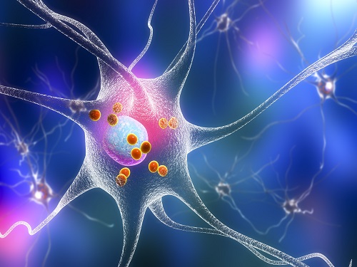 KAIST Research Team Proves How a Neurotransmitter may be the Key in Controlling Alzheimer’s Toxicity
With nearly 50 million dementia patients worldwide, and Alzheimers’s disease is the most common neurodegenerative disease. Its main symptom is the impairment of general cognitive abilities, including the ability to speak or to remember. The importance of finding a cure is widely understood with increasingly aging population and the life expectancy being ever-extended. However, even the cause of the grim disease is yet to be given a clear definition.
A KAIST research team in the Department of Chemistry led by professor Mi Hee Lim took on a lead to discovered a new role for somatostatin, a protein-based neurotransmitter, in reducing the toxicity caused in the pathogenic mechanism taken towards development of Alzheimer’s disease. The study was published in the July issue of Nature Chemistry under the title, “Conformational and functional changes of the native neuropeptide somatostatin occur in the presence of copper and amyloid-β”.
According to the amyloid hypothesis, the abnormal deposition of Aβ proteins causes death of neuronal cells. While Aβ agglomerations make up most of the aged plaques through fibrosis, in recent studies, high concentrations of transitional metal were found in the plaques from Alzheimer’s patients.
This suggests a close interaction between metallic ions and Aβ, which accelerates the fibrosis of proteins. Copper in particular is a redox-activating transition metal that can produce large amounts of oxygen and cause serious oxidative stress on cell organelles. Aβ proteins and transition metals can closely interact with neurotransmitters at synapses, but the direct effects of such abnormalities on the structure and function of neurotransmitters are yet to be understood.
Figure 1. Functional shift of somatostatin (SST) by factors in the pathogenesis of Alzheimer's disease.
Figure 2. Somatostatin’s loss-of-function as neurotransmitter. a. Schematic diagram of SST auto-aggregation due to Alzheimer's pathological factors. b. SST’s aggregation by copper ions. c. Coordination-prediction structure and N-terminal folding of copper-SST. d. Inhibition of SST receptor binding specificity by metals.
In their research, Professor Lim’s team discovered that when somatostatin, the protein-based neurotransmitter, is met with copper, Aβ, and metal-Aβ complexes, self-aggregates and ceases to perform its innate function of transmitting neural signals, but begins to attenuate the toxicity and agglomeration of metal-Aβ complexes.
Figure 3. Gain-of-function of somatostatin (SST) in the dementia setting. a. Prediction of docking of SST and amyloid beta. b. SST making metal-amyloid beta aggregates into an amorphous form. c. Cytotoxic mitigation effect of SST. d. SST mitigating the interaction between amyloid beta protein with the cell membrane.
This research, by Dr. Jiyeon Han et al. from the KAIST Department of Chemistry, revealed the coordination structure between copper and somatostatin at a molecular level through which it suggested the agglomeration mechanism, and discovered the effects of somatostatin on Aβ agglomeration path depending on the presence or absence of metals. The team has further confirmed somatostatin’s receptor binding, interactions with cell membranes, and effects on cell toxicity for the first time to receive international attention.
Professor Mi Hee Lim said, “This research has great significance in having discovered a new role of neurotransmitters in the pathogenesis of Alzheimer’s disease.” “We expect this research to contribute to defining the pathogenic network of neurodegenerative diseases caused by aging, and to the development of future biomarkers and medicine,” she added.
This research was conducted jointly by Professor Seung-Hee Lee’s team of KAIST Department of Biological Sciences, Professor Kiyoung Park’s Team of KAIST Department of Chemistry, and Professor Yulong Li’s team of Peking University.
The research was funded by Basic Science Research Program of the National Research Foundation of Korea and KAIST.
For more information about the research team, visit the website: https://sites.google.com/site/miheelimlab/1-professor-mi-hee-lim.
2022.07.29 View 13847
KAIST Research Team Proves How a Neurotransmitter may be the Key in Controlling Alzheimer’s Toxicity
With nearly 50 million dementia patients worldwide, and Alzheimers’s disease is the most common neurodegenerative disease. Its main symptom is the impairment of general cognitive abilities, including the ability to speak or to remember. The importance of finding a cure is widely understood with increasingly aging population and the life expectancy being ever-extended. However, even the cause of the grim disease is yet to be given a clear definition.
A KAIST research team in the Department of Chemistry led by professor Mi Hee Lim took on a lead to discovered a new role for somatostatin, a protein-based neurotransmitter, in reducing the toxicity caused in the pathogenic mechanism taken towards development of Alzheimer’s disease. The study was published in the July issue of Nature Chemistry under the title, “Conformational and functional changes of the native neuropeptide somatostatin occur in the presence of copper and amyloid-β”.
According to the amyloid hypothesis, the abnormal deposition of Aβ proteins causes death of neuronal cells. While Aβ agglomerations make up most of the aged plaques through fibrosis, in recent studies, high concentrations of transitional metal were found in the plaques from Alzheimer’s patients.
This suggests a close interaction between metallic ions and Aβ, which accelerates the fibrosis of proteins. Copper in particular is a redox-activating transition metal that can produce large amounts of oxygen and cause serious oxidative stress on cell organelles. Aβ proteins and transition metals can closely interact with neurotransmitters at synapses, but the direct effects of such abnormalities on the structure and function of neurotransmitters are yet to be understood.
Figure 1. Functional shift of somatostatin (SST) by factors in the pathogenesis of Alzheimer's disease.
Figure 2. Somatostatin’s loss-of-function as neurotransmitter. a. Schematic diagram of SST auto-aggregation due to Alzheimer's pathological factors. b. SST’s aggregation by copper ions. c. Coordination-prediction structure and N-terminal folding of copper-SST. d. Inhibition of SST receptor binding specificity by metals.
In their research, Professor Lim’s team discovered that when somatostatin, the protein-based neurotransmitter, is met with copper, Aβ, and metal-Aβ complexes, self-aggregates and ceases to perform its innate function of transmitting neural signals, but begins to attenuate the toxicity and agglomeration of metal-Aβ complexes.
Figure 3. Gain-of-function of somatostatin (SST) in the dementia setting. a. Prediction of docking of SST and amyloid beta. b. SST making metal-amyloid beta aggregates into an amorphous form. c. Cytotoxic mitigation effect of SST. d. SST mitigating the interaction between amyloid beta protein with the cell membrane.
This research, by Dr. Jiyeon Han et al. from the KAIST Department of Chemistry, revealed the coordination structure between copper and somatostatin at a molecular level through which it suggested the agglomeration mechanism, and discovered the effects of somatostatin on Aβ agglomeration path depending on the presence or absence of metals. The team has further confirmed somatostatin’s receptor binding, interactions with cell membranes, and effects on cell toxicity for the first time to receive international attention.
Professor Mi Hee Lim said, “This research has great significance in having discovered a new role of neurotransmitters in the pathogenesis of Alzheimer’s disease.” “We expect this research to contribute to defining the pathogenic network of neurodegenerative diseases caused by aging, and to the development of future biomarkers and medicine,” she added.
This research was conducted jointly by Professor Seung-Hee Lee’s team of KAIST Department of Biological Sciences, Professor Kiyoung Park’s Team of KAIST Department of Chemistry, and Professor Yulong Li’s team of Peking University.
The research was funded by Basic Science Research Program of the National Research Foundation of Korea and KAIST.
For more information about the research team, visit the website: https://sites.google.com/site/miheelimlab/1-professor-mi-hee-lim.
2022.07.29 View 13847 -
 The Dynamic Tracking of Tissue-Specific Secretory Proteins
Researchers develop a versatile and powerful tool for studying the spatiotemporal dynamics of secretory proteins, a valuable class of biomarkers and therapeutic targets
Researchers have presented a method for profiling tissue-specific secretory proteins in live mice. This method is expected to be applicable to various tissues or disease models for investigating biomarkers or therapeutic targets involved in disease progression. This research was reported in Nature Communications on September 1.
Secretory proteins released into the blood play essential roles in physiological systems. They are core mediators of interorgan communication, while serving as biomarkers and therapeutic targets.
Previous studies have analyzed conditioned media from culture models to identify cell type-specific secretory proteins, but these models often fail to fully recapitulate the intricacies of multi-organ systems and thus do not sufficiently reflect biological realities.
These limitations provided compelling motivation for the research team led by Jae Myoung Suh and his collaborators to develop techniques that could identify and resolve characteristics of tissue-specific secretory proteins along time and space dimensions.
For addressing this gap in the current methodology, the research team utilized proximity-labeling enzymes such as TurboID to label secretory proteins in endoplasmic reticulum lumen using biotin. Thereafter, the biotin-labeled secretory proteins were readily enriched through streptavidin affinity purification and could be identified through mass spectrometry.
To demonstrate its functionality in live mice, research team delivered TurboID to mouse livers via an adenovirus. After administering the biotin, only liver-derived secretory proteins were successfully detected in the plasma of the mice. Interestingly, the pattern of biotin-labeled proteins secreted from the liver was clearly distinctive from those of hepatocyte cell lines.
First author Kwang-eun Kim from the Graduate School of Medical Science and Engineering explained, “The proteins secreted by the liver were significantly different from the results of cell culture models. This data shows the limitations of cell culture models for secretory protein study, and this technique can overcome those limitations. It can be further used to discover biomarkers and therapeutic targets that can more fully reflect the physiological state.”
This work research was supported by the National Research Foundation of Korea, the KAIST Key Research Institutes Project (Interdisciplinary Research Group), and the Institute for Basic Science in Korea.
-PublicationKwang-eun Kim, Isaac Park et al., “Dynamic tracking and identification of tissue-specific secretory proteins in the circulation of live mice,” Nature Communications on Sept.1,
2021(https://doi.org/10.1038/s41467-021-25546-y)
-ProfileProfessor Jae Myoung Suh Integrated Lab of Metabolism, Obesity and Diabetes Researchhttps://imodkaist.wixsite.com/home
Graduate School of Medical Science and Engineering College of Life Science and BioengineeringKAIST
2021.09.14 View 9454
The Dynamic Tracking of Tissue-Specific Secretory Proteins
Researchers develop a versatile and powerful tool for studying the spatiotemporal dynamics of secretory proteins, a valuable class of biomarkers and therapeutic targets
Researchers have presented a method for profiling tissue-specific secretory proteins in live mice. This method is expected to be applicable to various tissues or disease models for investigating biomarkers or therapeutic targets involved in disease progression. This research was reported in Nature Communications on September 1.
Secretory proteins released into the blood play essential roles in physiological systems. They are core mediators of interorgan communication, while serving as biomarkers and therapeutic targets.
Previous studies have analyzed conditioned media from culture models to identify cell type-specific secretory proteins, but these models often fail to fully recapitulate the intricacies of multi-organ systems and thus do not sufficiently reflect biological realities.
These limitations provided compelling motivation for the research team led by Jae Myoung Suh and his collaborators to develop techniques that could identify and resolve characteristics of tissue-specific secretory proteins along time and space dimensions.
For addressing this gap in the current methodology, the research team utilized proximity-labeling enzymes such as TurboID to label secretory proteins in endoplasmic reticulum lumen using biotin. Thereafter, the biotin-labeled secretory proteins were readily enriched through streptavidin affinity purification and could be identified through mass spectrometry.
To demonstrate its functionality in live mice, research team delivered TurboID to mouse livers via an adenovirus. After administering the biotin, only liver-derived secretory proteins were successfully detected in the plasma of the mice. Interestingly, the pattern of biotin-labeled proteins secreted from the liver was clearly distinctive from those of hepatocyte cell lines.
First author Kwang-eun Kim from the Graduate School of Medical Science and Engineering explained, “The proteins secreted by the liver were significantly different from the results of cell culture models. This data shows the limitations of cell culture models for secretory protein study, and this technique can overcome those limitations. It can be further used to discover biomarkers and therapeutic targets that can more fully reflect the physiological state.”
This work research was supported by the National Research Foundation of Korea, the KAIST Key Research Institutes Project (Interdisciplinary Research Group), and the Institute for Basic Science in Korea.
-PublicationKwang-eun Kim, Isaac Park et al., “Dynamic tracking and identification of tissue-specific secretory proteins in the circulation of live mice,” Nature Communications on Sept.1,
2021(https://doi.org/10.1038/s41467-021-25546-y)
-ProfileProfessor Jae Myoung Suh Integrated Lab of Metabolism, Obesity and Diabetes Researchhttps://imodkaist.wixsite.com/home
Graduate School of Medical Science and Engineering College of Life Science and BioengineeringKAIST
2021.09.14 View 9454 -
 Quantum Emitters: Beyond Crystal Clear to Single-Photon Pure
‘Nanoscale Focus Pinspot’ can quench only the background noise without changing the optical properties of the quantum emitter and the built-in photonic structure
Photons, fundamental particles of light, are carrying these words to your eyes via the light from your computer screen or phone. Photons play a key role in the next-generation quantum information technology, such as quantum computing and communications. A quantum emitter, capable of producing a single, pure photon, is the crux of such technology but has many issues that have yet to be solved, according to KAIST researchers.
A research team under Professor Yong-Hoon Cho has developed a technique that can isolate the desired quality emitter by reducing the noise surrounding the target with what they have dubbed a ‘nanoscale focus pinspot.’ They published their results on June 24 in ACS Nano.
“The nanoscale focus pinspot is a structurally nondestructive technique under an extremely low dose ion beam and is generally applicable for various platforms to improve their single-photon purity while retaining the integrated photonic structures,” said lead author Yong-Hoon Cho from the Department of Physics at KAIST.
To produce single photons from solid state materials, the researchers used wide-bandgap semiconductor quantum dots — fabricated nanoparticles with specialized potential properties, such as the ability to directly inject current into a small chip and to operate at room temperature for practical applications. By making a quantum dot in a photonic structure that propagates light, and then irradiating it with helium ions, researchers theorized that they could develop a quantum emitter that could reduce the unwanted noisy background and produce a single, pure photon on demand.
Professor Cho explained, “Despite its high resolution and versatility, a focused ion beam typically suppresses the optical properties around the bombarded area due to the accelerated ion beam’s high momentum. We focused on the fact that, if the focused ion beam is well controlled, only the background noise can be selectively quenched with high spatial resolution without destroying the structure.”
In other words, the researchers focused the ion beam on a mere pin prick, effectively cutting off the interactions around the quantum dot and removing the physical properties that could negatively interact with and degrade the photon purity emitted from the quantum dot.
“It is the first developed technique that can quench the background noise without changing the optical properties of the quantum emitter and the built-in photonic structure,” Professor Cho asserted.
Professor Cho compared it to stimulated emission depletion microscopy, a technique used to decrease the light around the area of focus, but leaving the focal point illuminated. The result is increased resolution of the desired visual target.
“By adjusting the focused ion beam-irradiated region, we can select the target emitter with nanoscale resolution by quenching the surrounding emitter,” Professor Cho said. “This nanoscale selective-quenching technique can be applied to various material and structural platforms and further extended for applications such as optical memory and high-resolution micro displays.” Korea’s National Research Foundation and the Samsung Science and Technology Foundation supported this work.
-PublicationMinho Choi, Seongmoon Jun, and Yong-Hoon Cho et al. ACS Nano‘Nanoscale Focus Pinspot for High-Purity Quantum Emitters via Focused-Ion-Beam-Induced Luminescence Quenching,’(https://pubs.acs.org/doi/10.1021/acsnano.1c00587)
-ProfileProfessor Yong-Hoon ChoQuantum & Nanobio Photonics Laboratoryhttp://qnp.kaist.ac.kr/
Department of PhysicsKAIST
2021.09.02 View 10642
Quantum Emitters: Beyond Crystal Clear to Single-Photon Pure
‘Nanoscale Focus Pinspot’ can quench only the background noise without changing the optical properties of the quantum emitter and the built-in photonic structure
Photons, fundamental particles of light, are carrying these words to your eyes via the light from your computer screen or phone. Photons play a key role in the next-generation quantum information technology, such as quantum computing and communications. A quantum emitter, capable of producing a single, pure photon, is the crux of such technology but has many issues that have yet to be solved, according to KAIST researchers.
A research team under Professor Yong-Hoon Cho has developed a technique that can isolate the desired quality emitter by reducing the noise surrounding the target with what they have dubbed a ‘nanoscale focus pinspot.’ They published their results on June 24 in ACS Nano.
“The nanoscale focus pinspot is a structurally nondestructive technique under an extremely low dose ion beam and is generally applicable for various platforms to improve their single-photon purity while retaining the integrated photonic structures,” said lead author Yong-Hoon Cho from the Department of Physics at KAIST.
To produce single photons from solid state materials, the researchers used wide-bandgap semiconductor quantum dots — fabricated nanoparticles with specialized potential properties, such as the ability to directly inject current into a small chip and to operate at room temperature for practical applications. By making a quantum dot in a photonic structure that propagates light, and then irradiating it with helium ions, researchers theorized that they could develop a quantum emitter that could reduce the unwanted noisy background and produce a single, pure photon on demand.
Professor Cho explained, “Despite its high resolution and versatility, a focused ion beam typically suppresses the optical properties around the bombarded area due to the accelerated ion beam’s high momentum. We focused on the fact that, if the focused ion beam is well controlled, only the background noise can be selectively quenched with high spatial resolution without destroying the structure.”
In other words, the researchers focused the ion beam on a mere pin prick, effectively cutting off the interactions around the quantum dot and removing the physical properties that could negatively interact with and degrade the photon purity emitted from the quantum dot.
“It is the first developed technique that can quench the background noise without changing the optical properties of the quantum emitter and the built-in photonic structure,” Professor Cho asserted.
Professor Cho compared it to stimulated emission depletion microscopy, a technique used to decrease the light around the area of focus, but leaving the focal point illuminated. The result is increased resolution of the desired visual target.
“By adjusting the focused ion beam-irradiated region, we can select the target emitter with nanoscale resolution by quenching the surrounding emitter,” Professor Cho said. “This nanoscale selective-quenching technique can be applied to various material and structural platforms and further extended for applications such as optical memory and high-resolution micro displays.” Korea’s National Research Foundation and the Samsung Science and Technology Foundation supported this work.
-PublicationMinho Choi, Seongmoon Jun, and Yong-Hoon Cho et al. ACS Nano‘Nanoscale Focus Pinspot for High-Purity Quantum Emitters via Focused-Ion-Beam-Induced Luminescence Quenching,’(https://pubs.acs.org/doi/10.1021/acsnano.1c00587)
-ProfileProfessor Yong-Hoon ChoQuantum & Nanobio Photonics Laboratoryhttp://qnp.kaist.ac.kr/
Department of PhysicsKAIST
2021.09.02 View 10642 -
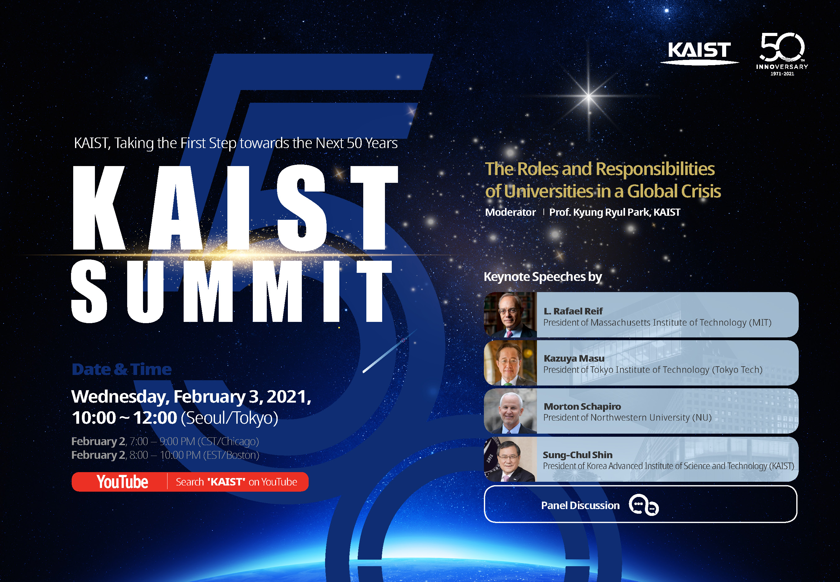 Top University Leaders Urge Innovation for the Post-COVID Era at the KAIST Summit
- Presidents of KAIST, MIT, Tokyo Tech, and Northwestern to define new roles and responsibilities of universities for the post-COVID and 4IR eras during an online summit in celebration of KAIST’s 50th anniversary. -
Universities are facing ever-mounting pressure to address impacts brought on by COVID-19 and the emerging technologies of the Fourth Industrial Revolution (4IR).
Presidents from MIT, Tokyo Tech, and Northwestern University will join the KAIST Summit to explore new directions for higher education during the post-COVID era intertwined with the 4IR. They agree that addressing these dual challenges requires pushing for innovations to rebuild the competitive edges of universities.
This summit is one of KAIST’s series of events to envision the future of KAIST and higher education in celebration of its 50th anniversary. The online summit will be live streamed on KAIST’s official YouTube channel (https://www.youtube.com/c/KAISTofficial) on February 3, 2021, from 10 a.m. to 12:00 p.m. Korean time (February 2, 7:00-9:00 p.m. CST and 8:00-10:00 p.m. EST, respectively).
The KAIST Summit titled “The Roles and Responsibilities of Universities in a Global Crisis” will discuss a range of issues affecting many aspects of universities in the coming decades.
“This summit will allow us to measure the level of risk that universities face today and will face in the future. Although there will be varying views on what a post-COVID world might look like, one thing for sure is that universities cannot go back to the way they used to exist and operate. Moreover, the 4IR continues to infiltrate and shake up our daily lives. Changes are inevitable, and universities must pursue bold and innovative responses to remain sustainable and relevant to society,” said KAIST President Sung-Chul Shin on the background of hosting the event.
The keynote speakers include KAIST President Shin, MIT President L. Rafael Reif, Tokyo Tech President Kazuya Masu, and Northwestern University President Morton Schapiro. After the keynote speech session, the speakers will take part in a panel discussion on three topics: “The Digital Divide,” “Emerging Challenges in AI,” and “Social Entrepreneurship and University-Industry Collaboration.” A Q&A session with an online audience consisting of KAIST faculty, staff, and students as well as high school students across the nation will follow shortly afterwards.
President Reif of MIT will congratulate KAIST on its successful 50-year journey from meager beginnings to achieving its current status as one of the finest global universities in science and technology. Then he will give a talk titled “Universities as Engines of Change” to present how universities have played a critical role in advancing solutions to humanity’s most urgent problems.
President Masu of Tokyo Tech will stress the importance of universities’ continuous dialogue with society as drivers of innovation. In his speech titled “Designing Our Future—Tokyo Tech DLab’s Approach,” he will introduce the activities of Tokyo Tech’s Laboratory for Design of Social Innovation in Global Networks (DLab) and explain how DLab collaborates for the future with members of society.
President Schapiro of Northwestern University will speak about how universities might incorporate the lessons they learned in dealing with COVID-19 to improve their research, teaching, and public service in the post-pandemic era. He will also look into issues arising from changing labor market needs associated with the 4IR and the aftermath of COVID-19 in his talk titled “The University in the ‘New Normal.’”
Finally, President Shin of KAIST will deliver a presentation on the “Visions & Innovations for the Next Dream of KAIST.” He will reflect on the remarkable track record from KAIST’s first 50 years and how it has contributed significantly to the rapid growth of Korea as a hi-tech powerhouse. Furthermore, he will elaborate on a new vision for the development of KAIST over the next 50 years and roll out a set of strategic innovation plans in the five areas of education, research, technology commercialization, globalization, and future strategy.
In the panel discussion, the four presidents will dive into a more intense conversation on such topics as universities’ role in bridging the increasing digital divide through their research, education, and international cooperation; the socioeconomic implications and ethical challenges of the fast deployment of AI and robotics; 4IR disruptions that will transform higher education; ways to foster social innovation and youth entrepreneurship; and how to build university-industry cooperation.
More information on KAIST’s 50th anniversary celebrations can be found on its special celebratory website at https://50.kaist.ac.kr/eng/. The official anniversary ceremony is scheduled for February 16, 2021, from 10 a.m. Korean time, and live-streaming will also be made available on KAIST’s official YouTube channel at https://www.youtube.com/c/KAISTofficial.
(END)
2021.02.01 View 15466
Top University Leaders Urge Innovation for the Post-COVID Era at the KAIST Summit
- Presidents of KAIST, MIT, Tokyo Tech, and Northwestern to define new roles and responsibilities of universities for the post-COVID and 4IR eras during an online summit in celebration of KAIST’s 50th anniversary. -
Universities are facing ever-mounting pressure to address impacts brought on by COVID-19 and the emerging technologies of the Fourth Industrial Revolution (4IR).
Presidents from MIT, Tokyo Tech, and Northwestern University will join the KAIST Summit to explore new directions for higher education during the post-COVID era intertwined with the 4IR. They agree that addressing these dual challenges requires pushing for innovations to rebuild the competitive edges of universities.
This summit is one of KAIST’s series of events to envision the future of KAIST and higher education in celebration of its 50th anniversary. The online summit will be live streamed on KAIST’s official YouTube channel (https://www.youtube.com/c/KAISTofficial) on February 3, 2021, from 10 a.m. to 12:00 p.m. Korean time (February 2, 7:00-9:00 p.m. CST and 8:00-10:00 p.m. EST, respectively).
The KAIST Summit titled “The Roles and Responsibilities of Universities in a Global Crisis” will discuss a range of issues affecting many aspects of universities in the coming decades.
“This summit will allow us to measure the level of risk that universities face today and will face in the future. Although there will be varying views on what a post-COVID world might look like, one thing for sure is that universities cannot go back to the way they used to exist and operate. Moreover, the 4IR continues to infiltrate and shake up our daily lives. Changes are inevitable, and universities must pursue bold and innovative responses to remain sustainable and relevant to society,” said KAIST President Sung-Chul Shin on the background of hosting the event.
The keynote speakers include KAIST President Shin, MIT President L. Rafael Reif, Tokyo Tech President Kazuya Masu, and Northwestern University President Morton Schapiro. After the keynote speech session, the speakers will take part in a panel discussion on three topics: “The Digital Divide,” “Emerging Challenges in AI,” and “Social Entrepreneurship and University-Industry Collaboration.” A Q&A session with an online audience consisting of KAIST faculty, staff, and students as well as high school students across the nation will follow shortly afterwards.
President Reif of MIT will congratulate KAIST on its successful 50-year journey from meager beginnings to achieving its current status as one of the finest global universities in science and technology. Then he will give a talk titled “Universities as Engines of Change” to present how universities have played a critical role in advancing solutions to humanity’s most urgent problems.
President Masu of Tokyo Tech will stress the importance of universities’ continuous dialogue with society as drivers of innovation. In his speech titled “Designing Our Future—Tokyo Tech DLab’s Approach,” he will introduce the activities of Tokyo Tech’s Laboratory for Design of Social Innovation in Global Networks (DLab) and explain how DLab collaborates for the future with members of society.
President Schapiro of Northwestern University will speak about how universities might incorporate the lessons they learned in dealing with COVID-19 to improve their research, teaching, and public service in the post-pandemic era. He will also look into issues arising from changing labor market needs associated with the 4IR and the aftermath of COVID-19 in his talk titled “The University in the ‘New Normal.’”
Finally, President Shin of KAIST will deliver a presentation on the “Visions & Innovations for the Next Dream of KAIST.” He will reflect on the remarkable track record from KAIST’s first 50 years and how it has contributed significantly to the rapid growth of Korea as a hi-tech powerhouse. Furthermore, he will elaborate on a new vision for the development of KAIST over the next 50 years and roll out a set of strategic innovation plans in the five areas of education, research, technology commercialization, globalization, and future strategy.
In the panel discussion, the four presidents will dive into a more intense conversation on such topics as universities’ role in bridging the increasing digital divide through their research, education, and international cooperation; the socioeconomic implications and ethical challenges of the fast deployment of AI and robotics; 4IR disruptions that will transform higher education; ways to foster social innovation and youth entrepreneurship; and how to build university-industry cooperation.
More information on KAIST’s 50th anniversary celebrations can be found on its special celebratory website at https://50.kaist.ac.kr/eng/. The official anniversary ceremony is scheduled for February 16, 2021, from 10 a.m. Korean time, and live-streaming will also be made available on KAIST’s official YouTube channel at https://www.youtube.com/c/KAISTofficial.
(END)
2021.02.01 View 15466 -
 Big Ideas on Emerging Materials Explored at EMS
Renowned scholars and editors from academic journals joined the Emerging Materials e-Symposium (EMS) held at KAIST and shared the latest breakthroughs and big ideas in new material development last month. This e-symposium was organized by Professor Il-Doo Kim from the KAIST Department of Materials Sciences and Engineering over five days from September 21 through 25 via Zoom and YouTube. Professor Kim also serves as an associate editor of ACS Nano.
Esteemed scholars and editors of academic journals including ACS Nano, Nano Energy, and Energy Storage Materials made Zoom presentations in three main categories: 1) nanostructures for next-generation applications, 2) chemistry and biotechnology for applications in the fields of environment and industry, and 3) material innovation for technological applications.
During Session I, speakers including Professor John A. Rogers of Northwestern University and Professor Zhenan Bao of Stanford University led the session on Emerging Soft Electronics and 3D printing.
In later sessions, other globally recognized scholars gave talks titled Advanced Nanostructuring for Emerging Materials, Frontiers in Emerging Materials Research, Advanced Energy Materials and Functional Nanomaterials, and Latest Advances in Nanomaterials Research.
These included 2010 Nobel Prize laureate and professor at Manchester University Andre Geim, editor-in-chief of ACS Nano and professor at UCLA Paul S. Weiss, Professor Paul Alivisatos of UC Berkeley, Professor William Chueh of Stanford University, and Professor Mircea Dinca of MIT.
KAIST President Sung-Chul Shin, who is also a materials physicist, said in his opening address, “Innovation in materials science will become an important driving force to change our way of life. All the breakthroughs in materials have extended a new paradigm that has transformed our lives.”
“Creative research projects alongside global collaborators like all of you will allow the breakthroughs that will deliver us from these crises,” he added.
(END)
2020.10.06 View 15469
Big Ideas on Emerging Materials Explored at EMS
Renowned scholars and editors from academic journals joined the Emerging Materials e-Symposium (EMS) held at KAIST and shared the latest breakthroughs and big ideas in new material development last month. This e-symposium was organized by Professor Il-Doo Kim from the KAIST Department of Materials Sciences and Engineering over five days from September 21 through 25 via Zoom and YouTube. Professor Kim also serves as an associate editor of ACS Nano.
Esteemed scholars and editors of academic journals including ACS Nano, Nano Energy, and Energy Storage Materials made Zoom presentations in three main categories: 1) nanostructures for next-generation applications, 2) chemistry and biotechnology for applications in the fields of environment and industry, and 3) material innovation for technological applications.
During Session I, speakers including Professor John A. Rogers of Northwestern University and Professor Zhenan Bao of Stanford University led the session on Emerging Soft Electronics and 3D printing.
In later sessions, other globally recognized scholars gave talks titled Advanced Nanostructuring for Emerging Materials, Frontiers in Emerging Materials Research, Advanced Energy Materials and Functional Nanomaterials, and Latest Advances in Nanomaterials Research.
These included 2010 Nobel Prize laureate and professor at Manchester University Andre Geim, editor-in-chief of ACS Nano and professor at UCLA Paul S. Weiss, Professor Paul Alivisatos of UC Berkeley, Professor William Chueh of Stanford University, and Professor Mircea Dinca of MIT.
KAIST President Sung-Chul Shin, who is also a materials physicist, said in his opening address, “Innovation in materials science will become an important driving force to change our way of life. All the breakthroughs in materials have extended a new paradigm that has transformed our lives.”
“Creative research projects alongside global collaborators like all of you will allow the breakthroughs that will deliver us from these crises,” he added.
(END)
2020.10.06 View 15469