Image+sensor
-
 KAIST Secures Core Technology for Ultra-High-Resolution Image Sensors
A joint research team from Korea and the United States has developed next-generation, high-resolution image sensor technology with higher power efficiency and a smaller size compared to existing sensors. Notably, they have secured foundational technology for ultra-high-resolution shortwave infrared (SWIR) image sensors, an area currently dominated by Sony, paving the way for future market entry.
KAIST (represented by President Kwang Hyung Lee) announced on the 20th of November that a research team led by Professor SangHyeon Kim from the School of Electrical Engineering, in collaboration with Inha University and Yale University in the U.S., has developed an ultra-thin broadband photodiode (PD), marking a significant breakthrough in high-performance image sensor technology.
This research drastically improves the trade-off between the absorption layer thickness and quantum efficiency found in conventional photodiode technology. Specifically, it achieved high quantum efficiency of over 70% even in an absorption layer thinner than one micrometer (μm), reducing the thickness of the absorption layer by approximately 70% compared to existing technologies.
A thinner absorption layer simplifies pixel processing, allowing for higher resolution and smoother carrier diffusion, which is advantageous for light carrier acquisition while also reducing the cost. However, a fundamental issue with thinner absorption layers is the reduced absorption of long-wavelength light.
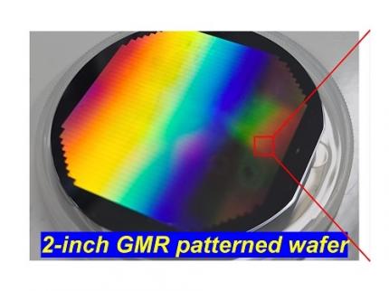
< Figure 1. Schematic diagram of the InGaAs photodiode image sensor integrated on the Guided-Mode Resonance (GMR) structure proposed in this study (left), a photograph of the fabricated wafer, and a scanning electron microscope (SEM) image of the periodic patterns (right) >
The research team introduced a guided-mode resonance (GMR) structure* that enables high-efficiency light absorption across a wide spectral range from 400 nanometers (nm) to 1,700 nanometers (nm). This wavelength range includes not only visible light but also light the SWIR region, making it valuable for various industrial applications.
*Guided-Mode Resonance (GMR) Structure: A concept used in electromagnetics, a phenomenon in which a specific (light) wave resonates (forming a strong electric/magnetic field) at a specific wavelength. Since energy is maximized under these conditions, it has been used to increase antenna or radar efficiency.
The improved performance in the SWIR region is expected to play a significant role in developing next-generation image sensors with increasingly high resolutions. The GMR structure, in particular, holds potential for further enhancing resolution and other performance metrics through hybrid integration and monolithic 3D integration with complementary metal-oxide-semiconductor (CMOS)-based readout integrated circuits (ROIC).
< Figure 2. Benchmark for state-of-the-art InGaAs-based SWIR pixels with simulated EQE lines as a function of TAL variation. Performance is maintained while reducing the absorption layer thickness from 2.1 micrometers or more to 1 micrometer or less while reducing it by 50% to 70% >
The research team has significantly enhanced international competitiveness in low-power devices and ultra-high-resolution imaging technology, opening up possibilities for applications in digital cameras, security systems, medical and industrial image sensors, as well as future ultra-high-resolution sensors for autonomous driving, aerospace, and satellite observation.
Professor Sang Hyun Kim, the lead researcher, commented, “This research demonstrates that significantly higher performance than existing technologies can be achieved even with ultra-thin absorption layers.”
< Figure 3. Top optical microscope image and cross-sectional scanning electron microscope image of the InGaAs photodiode image sensor fabricated on the GMR structure (left). Improved quantum efficiency performance of the ultra-thin image sensor (red) fabricated with the technology proposed in this study (right) >
The results of this research were published on 15th of November, in the prestigious international journal Light: Science & Applications (JCR 2.9%, IF=20.6), with Professor Dae-Myung Geum of Inha University (formerly a KAIST postdoctoral researcher) and Dr. Jinha Lim (currently a postdoctoral researcher at Yale University) as co-first authors. (Paper title: “Highly-efficient (>70%) and Wide-spectral (400 nm -1700 nm) sub-micron-thick InGaAs photodiodes for future high-resolution image sensors”)
This study was supported by the National Research Foundation of Korea.
2024.11.22 View 5540
KAIST Secures Core Technology for Ultra-High-Resolution Image Sensors
A joint research team from Korea and the United States has developed next-generation, high-resolution image sensor technology with higher power efficiency and a smaller size compared to existing sensors. Notably, they have secured foundational technology for ultra-high-resolution shortwave infrared (SWIR) image sensors, an area currently dominated by Sony, paving the way for future market entry.
KAIST (represented by President Kwang Hyung Lee) announced on the 20th of November that a research team led by Professor SangHyeon Kim from the School of Electrical Engineering, in collaboration with Inha University and Yale University in the U.S., has developed an ultra-thin broadband photodiode (PD), marking a significant breakthrough in high-performance image sensor technology.
This research drastically improves the trade-off between the absorption layer thickness and quantum efficiency found in conventional photodiode technology. Specifically, it achieved high quantum efficiency of over 70% even in an absorption layer thinner than one micrometer (μm), reducing the thickness of the absorption layer by approximately 70% compared to existing technologies.
A thinner absorption layer simplifies pixel processing, allowing for higher resolution and smoother carrier diffusion, which is advantageous for light carrier acquisition while also reducing the cost. However, a fundamental issue with thinner absorption layers is the reduced absorption of long-wavelength light.
< Figure 1. Schematic diagram of the InGaAs photodiode image sensor integrated on the Guided-Mode Resonance (GMR) structure proposed in this study (left), a photograph of the fabricated wafer, and a scanning electron microscope (SEM) image of the periodic patterns (right) >
The research team introduced a guided-mode resonance (GMR) structure* that enables high-efficiency light absorption across a wide spectral range from 400 nanometers (nm) to 1,700 nanometers (nm). This wavelength range includes not only visible light but also light the SWIR region, making it valuable for various industrial applications.
*Guided-Mode Resonance (GMR) Structure: A concept used in electromagnetics, a phenomenon in which a specific (light) wave resonates (forming a strong electric/magnetic field) at a specific wavelength. Since energy is maximized under these conditions, it has been used to increase antenna or radar efficiency.
The improved performance in the SWIR region is expected to play a significant role in developing next-generation image sensors with increasingly high resolutions. The GMR structure, in particular, holds potential for further enhancing resolution and other performance metrics through hybrid integration and monolithic 3D integration with complementary metal-oxide-semiconductor (CMOS)-based readout integrated circuits (ROIC).
< Figure 2. Benchmark for state-of-the-art InGaAs-based SWIR pixels with simulated EQE lines as a function of TAL variation. Performance is maintained while reducing the absorption layer thickness from 2.1 micrometers or more to 1 micrometer or less while reducing it by 50% to 70% >
The research team has significantly enhanced international competitiveness in low-power devices and ultra-high-resolution imaging technology, opening up possibilities for applications in digital cameras, security systems, medical and industrial image sensors, as well as future ultra-high-resolution sensors for autonomous driving, aerospace, and satellite observation.
Professor Sang Hyun Kim, the lead researcher, commented, “This research demonstrates that significantly higher performance than existing technologies can be achieved even with ultra-thin absorption layers.”
< Figure 3. Top optical microscope image and cross-sectional scanning electron microscope image of the InGaAs photodiode image sensor fabricated on the GMR structure (left). Improved quantum efficiency performance of the ultra-thin image sensor (red) fabricated with the technology proposed in this study (right) >
The results of this research were published on 15th of November, in the prestigious international journal Light: Science & Applications (JCR 2.9%, IF=20.6), with Professor Dae-Myung Geum of Inha University (formerly a KAIST postdoctoral researcher) and Dr. Jinha Lim (currently a postdoctoral researcher at Yale University) as co-first authors. (Paper title: “Highly-efficient (>70%) and Wide-spectral (400 nm -1700 nm) sub-micron-thick InGaAs photodiodes for future high-resolution image sensors”)
This study was supported by the National Research Foundation of Korea.
2024.11.22 View 5540 -
 Ultrathin but Fully Packaged High-Resolution Camera
- Biologically inspired ultrathin arrayed camera captures super-resolution images. -
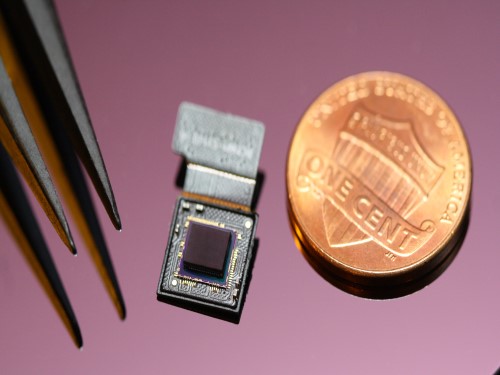
The unique structures of biological vision systems in nature inspired scientists to design ultracompact imaging systems. A research group led by Professor Ki-Hun Jeong have made an ultracompact camera that captures high-contrast and high-resolution images. Fully packaged with micro-optical elements such as inverted micro-lenses, multilayered pinhole arrays, and gap spacers on the image sensor, the camera boasts a total track length of 740 μm and a field of view of 73°.
Inspired by the eye structures of the paper wasp species Xenos peckii, the research team completely suppressed optical noise between micro-lenses while reducing camera thickness. The camera has successfully demonstrated high-contrast clear array images acquired from tiny micro lenses. To further enhance the image quality of the captured image, the team combined the arrayed images into one image through super-resolution imaging.
An insect’s compound eye has superior visual characteristics, such as a wide viewing angle, high motion sensitivity, and a large depth of field while maintaining a small volume of visual structure with a small focal length. Among them, the eyes of Xenos peckii and an endoparasite found on paper wasps have hundreds of photoreceptors in a single lens unlike conventional compound eyes. In particular, the eye structures of an adult Xenos peckii exhibit hundreds of photoreceptors on an individual eyelet and offer engineering inspiration for ultrathin cameras or imaging applications because they have higher visual acuity than other compound eyes.
For instance, Xenos peckii’s eye-inspired cameras provide a 50 times higher spatial resolution than those based on arthropod eyes. In addition, the effective image resolution of the Xenos peckii’s eye can be further improved using the image overlaps between neighboring eyelets. This unique structure offers higher visual resolution than other insect eyes.
The team achieved high-contrast and super-resolution imaging through a novel arrayed design of micro-optical elements comprising multilayered aperture arrays and inverted micro-lens arrays directly stacked over an image sensor. This optical component was integrated with a complementary metal oxide semiconductor image sensor.
This is first demonstration of super-resolution imaging which acquires a single integrated image with high contrast and high resolving power reconstructed from high-contrast array images. It is expected that this ultrathin arrayed camera can be applied for further developing mobile devices, advanced surveillance vehicles, and endoscopes.
Professor Jeong said, “This research has led to technological advances in imaging technology. We will continue to strive to make significant impacts on multidisciplinary research projects in the fields of microtechnology and nanotechnology, seeking inspiration from natural photonic structures.”
This work was featured in Light Science & Applications last month and was supported by the National Research Foundation (NRF) of and the Ministry of Health and Welfare (MOHW) of Korea.
Image credit: Professor Ki-Hun Jeong, KAIST
Image usage restrictions: News organizations may use or redistribute this image, with proper attribution, as part of news coverage of this paper only.
Publication:
Kisoo Kim, Kyung-Won Jang, Jae-Kwan Ryu, and Ki-Hun Jeong. (2020) “Biologically inspired ultrathin arrayed camera for high-contrast and high-resolution imaging”. Light Science & Applications. Volume 9. Article 28. Available online at https://doi.org/10.1038/s41377-020-0261-8
Profile:
Ki-Hun Jeong
Professor
kjeong@kaist.ac.kr
http://biophotonics.kaist.ac.kr/
Department of Bio and Brain Engineering
KAIST
Profile:
Kisoo Kim
Ph.D. Candidate
kisoo.kim1@kaist.ac.kr
http://biophotonics.kaist.ac.kr/
Department of Bio and Brain Engineering
KAIST
(END)
2020.03.23 View 20541
Ultrathin but Fully Packaged High-Resolution Camera
- Biologically inspired ultrathin arrayed camera captures super-resolution images. -
The unique structures of biological vision systems in nature inspired scientists to design ultracompact imaging systems. A research group led by Professor Ki-Hun Jeong have made an ultracompact camera that captures high-contrast and high-resolution images. Fully packaged with micro-optical elements such as inverted micro-lenses, multilayered pinhole arrays, and gap spacers on the image sensor, the camera boasts a total track length of 740 μm and a field of view of 73°.
Inspired by the eye structures of the paper wasp species Xenos peckii, the research team completely suppressed optical noise between micro-lenses while reducing camera thickness. The camera has successfully demonstrated high-contrast clear array images acquired from tiny micro lenses. To further enhance the image quality of the captured image, the team combined the arrayed images into one image through super-resolution imaging.
An insect’s compound eye has superior visual characteristics, such as a wide viewing angle, high motion sensitivity, and a large depth of field while maintaining a small volume of visual structure with a small focal length. Among them, the eyes of Xenos peckii and an endoparasite found on paper wasps have hundreds of photoreceptors in a single lens unlike conventional compound eyes. In particular, the eye structures of an adult Xenos peckii exhibit hundreds of photoreceptors on an individual eyelet and offer engineering inspiration for ultrathin cameras or imaging applications because they have higher visual acuity than other compound eyes.
For instance, Xenos peckii’s eye-inspired cameras provide a 50 times higher spatial resolution than those based on arthropod eyes. In addition, the effective image resolution of the Xenos peckii’s eye can be further improved using the image overlaps between neighboring eyelets. This unique structure offers higher visual resolution than other insect eyes.
The team achieved high-contrast and super-resolution imaging through a novel arrayed design of micro-optical elements comprising multilayered aperture arrays and inverted micro-lens arrays directly stacked over an image sensor. This optical component was integrated with a complementary metal oxide semiconductor image sensor.
This is first demonstration of super-resolution imaging which acquires a single integrated image with high contrast and high resolving power reconstructed from high-contrast array images. It is expected that this ultrathin arrayed camera can be applied for further developing mobile devices, advanced surveillance vehicles, and endoscopes.
Professor Jeong said, “This research has led to technological advances in imaging technology. We will continue to strive to make significant impacts on multidisciplinary research projects in the fields of microtechnology and nanotechnology, seeking inspiration from natural photonic structures.”
This work was featured in Light Science & Applications last month and was supported by the National Research Foundation (NRF) of and the Ministry of Health and Welfare (MOHW) of Korea.
Image credit: Professor Ki-Hun Jeong, KAIST
Image usage restrictions: News organizations may use or redistribute this image, with proper attribution, as part of news coverage of this paper only.
Publication:
Kisoo Kim, Kyung-Won Jang, Jae-Kwan Ryu, and Ki-Hun Jeong. (2020) “Biologically inspired ultrathin arrayed camera for high-contrast and high-resolution imaging”. Light Science & Applications. Volume 9. Article 28. Available online at https://doi.org/10.1038/s41377-020-0261-8
Profile:
Ki-Hun Jeong
Professor
kjeong@kaist.ac.kr
http://biophotonics.kaist.ac.kr/
Department of Bio and Brain Engineering
KAIST
Profile:
Kisoo Kim
Ph.D. Candidate
kisoo.kim1@kaist.ac.kr
http://biophotonics.kaist.ac.kr/
Department of Bio and Brain Engineering
KAIST
(END)
2020.03.23 View 20541