Engineering
-
 KAIST provides a comprehensive resource on microbial cell factories for sustainable chemical production
In silico analysis of five industrial microorganisms identifies optimal strains and metabolic engineering strategies for producing 235 valuable chemicals
Climate change and the depletion of fossil fuels have raised the global need for sustainable chemical production. In response to these environmental challenges, microbial cell factories are gaining attention as eco-friendly platforms for producing chemicals using renewable resources, while metabolic engineering technologies to enhance these cell factories are becoming crucial tools for maximizing production efficiency. However, difficulties in selecting suitable microbial strains and optimizing complex metabolic pathways continue to pose significant obstacles to practical industrial applications.
KAIST (President Kwang-Hyung Lee) announced on 27th of March that Distinguished Professor Sang Yup Lee’s research team in the Department of Chemical and Biomolecular Engineering comprehensively evaluated the production capabilities of various industrial microbial cell factories using in silico simulations and, based on these findings, identified the most suitable microbial strains for producing specific chemicals as well as optimal metabolic engineering strategies.
Previously, researchers attempted to determine the best strains and efficient metabolic engineering strategies among numerous microbial candidates through extensive biological experiments and meticulous verification processes. However, this approach required substantial time and costs. Recently, the introduction of genome-scale metabolic models (GEMs), which reconstruct the metabolic networks within an organism based on its entire genome information, has enabled systematic analysis of metabolic fluxes via computer simulations. This development offers a new way to overcome limitations of conventional experimental approaches, revolutionizing both strain selection and metabolic pathway design.
Accordingly, Professor Lee’s team at the Department of Chemical and Biomolecular Engineering, KAIST, evaluated the production capabilities of five representative industrial microorganisms—Escherichia coli, Saccharomyces cerevisiae, Bacillus subtilis, Corynebacterium glutamicum, and Pseudomonas putida—for 235 bio-based chemicals. Using GEMs, the researchers calculated both the maximum theoretical yields and the maximum achievable yields under industrial conditions for each chemical, thereby establishing criteria to identify the most suitable strains for each target compound.
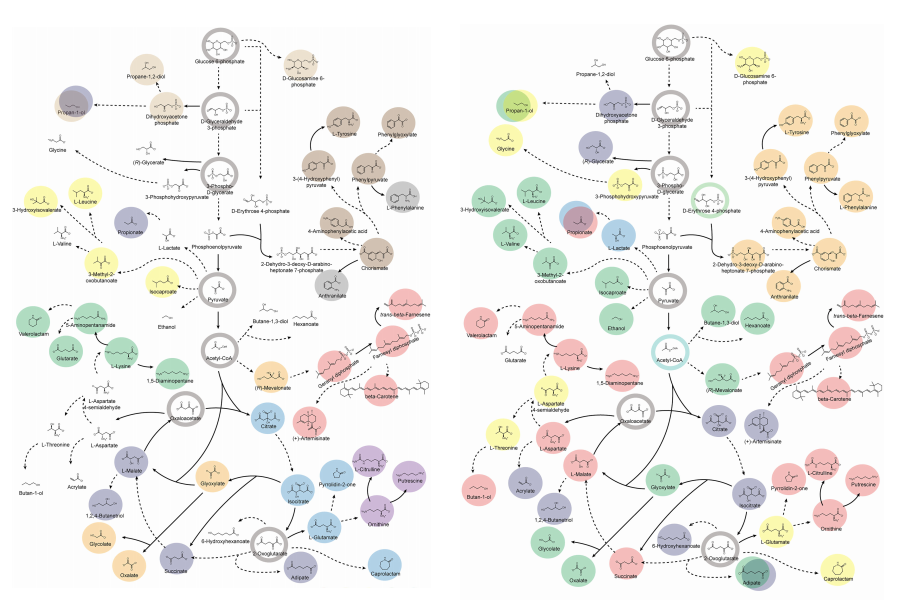
< Figure 1. Outline of the strategy for improving microbial cell factories using a genome-scale metabolic model (GEM) >
The team specifically proposed strategies such as introducing heterologous enzyme reactions derived from other organisms and exchanging cofactors used by microbes to expand metabolic pathways. These strategies were shown to increase yields beyond the innate metabolic capacities of the microorganisms, resulting in higher production of industrially important chemicals such as mevalonic acid, propanol, fatty acids, and isoprenoids.
Moreover, by applying a computational approach to analyze metabolic fluxes in silico, the researchers suggested strategies for improving microbial strains to maximize the production of various chemicals. They quantitatively identified the relationships between specific enzyme reactions and target chemical production, as well as the relationships between enzymes and metabolites, determining which enzyme reactions should be up- or down-regulated. Through this, the team presented strategies not only to achieve high theoretical yields but also to maximize actual production capacities.
< Figure 2. Comparison of production routes and maximum yields of useful chemicals using representative industrial microorganisms >
Dr. Gi Bae Kim, the first author of this paper from the KAIST BioProcess Engineering Research Center, explained, “By introducing metabolic pathways derived from other organisms and exchanging cofactors, it is possible to design new microbial cell factories that surpass existing limitations. The strategies presented in this study will play a pivotal role in making microbial-based production processes more economical and efficient.” In addition, Distinguished Professor Sang Yup Lee noted, “This research serves as a key resource in the field of systems metabolic engineering, reducing difficulties in strain selection and pathway design, and enabling more efficient development of microbial cell factories. We expect it to greatly contribute to the future development of technologies for producing various eco-friendly chemicals, such as biofuels, bioplastics, and functional food materials.”
This research was conducted with the support from the Development of platform technologies of microbial cell factories for the next-generation biorefineries project and Development of advanced synthetic biology source technologies for leading the biomanufacturing industry project (Project Leader: Distinguished Professor Sang Yup Lee, KAIST) from National Research Foundation supported by the Korean Ministry of Science and ICT.
2025.03.27 View 2069
KAIST provides a comprehensive resource on microbial cell factories for sustainable chemical production
In silico analysis of five industrial microorganisms identifies optimal strains and metabolic engineering strategies for producing 235 valuable chemicals
Climate change and the depletion of fossil fuels have raised the global need for sustainable chemical production. In response to these environmental challenges, microbial cell factories are gaining attention as eco-friendly platforms for producing chemicals using renewable resources, while metabolic engineering technologies to enhance these cell factories are becoming crucial tools for maximizing production efficiency. However, difficulties in selecting suitable microbial strains and optimizing complex metabolic pathways continue to pose significant obstacles to practical industrial applications.
KAIST (President Kwang-Hyung Lee) announced on 27th of March that Distinguished Professor Sang Yup Lee’s research team in the Department of Chemical and Biomolecular Engineering comprehensively evaluated the production capabilities of various industrial microbial cell factories using in silico simulations and, based on these findings, identified the most suitable microbial strains for producing specific chemicals as well as optimal metabolic engineering strategies.
Previously, researchers attempted to determine the best strains and efficient metabolic engineering strategies among numerous microbial candidates through extensive biological experiments and meticulous verification processes. However, this approach required substantial time and costs. Recently, the introduction of genome-scale metabolic models (GEMs), which reconstruct the metabolic networks within an organism based on its entire genome information, has enabled systematic analysis of metabolic fluxes via computer simulations. This development offers a new way to overcome limitations of conventional experimental approaches, revolutionizing both strain selection and metabolic pathway design.
Accordingly, Professor Lee’s team at the Department of Chemical and Biomolecular Engineering, KAIST, evaluated the production capabilities of five representative industrial microorganisms—Escherichia coli, Saccharomyces cerevisiae, Bacillus subtilis, Corynebacterium glutamicum, and Pseudomonas putida—for 235 bio-based chemicals. Using GEMs, the researchers calculated both the maximum theoretical yields and the maximum achievable yields under industrial conditions for each chemical, thereby establishing criteria to identify the most suitable strains for each target compound.
< Figure 1. Outline of the strategy for improving microbial cell factories using a genome-scale metabolic model (GEM) >
The team specifically proposed strategies such as introducing heterologous enzyme reactions derived from other organisms and exchanging cofactors used by microbes to expand metabolic pathways. These strategies were shown to increase yields beyond the innate metabolic capacities of the microorganisms, resulting in higher production of industrially important chemicals such as mevalonic acid, propanol, fatty acids, and isoprenoids.
Moreover, by applying a computational approach to analyze metabolic fluxes in silico, the researchers suggested strategies for improving microbial strains to maximize the production of various chemicals. They quantitatively identified the relationships between specific enzyme reactions and target chemical production, as well as the relationships between enzymes and metabolites, determining which enzyme reactions should be up- or down-regulated. Through this, the team presented strategies not only to achieve high theoretical yields but also to maximize actual production capacities.
< Figure 2. Comparison of production routes and maximum yields of useful chemicals using representative industrial microorganisms >
Dr. Gi Bae Kim, the first author of this paper from the KAIST BioProcess Engineering Research Center, explained, “By introducing metabolic pathways derived from other organisms and exchanging cofactors, it is possible to design new microbial cell factories that surpass existing limitations. The strategies presented in this study will play a pivotal role in making microbial-based production processes more economical and efficient.” In addition, Distinguished Professor Sang Yup Lee noted, “This research serves as a key resource in the field of systems metabolic engineering, reducing difficulties in strain selection and pathway design, and enabling more efficient development of microbial cell factories. We expect it to greatly contribute to the future development of technologies for producing various eco-friendly chemicals, such as biofuels, bioplastics, and functional food materials.”
This research was conducted with the support from the Development of platform technologies of microbial cell factories for the next-generation biorefineries project and Development of advanced synthetic biology source technologies for leading the biomanufacturing industry project (Project Leader: Distinguished Professor Sang Yup Lee, KAIST) from National Research Foundation supported by the Korean Ministry of Science and ICT.
2025.03.27 View 2069 -
 KAIST Develops Eco-Friendly, Nylon-Like Plastic Using Microorganisms
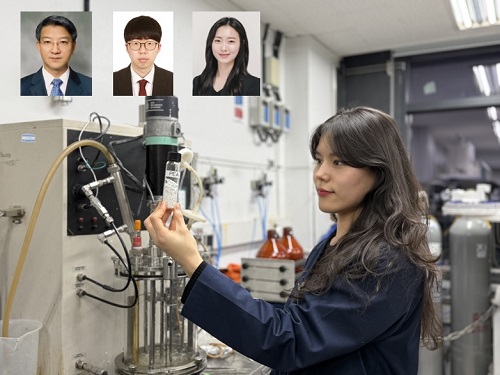
Poly(ester amide) amide is a next-generation material that combines the advantages of PET (polyester) and nylon (polyamide), two widely used plastics. However, it could only be produced from fossil fuels, which posed environmental concerns. Using microorganisms, KAIST researchers have successfully developed a new bio-based plastic to replace conventional plastic.
KAIST (represented by President Kwang Hyung Lee) announced on the 20th of March that a research team led by Distinguished Professor Sang Yup Lee from the Department of Chemical and Biomolecular Engineering has developed microbial strains through systems metabolic engineering to produce various eco-friendly, bio-based poly(ester amide)s. The team collaborated with researchers from the Korea Research Institute of Chemical Technology (KRICT, President Young-Kook Lee) to analyze and confirm the properties of the resulting plastic.
Professor Sang Yup Lee’s research team designed new metabolic pathways that do not naturally exist in microorganisms, and developed a platform microbial strain capable of producing nine different types of poly(ester amide)s, including poly(3-hydroxybutyrate-ran-3-aminopropionate) and poly(3-hydroxybutyrate-ran-4-aminobutyrate).
Using glucose derived from abundant biomass sources such as waste wood and weeds, the team successfully produced poly(ester amide)s in an eco-friendly manner. The researchers also confirmed the potential for industrial-scale production by demonstrating high production efficiency (54.57 g/L) using fed-batch fermentation of the engineered strain.
In collaboration with researchers Haemin Jeong and Jihoon Shin from KRICT, the KAIST team analyzed the properties of the bio-based plastic and found that it exhibited characteristics similar to high-density polyethylene (HDPE). This means the new plastic is not only eco-friendly but also strong and durable enough to replace conventional plastics.
The engineered strains and strategies developed in this study are expected to be useful not only for producing various poly(ester amide)s but also for constructing metabolic pathways for the biosynthesis of other types of polymers.
Professor Sang Yup Lee stated, “This study is the first to demonstrate the possibility of producing poly(ester amide)s (plastics) through a renewable bio-based chemical process rather than relying on the petroleum-based chemical industry. We plan to further enhance the production yield and efficiency through continued research.”
The study was published online on March 17 in the international journal Nature Chemical Biology.
·Title: Biosynthesis of poly(ester amide)s in engineered Escherichia coli
·DOI: 10.1038/s41589-025-01842-2
·Authors: A total of seven authors including Tong Un Chae (KAIST, first author), So Young Choi (KAIST, second author), Da-Hee Ahn (KAIST, third author), Woo Dae Jang (KAIST, fourth author), Haemin Jeong (KRICT, fifth author), Jihoon Shin (KRICT, sixth author), and Sang Yup Lee (KAIST, corresponding author).
This research was supported by the Ministry of Science and ICT (MSIT) under the Eco-Friendly Chemical Technology Development Project as part of the "Next-Generation Biorefinery Technology Development to Lead the Bio-Chemical Industry" initiative (project led by Distinguished Professor Sang Yup Lee at KAIST).
2025.03.24 View 3090
KAIST Develops Eco-Friendly, Nylon-Like Plastic Using Microorganisms
Poly(ester amide) amide is a next-generation material that combines the advantages of PET (polyester) and nylon (polyamide), two widely used plastics. However, it could only be produced from fossil fuels, which posed environmental concerns. Using microorganisms, KAIST researchers have successfully developed a new bio-based plastic to replace conventional plastic.
KAIST (represented by President Kwang Hyung Lee) announced on the 20th of March that a research team led by Distinguished Professor Sang Yup Lee from the Department of Chemical and Biomolecular Engineering has developed microbial strains through systems metabolic engineering to produce various eco-friendly, bio-based poly(ester amide)s. The team collaborated with researchers from the Korea Research Institute of Chemical Technology (KRICT, President Young-Kook Lee) to analyze and confirm the properties of the resulting plastic.
Professor Sang Yup Lee’s research team designed new metabolic pathways that do not naturally exist in microorganisms, and developed a platform microbial strain capable of producing nine different types of poly(ester amide)s, including poly(3-hydroxybutyrate-ran-3-aminopropionate) and poly(3-hydroxybutyrate-ran-4-aminobutyrate).
Using glucose derived from abundant biomass sources such as waste wood and weeds, the team successfully produced poly(ester amide)s in an eco-friendly manner. The researchers also confirmed the potential for industrial-scale production by demonstrating high production efficiency (54.57 g/L) using fed-batch fermentation of the engineered strain.
In collaboration with researchers Haemin Jeong and Jihoon Shin from KRICT, the KAIST team analyzed the properties of the bio-based plastic and found that it exhibited characteristics similar to high-density polyethylene (HDPE). This means the new plastic is not only eco-friendly but also strong and durable enough to replace conventional plastics.
The engineered strains and strategies developed in this study are expected to be useful not only for producing various poly(ester amide)s but also for constructing metabolic pathways for the biosynthesis of other types of polymers.
Professor Sang Yup Lee stated, “This study is the first to demonstrate the possibility of producing poly(ester amide)s (plastics) through a renewable bio-based chemical process rather than relying on the petroleum-based chemical industry. We plan to further enhance the production yield and efficiency through continued research.”
The study was published online on March 17 in the international journal Nature Chemical Biology.
·Title: Biosynthesis of poly(ester amide)s in engineered Escherichia coli
·DOI: 10.1038/s41589-025-01842-2
·Authors: A total of seven authors including Tong Un Chae (KAIST, first author), So Young Choi (KAIST, second author), Da-Hee Ahn (KAIST, third author), Woo Dae Jang (KAIST, fourth author), Haemin Jeong (KRICT, fifth author), Jihoon Shin (KRICT, sixth author), and Sang Yup Lee (KAIST, corresponding author).
This research was supported by the Ministry of Science and ICT (MSIT) under the Eco-Friendly Chemical Technology Development Project as part of the "Next-Generation Biorefinery Technology Development to Lead the Bio-Chemical Industry" initiative (project led by Distinguished Professor Sang Yup Lee at KAIST).
2025.03.24 View 3090 -
 Ultralight advanced material developed by KAIST and U of Toronto
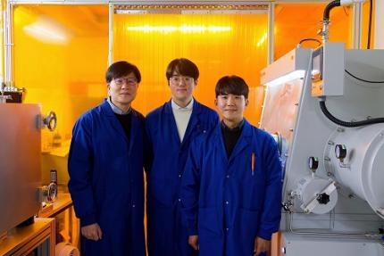
< (From left) Professor Seunghwa Ryu of KAIST Department of Mechanical Engineering, Professor Tobin Filleter of the University of Toronto, Dr. Jinwook Yeo of KAIST, and Dr. Peter Serles of the University of Toronto >
Recently, in advanced industries such as automobiles, aerospace, and mobility, there has been increasing demand for materials that achieve weight reduction while maintaining excellent mechanical properties. An international joint research team has developed an ultralight, high-strength material utilizing nanostructures, presenting the potential for various industrial applications through customized design in the future.
KAIST (represented by President Kwang Hyung Lee) announced on the 18th of February that a research team led by Professor Seunghwa Ryu from the Department of Mechanical Engineering, in collaboration with Professor Tobin Filleter from the University of Toronto, has developed a nano-lattice structure that maximizes lightweight properties while maintaining high stiffness and strength.
In this study, the research team optimized the beam shape of the lattice structure to maintain its lightweight characteristics while maximizing stiffness and strength.
Particularly, using a multi-objective Bayesian optimization algorithm*, the team conducted an optimal design process that simultaneously considers tensile and shear stiffness improvement and weight reduction. They demonstrated that the optimal lattice structure could be predicted and designed with significantly less data (about 400 data points) compared to conventional methods.
*Multi-objective Bayesian optimization algorithm: A method that finds the optimal solution while considering multiple objectives simultaneously. It efficiently collects data and predicts results even under conditions of uncertainty.
< Figure 1. Multi-objective Bayesian optimization for generative design of carbon nanolattices with high compressive stiffness and strength at low density. The upper is the illustration of process workflow. The lower part shows top four MBO CFCC geometries with their 2D Bézier curves. (The optimized structure is predicted and designed with much less data (approximately 400) than the conventional method >
Furthermore, to maximize the effect where mechanical properties improve as size decreases at the nanoscale, the research team utilized pyrolytic carbon* material to implement an ultralight, high-strength, high-stiffness nano-lattice structure.
*Pyrolytic carbon: A carbon material obtained by decomposing organic substances at high temperatures. It has excellent heat resistance and strength, making it widely used in industries such as semiconductor equipment coatings and artificial joint coatings, where it must withstand high temperatures without deformation.
For this, the team applied two-photon polymerization (2PP) technology* to precisely fabricate complex nano-lattice structures, and mechanical performance evaluations confirmed that the developed structure simultaneously possesses strength comparable to steel and the lightness of Styrofoam.
*Two-photon polymerization (2PP) technology: An advanced optical manufacturing technique based on the principle that polymerization occurs only when two photons of a specific wavelength are absorbed simultaneously.
Additionally, the research team demonstrated that multi-focus two-photon polymerization (multi-focus 2PP) technology enables the fabrication of millimeter-scale structures while maintaining nanoscale precision.
Professor Seunghwa Ryu explained, "This technology innovatively solves the stress concentration issue, which has been a limitation of conventional design methods, through three-dimensional nano-lattice structures, achieving both ultralight weight and high strength in material development."
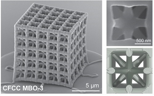
< Figure 2. FESEM image of the fabricated nano-lattice structure and (bottom right) the macroscopic nanolattice resting on a bubble >
He further emphasized, "By integrating data-driven optimal design with precision 3D printing technology, this development not only meets the demand for lightweight materials in the aerospace and automotive industries but also opens possibilities for various industrial applications through customized design."
This study was led by Dr. Peter Serles of the Department of Mechanical & Industrial Engineering at University of Toronto and Dr. Jinwook Yeo from KAIST as co-first authors, with Professor Seunghwa Ryu and Professor Tobin Filleter as corresponding authors.
The research was published on January 23, 2025 in the international journal Advanced Materials (Paper title: “Ultrahigh Specific Strength by Bayesian Optimization of Lightweight Carbon Nanolattices”).
DOI: https://doi.org/10.1002/adma.202410651
This research was supported by the Multiphase Materials Innovation Manufacturing Research Center (an ERC program) funded by the Ministry of Science and ICT, the M3DT (Medical Device Digital Development Tool) project funded by the Ministry of Food and Drug Safety, and the KAIST International Collaboration Program.
2025.02.18 View 3074
Ultralight advanced material developed by KAIST and U of Toronto
< (From left) Professor Seunghwa Ryu of KAIST Department of Mechanical Engineering, Professor Tobin Filleter of the University of Toronto, Dr. Jinwook Yeo of KAIST, and Dr. Peter Serles of the University of Toronto >
Recently, in advanced industries such as automobiles, aerospace, and mobility, there has been increasing demand for materials that achieve weight reduction while maintaining excellent mechanical properties. An international joint research team has developed an ultralight, high-strength material utilizing nanostructures, presenting the potential for various industrial applications through customized design in the future.
KAIST (represented by President Kwang Hyung Lee) announced on the 18th of February that a research team led by Professor Seunghwa Ryu from the Department of Mechanical Engineering, in collaboration with Professor Tobin Filleter from the University of Toronto, has developed a nano-lattice structure that maximizes lightweight properties while maintaining high stiffness and strength.
In this study, the research team optimized the beam shape of the lattice structure to maintain its lightweight characteristics while maximizing stiffness and strength.
Particularly, using a multi-objective Bayesian optimization algorithm*, the team conducted an optimal design process that simultaneously considers tensile and shear stiffness improvement and weight reduction. They demonstrated that the optimal lattice structure could be predicted and designed with significantly less data (about 400 data points) compared to conventional methods.
*Multi-objective Bayesian optimization algorithm: A method that finds the optimal solution while considering multiple objectives simultaneously. It efficiently collects data and predicts results even under conditions of uncertainty.
< Figure 1. Multi-objective Bayesian optimization for generative design of carbon nanolattices with high compressive stiffness and strength at low density. The upper is the illustration of process workflow. The lower part shows top four MBO CFCC geometries with their 2D Bézier curves. (The optimized structure is predicted and designed with much less data (approximately 400) than the conventional method >
Furthermore, to maximize the effect where mechanical properties improve as size decreases at the nanoscale, the research team utilized pyrolytic carbon* material to implement an ultralight, high-strength, high-stiffness nano-lattice structure.
*Pyrolytic carbon: A carbon material obtained by decomposing organic substances at high temperatures. It has excellent heat resistance and strength, making it widely used in industries such as semiconductor equipment coatings and artificial joint coatings, where it must withstand high temperatures without deformation.
For this, the team applied two-photon polymerization (2PP) technology* to precisely fabricate complex nano-lattice structures, and mechanical performance evaluations confirmed that the developed structure simultaneously possesses strength comparable to steel and the lightness of Styrofoam.
*Two-photon polymerization (2PP) technology: An advanced optical manufacturing technique based on the principle that polymerization occurs only when two photons of a specific wavelength are absorbed simultaneously.
Additionally, the research team demonstrated that multi-focus two-photon polymerization (multi-focus 2PP) technology enables the fabrication of millimeter-scale structures while maintaining nanoscale precision.
Professor Seunghwa Ryu explained, "This technology innovatively solves the stress concentration issue, which has been a limitation of conventional design methods, through three-dimensional nano-lattice structures, achieving both ultralight weight and high strength in material development."
< Figure 2. FESEM image of the fabricated nano-lattice structure and (bottom right) the macroscopic nanolattice resting on a bubble >
He further emphasized, "By integrating data-driven optimal design with precision 3D printing technology, this development not only meets the demand for lightweight materials in the aerospace and automotive industries but also opens possibilities for various industrial applications through customized design."
This study was led by Dr. Peter Serles of the Department of Mechanical & Industrial Engineering at University of Toronto and Dr. Jinwook Yeo from KAIST as co-first authors, with Professor Seunghwa Ryu and Professor Tobin Filleter as corresponding authors.
The research was published on January 23, 2025 in the international journal Advanced Materials (Paper title: “Ultrahigh Specific Strength by Bayesian Optimization of Lightweight Carbon Nanolattices”).
DOI: https://doi.org/10.1002/adma.202410651
This research was supported by the Multiphase Materials Innovation Manufacturing Research Center (an ERC program) funded by the Ministry of Science and ICT, the M3DT (Medical Device Digital Development Tool) project funded by the Ministry of Food and Drug Safety, and the KAIST International Collaboration Program.
2025.02.18 View 3074 -
 KAIST Develops Wearable Carbon Dioxide Sensor to Enable Real-time Apnea Diagnosis
- Professor Seunghyup Yoo’s research team of the School of Electrical Engineering developed an ultralow-power carbon dioxide (CO2) sensor using a flexible and thin organic photodiode, and succeeded in real-time breathing monitoring by attaching it to a commercial mask
- Wearable devices with features such as low power, high stability, and flexibility can be utilized for early diagnosis of various diseases such as chronic obstructive pulmonary disease and sleep apnea
< Photo 1. From the left, School of Electrical Engineering, Ph.D. candidate DongHo Choi, Professor Seunghyup Yoo, and Department of Materials Science and Engineering, Bachelor’s candidate MinJae Kim >
Carbon dioxide (CO2) is a major respiratory metabolite, and continuous monitoring of CO2 concentration in exhaled breath is not only an important indicator for early detection and diagnosis of respiratory and circulatory system diseases, but can also be widely used for monitoring personal exercise status. KAIST researchers succeeded in accurately measuring CO2 concentration by attaching it to the inside of a mask.
KAIST (President Kwang-Hyung Lee) announced on February 10th that Professor Seunghyup Yoo's research team in the Department of Electrical and Electronic Engineering developed a low-power, high-speed wearable CO2 sensor capable of stable breathing monitoring in real time.
Existing non-invasive CO2 sensors had limitations in that they were large in size and consumed high power. In particular, optochemical CO2 sensors using fluorescent molecules have the advantage of being miniaturized and lightweight, but due to the photodegradation phenomenon of dye molecules, they are difficult to use stably for a long time, which limits their use as wearable healthcare sensors.
Optochemical CO2 sensors utilize the fact that the intensity of fluorescence emitted from fluorescent molecules decreases depending on the concentration of CO2, and it is important to effectively detect changes in fluorescence light.
To this end, the research team developed a low-power CO2 sensor consisting of an LED and an organic photodiode surrounding it. Based on high light collection efficiency, the sensor, which minimizes the amount of excitation light irradiated on fluorescent molecules, achieved a device power consumption of 171 μW, which is tens of times lower than existing sensors that consume several mW.
< Figure 1. Structure and operating principle of the developed optochemical carbon dioxide (CO2) sensor. Light emitted from the LED is converted into fluorescence through the fluorescent film, reflected from the light scattering layer, and incident on the organic photodiode. CO2 reacts with a small amount of water inside the fluorescent film to form carbonic acid (H2CO3), which increases the concentration of hydrogen ions (H+), and the fluorescence intensity due to 470 nm excitation light decreases. The circular organic photodiode with high light collection efficiency effectively detects changes in fluorescence intensity, lowers the power required light up the LED, and reduces light-induced deterioration. >
The research team also elucidated the photodegradation path of fluorescent molecules used in CO2 sensors, revealed the cause of the increase in error over time in photochemical sensors, and suggested an optical design method to suppress the occurrence of errors.
Based on this, the research team developed a sensor that effectively reduces errors caused by photodegradation, which was a chronic problem of existing photochemical sensors, and can be used continuously for up to 9 hours while existing technologies based on the same material can be used for less than 20 minutes, and can be used multiple times when replacing the CO2 detection fluorescent film.
< Figure 2. Wearable smart mask and real-time breathing monitoring. The fabricated sensor module consists of four elements (①: gas-permeable light-scattering layer, ②: color filter and organic photodiode, ③: light-emitting diode, ④: CO2-detecting fluorescent film). The thin and light sensor (D1: 400 nm, D2: 470 nm) is attached to the inside of the mask to monitor the wearer's breathing in real time. >
The developed sensor accurately measured CO2 concentration by being attached to the inside of a mask based on the advantages of being light (0.12 g), thin (0.7 mm), and flexible. In addition, it showed fast speed and high resolution that can monitor respiratory rate by distinguishing between inhalation and exhalation in real time.
< Photo 2. The developed sensor attached to the inside of the mask >
Professor Seunghyup Yoo said, "The developed sensor has excellent characteristics such as low power, high stability, and flexibility, so it can be widely applied to wearable devices, and can be used for the early diagnosis of various diseases such as hypercapnia, chronic obstructive pulmonary disease, and sleep apnea." He added, "In particular, it is expected to be used to improve side effects caused by rebreathing in environments where dust is generated or where masks are worn for long periods of time, such as during seasonal changes."
This study, in which KAIST's Department of Materials Science and Engineering's undergraduate student Minjae Kim and School of Electrical Engineering's doctoral student Dongho Choi participated as joint first authors, was published in the online version of Cell's sister journal, Device, on the 22nd of last month. (Paper title: Ultralow-power carbon dioxide sensor for real-time breath monitoring) DOI: https://doi.org/10.1016/j.device.2024.100681
< Photo 3. From the left, Professor Seunghyup Yoo of the School of Electrical Engineering, MinJae Kim, an undergraduate student in the Department of Materials Science and Engineering, and Dongho Choi, a doctoral student in the School of Electrical Engineering >
This study was supported by the Ministry of Trade, Industry and Energy's Materials and Components Technology Development Project, the National Research Foundation of Korea's Original Technology Development Project, and the KAIST Undergraduate Research Participation Project. This work was supported by the (URP) program.
2025.02.13 View 4224
KAIST Develops Wearable Carbon Dioxide Sensor to Enable Real-time Apnea Diagnosis
- Professor Seunghyup Yoo’s research team of the School of Electrical Engineering developed an ultralow-power carbon dioxide (CO2) sensor using a flexible and thin organic photodiode, and succeeded in real-time breathing monitoring by attaching it to a commercial mask
- Wearable devices with features such as low power, high stability, and flexibility can be utilized for early diagnosis of various diseases such as chronic obstructive pulmonary disease and sleep apnea
< Photo 1. From the left, School of Electrical Engineering, Ph.D. candidate DongHo Choi, Professor Seunghyup Yoo, and Department of Materials Science and Engineering, Bachelor’s candidate MinJae Kim >
Carbon dioxide (CO2) is a major respiratory metabolite, and continuous monitoring of CO2 concentration in exhaled breath is not only an important indicator for early detection and diagnosis of respiratory and circulatory system diseases, but can also be widely used for monitoring personal exercise status. KAIST researchers succeeded in accurately measuring CO2 concentration by attaching it to the inside of a mask.
KAIST (President Kwang-Hyung Lee) announced on February 10th that Professor Seunghyup Yoo's research team in the Department of Electrical and Electronic Engineering developed a low-power, high-speed wearable CO2 sensor capable of stable breathing monitoring in real time.
Existing non-invasive CO2 sensors had limitations in that they were large in size and consumed high power. In particular, optochemical CO2 sensors using fluorescent molecules have the advantage of being miniaturized and lightweight, but due to the photodegradation phenomenon of dye molecules, they are difficult to use stably for a long time, which limits their use as wearable healthcare sensors.
Optochemical CO2 sensors utilize the fact that the intensity of fluorescence emitted from fluorescent molecules decreases depending on the concentration of CO2, and it is important to effectively detect changes in fluorescence light.
To this end, the research team developed a low-power CO2 sensor consisting of an LED and an organic photodiode surrounding it. Based on high light collection efficiency, the sensor, which minimizes the amount of excitation light irradiated on fluorescent molecules, achieved a device power consumption of 171 μW, which is tens of times lower than existing sensors that consume several mW.
< Figure 1. Structure and operating principle of the developed optochemical carbon dioxide (CO2) sensor. Light emitted from the LED is converted into fluorescence through the fluorescent film, reflected from the light scattering layer, and incident on the organic photodiode. CO2 reacts with a small amount of water inside the fluorescent film to form carbonic acid (H2CO3), which increases the concentration of hydrogen ions (H+), and the fluorescence intensity due to 470 nm excitation light decreases. The circular organic photodiode with high light collection efficiency effectively detects changes in fluorescence intensity, lowers the power required light up the LED, and reduces light-induced deterioration. >
The research team also elucidated the photodegradation path of fluorescent molecules used in CO2 sensors, revealed the cause of the increase in error over time in photochemical sensors, and suggested an optical design method to suppress the occurrence of errors.
Based on this, the research team developed a sensor that effectively reduces errors caused by photodegradation, which was a chronic problem of existing photochemical sensors, and can be used continuously for up to 9 hours while existing technologies based on the same material can be used for less than 20 minutes, and can be used multiple times when replacing the CO2 detection fluorescent film.
< Figure 2. Wearable smart mask and real-time breathing monitoring. The fabricated sensor module consists of four elements (①: gas-permeable light-scattering layer, ②: color filter and organic photodiode, ③: light-emitting diode, ④: CO2-detecting fluorescent film). The thin and light sensor (D1: 400 nm, D2: 470 nm) is attached to the inside of the mask to monitor the wearer's breathing in real time. >
The developed sensor accurately measured CO2 concentration by being attached to the inside of a mask based on the advantages of being light (0.12 g), thin (0.7 mm), and flexible. In addition, it showed fast speed and high resolution that can monitor respiratory rate by distinguishing between inhalation and exhalation in real time.
< Photo 2. The developed sensor attached to the inside of the mask >
Professor Seunghyup Yoo said, "The developed sensor has excellent characteristics such as low power, high stability, and flexibility, so it can be widely applied to wearable devices, and can be used for the early diagnosis of various diseases such as hypercapnia, chronic obstructive pulmonary disease, and sleep apnea." He added, "In particular, it is expected to be used to improve side effects caused by rebreathing in environments where dust is generated or where masks are worn for long periods of time, such as during seasonal changes."
This study, in which KAIST's Department of Materials Science and Engineering's undergraduate student Minjae Kim and School of Electrical Engineering's doctoral student Dongho Choi participated as joint first authors, was published in the online version of Cell's sister journal, Device, on the 22nd of last month. (Paper title: Ultralow-power carbon dioxide sensor for real-time breath monitoring) DOI: https://doi.org/10.1016/j.device.2024.100681
< Photo 3. From the left, Professor Seunghyup Yoo of the School of Electrical Engineering, MinJae Kim, an undergraduate student in the Department of Materials Science and Engineering, and Dongho Choi, a doctoral student in the School of Electrical Engineering >
This study was supported by the Ministry of Trade, Industry and Energy's Materials and Components Technology Development Project, the National Research Foundation of Korea's Original Technology Development Project, and the KAIST Undergraduate Research Participation Project. This work was supported by the (URP) program.
2025.02.13 View 4224 -
 KAIST Develops AI-Driven Performance Prediction Model to Advance Space Electric Propulsion Technology
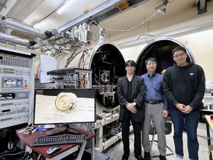
< (From left) PhD candidate Youngho Kim, Professor Wonho Choe, and PhD candidate Jaehong Park from the Department of Nuclear and Quantum Engineering >
Hall thrusters, a key space technology for missions like SpaceX's Starlink constellation and NASA's Psyche asteroid mission, are high-efficiency electric propulsion devices using plasma technology*. The KAIST research team announced that the AI-designed Hall thruster developed for CubeSats will be installed on the KAIST-Hall Effect Rocket Orbiter (K-HERO) CubeSat to demonstrate its in-orbit performance during the fourth launch of the Korean Launch Vehicle called Nuri rocket (KSLV-2) scheduled for November this year.
*Plasma is one of the four states of matter, where gases are heated to high energies, causing them to separate into charged ions and electrons. Plasma is used not only in space electric propulsion but also in semiconductor manufacturing, display processes, and sterilization devices.
On February 3rd, the research team from the KAIST Department of Nuclear and Quantum Engineering’s Electric Propulsion Laboratory, led by Professor Wonho Choe, announced the development of an AI-based technique to accurately predict the performance of Hall thrusters, the engines of satellites and space probes.
Hall thrusters provide high fuel efficiency, requiring minimal propellant to achieve significant acceleration of spacecrafts or satellites while producing substantial thrust relative to power consumption. Due to these advantages, Hall thrusters are widely used in various space missions, including the formation flight of satellite constellations, deorbiting maneuvers for space debris mitigation, and deep space missions such as asteroid exploration.
As the space industry continues to grow during the NewSpace era, the demand for Hall thrusters suited to diverse missions is increasing. To rapidly develop highly efficient, mission-optimized Hall thrusters, it is essential to predict thruster performance accurately from the design phase.
However, conventional methods have limitations, as they struggle to handle the complex plasma phenomena within Hall thrusters or are only applicable under specific conditions, leading to lower prediction accuracy.
The research team developed an AI-based performance prediction technique with high accuracy, significantly reducing the time and cost associated with the iterative design, fabrication, and testing of thrusters. Since 2003, Professor Wonho Choe’s team has been leading research on electric propulsion development in Korea. The team applied a neural network ensemble model to predict thruster performance using 18,000 Hall thruster training data points generated from their in-house numerical simulation tool.
The in-house numerical simulation tool, developed to model plasma physics and thrust performance, played a crucial role in providing high-quality training data. The simulation’s accuracy was validated through comparisons with experimental data from ten KAIST in-house Hall thrusters, with an average prediction error of less than 10%.
< Figure 1. This research has been selected as the cover article for the March 2025 issue (Volume 7, Issue 3) of the AI interdisciplinary journal, Advanced Intelligent Systems. >
The trained neural network ensemble model acts as a digital twin, accurately predicting the Hall thruster performance within seconds based on thruster design variables.
Notably, it offers detailed analyses of performance parameters such as thrust and discharge current, accounting for Hall thruster design variables like propellant flow rate and magnetic field—factors that are challenging to evaluate using traditional scaling laws.
This AI model demonstrated an average prediction error of less than 5% for the in-house 700 W and 1 kW KAIST Hall thrusters and less than 9% for a 5 kW high-power Hall thruster developed by the University of Michigan and the U.S. Air Force Research Laboratory. This confirms the broad applicability of the AI prediction method across different power levels of Hall thrusters.
Professor Wonho Choe stated, “The AI-based prediction technique developed by our team is highly accurate and is already being utilized in the analysis of thrust performance and the development of highly efficient, low-power Hall thrusters for satellites and spacecraft. This AI approach can also be applied beyond Hall thrusters to various industries, including semiconductor manufacturing, surface processing, and coating, through ion beam sources.”
< Figure 2. The AI-based prediction technique developed by the research team accurately predicts thrust performance based on design variables, making it highly valuable for the development of high-efficiency Hall thrusters. The neural network ensemble processes design variables, such as channel geometry and magnetic field information, and outputs key performance metrics like thrust and prediction accuracy, enabling efficient thruster design and performance analysis. >
Additionally, Professor Choe mentioned, “The CubeSat Hall thruster, developed using the AI technique in collaboration with our lab startup—Cosmo Bee, an electric propulsion company—will be tested in orbit this November aboard the K-HERO 3U (30 x 10 x 10 cm) CubeSat, scheduled for launch on the fourth flight of the KSLV-2 Nuri rocket.”
This research was published online in Advanced Intelligent Systems on December 25, 2024 with PhD candidate Jaehong Park as the first author and was selected as the journal’s cover article, highlighting its innovation.
< Figure 3. Image of the 150 W low-power Hall thruster for small and micro satellites, developed in collaboration with Cosmo Bee and the KAIST team. The thruster will be tested in orbit on the K-HERO CubeSat during the KSLV-2 Nuri rocket’s fourth launch in Q4 2025. >
This research was supported by the National Research Foundation of Korea’s Space Pioneer Program (200mN High Thrust Electric Propulsion System Development).
(Paper Title: Predicting Performance of Hall Effect Ion Source Using Machine Learning, DOI: https://doi.org/10.1002/aisy.202400555 )
< Figure 4. Graphs of the predicted thrust and discharge current of KAIST’s 700 W Hall thruster using the AI model (HallNN). The left image shows the Hall thruster operating in KAIST Electric Propulsion Laboratory’s vacuum chamber, while the center and right graphs present the prediction results for thrust and discharge current based on anode mass flow rate. The red lines represent AI predictions, and the blue dots represent experimental results, with a prediction error of less than 5%. >
2025.02.03 View 4114
KAIST Develops AI-Driven Performance Prediction Model to Advance Space Electric Propulsion Technology
< (From left) PhD candidate Youngho Kim, Professor Wonho Choe, and PhD candidate Jaehong Park from the Department of Nuclear and Quantum Engineering >
Hall thrusters, a key space technology for missions like SpaceX's Starlink constellation and NASA's Psyche asteroid mission, are high-efficiency electric propulsion devices using plasma technology*. The KAIST research team announced that the AI-designed Hall thruster developed for CubeSats will be installed on the KAIST-Hall Effect Rocket Orbiter (K-HERO) CubeSat to demonstrate its in-orbit performance during the fourth launch of the Korean Launch Vehicle called Nuri rocket (KSLV-2) scheduled for November this year.
*Plasma is one of the four states of matter, where gases are heated to high energies, causing them to separate into charged ions and electrons. Plasma is used not only in space electric propulsion but also in semiconductor manufacturing, display processes, and sterilization devices.
On February 3rd, the research team from the KAIST Department of Nuclear and Quantum Engineering’s Electric Propulsion Laboratory, led by Professor Wonho Choe, announced the development of an AI-based technique to accurately predict the performance of Hall thrusters, the engines of satellites and space probes.
Hall thrusters provide high fuel efficiency, requiring minimal propellant to achieve significant acceleration of spacecrafts or satellites while producing substantial thrust relative to power consumption. Due to these advantages, Hall thrusters are widely used in various space missions, including the formation flight of satellite constellations, deorbiting maneuvers for space debris mitigation, and deep space missions such as asteroid exploration.
As the space industry continues to grow during the NewSpace era, the demand for Hall thrusters suited to diverse missions is increasing. To rapidly develop highly efficient, mission-optimized Hall thrusters, it is essential to predict thruster performance accurately from the design phase.
However, conventional methods have limitations, as they struggle to handle the complex plasma phenomena within Hall thrusters or are only applicable under specific conditions, leading to lower prediction accuracy.
The research team developed an AI-based performance prediction technique with high accuracy, significantly reducing the time and cost associated with the iterative design, fabrication, and testing of thrusters. Since 2003, Professor Wonho Choe’s team has been leading research on electric propulsion development in Korea. The team applied a neural network ensemble model to predict thruster performance using 18,000 Hall thruster training data points generated from their in-house numerical simulation tool.
The in-house numerical simulation tool, developed to model plasma physics and thrust performance, played a crucial role in providing high-quality training data. The simulation’s accuracy was validated through comparisons with experimental data from ten KAIST in-house Hall thrusters, with an average prediction error of less than 10%.
< Figure 1. This research has been selected as the cover article for the March 2025 issue (Volume 7, Issue 3) of the AI interdisciplinary journal, Advanced Intelligent Systems. >
The trained neural network ensemble model acts as a digital twin, accurately predicting the Hall thruster performance within seconds based on thruster design variables.
Notably, it offers detailed analyses of performance parameters such as thrust and discharge current, accounting for Hall thruster design variables like propellant flow rate and magnetic field—factors that are challenging to evaluate using traditional scaling laws.
This AI model demonstrated an average prediction error of less than 5% for the in-house 700 W and 1 kW KAIST Hall thrusters and less than 9% for a 5 kW high-power Hall thruster developed by the University of Michigan and the U.S. Air Force Research Laboratory. This confirms the broad applicability of the AI prediction method across different power levels of Hall thrusters.
Professor Wonho Choe stated, “The AI-based prediction technique developed by our team is highly accurate and is already being utilized in the analysis of thrust performance and the development of highly efficient, low-power Hall thrusters for satellites and spacecraft. This AI approach can also be applied beyond Hall thrusters to various industries, including semiconductor manufacturing, surface processing, and coating, through ion beam sources.”
< Figure 2. The AI-based prediction technique developed by the research team accurately predicts thrust performance based on design variables, making it highly valuable for the development of high-efficiency Hall thrusters. The neural network ensemble processes design variables, such as channel geometry and magnetic field information, and outputs key performance metrics like thrust and prediction accuracy, enabling efficient thruster design and performance analysis. >
Additionally, Professor Choe mentioned, “The CubeSat Hall thruster, developed using the AI technique in collaboration with our lab startup—Cosmo Bee, an electric propulsion company—will be tested in orbit this November aboard the K-HERO 3U (30 x 10 x 10 cm) CubeSat, scheduled for launch on the fourth flight of the KSLV-2 Nuri rocket.”
This research was published online in Advanced Intelligent Systems on December 25, 2024 with PhD candidate Jaehong Park as the first author and was selected as the journal’s cover article, highlighting its innovation.
< Figure 3. Image of the 150 W low-power Hall thruster for small and micro satellites, developed in collaboration with Cosmo Bee and the KAIST team. The thruster will be tested in orbit on the K-HERO CubeSat during the KSLV-2 Nuri rocket’s fourth launch in Q4 2025. >
This research was supported by the National Research Foundation of Korea’s Space Pioneer Program (200mN High Thrust Electric Propulsion System Development).
(Paper Title: Predicting Performance of Hall Effect Ion Source Using Machine Learning, DOI: https://doi.org/10.1002/aisy.202400555 )
< Figure 4. Graphs of the predicted thrust and discharge current of KAIST’s 700 W Hall thruster using the AI model (HallNN). The left image shows the Hall thruster operating in KAIST Electric Propulsion Laboratory’s vacuum chamber, while the center and right graphs present the prediction results for thrust and discharge current based on anode mass flow rate. The red lines represent AI predictions, and the blue dots represent experimental results, with a prediction error of less than 5%. >
2025.02.03 View 4114 -
 KAIST Uncovers the Principles of Gene Expression Regulation in Cancer and Cellular Functions
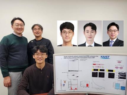
< (From left) Professor Seyun Kim, Professor Gwangrog Lee, Dr. Hyoungjoon Ahn, Dr. Jeongmin Yu, Professor Won-Ki Cho, and (below) PhD candidate Kwangmin Ryu of the Department of Biological Sciences>
A research team at KAIST has identified the core gene expression networks regulated by key proteins that fundamentally drive phenomena such as cancer development, metastasis, tissue differentiation from stem cells, and neural activation processes. This discovery lays the foundation for developing innovative therapeutic technologies.
On the 22nd of January, KAIST (represented by President Kwang Hyung Lee) announced that the joint research team led by Professors Seyun Kim, Gwangrog Lee, and Won-Ki Cho from the Department of Biological Sciences had uncovered essential mechanisms controlling gene expression in animal cells.
Inositol phosphate metabolites produced by inositol metabolism enzymes serve as vital secondary messengers in eukaryotic cell signaling systems and are broadly implicated in cancer, obesity, diabetes, and neurological disorders.
The research team demonstrated that the inositol polyphosphate multikinase (IPMK) enzyme, a key player in the inositol metabolism system, acts as a critical transcriptional activator within the core gene expression networks of animal cells. Notably, although IPMK was previously reported to play an important role in the transcription process governed by serum response factor (SRF), a representative transcription factor in animal cells, the precise mechanism of its action was unclear.
SRF is a transcription factor directly controlling the expression of at least 200–300 genes, regulating cell growth, proliferation, apoptosis, and motility, and is indispensable for organ development, such as in the heart.
The team discovered that IPMK binds directly to SRF, altering the three-dimensional structure of the SRF protein. This interaction facilitates the transcriptional activity of various genes through the SRF activated by IPMK, demonstrating that IPMK acts as a critical regulatory switch to enhance SRF's protein activity.
< Figure 1. The serum response factor (SRF) protein, a key transcription factor in animal cells, directly binds to inositol polyphosphate multikinase (IPMK) enzyme and undergoes structural change to acquire DNA binding ability, and precisely regulates growth and differentiation of animal cells through transcriptional activation. >
The team further verified that disruptions in the direct interaction between IPMK and SRF lead to the reduced functionality and activity of SRF, causing severe impairments in gene expression.
By highlighting the significance of the intrinsically disordered region (IDR) in SRF, the researchers underscored the biological importance of intrinsically disordered proteins (IDPs). Unlike most proteins that adopt distinct structures through folding, IDPs, including those with IDRs, do not exhibit specific structures but play crucial biological roles, attracting significant attention in the scientific community.
Professor Seyun Kim commented, "This study provides a vital mechanism proving that IPMK, a key enzyme in the inositol metabolism system, is a major transcriptional activator in the core gene expression network of animal cells. By understanding fundamental processes such as cancer development and metastasis, tissue differentiation from stem cells, and neural activation through SRF, we hope this discovery will lead to the broad application of innovative therapeutic technologies."
The findings were published on January 7th in the international journal Nucleic Acids Research (IF=16.7, top 1.8% in Biochemistry and Molecular Biology), under the title “Single-molecule analysis reveals that IPMK enhances the DNA-binding activity of the transcription factor SRF" (DOI: 10.1093/nar/gkae1281).
This research was supported by the National Research Foundation of Korea's Mid-career Research Program, Leading Research Center Program, and Global Research Laboratory Program, as well as by the Suh Kyungbae Science Foundation and the Samsung Future Technology Development Program.
2025.01.24 View 7827
KAIST Uncovers the Principles of Gene Expression Regulation in Cancer and Cellular Functions
< (From left) Professor Seyun Kim, Professor Gwangrog Lee, Dr. Hyoungjoon Ahn, Dr. Jeongmin Yu, Professor Won-Ki Cho, and (below) PhD candidate Kwangmin Ryu of the Department of Biological Sciences>
A research team at KAIST has identified the core gene expression networks regulated by key proteins that fundamentally drive phenomena such as cancer development, metastasis, tissue differentiation from stem cells, and neural activation processes. This discovery lays the foundation for developing innovative therapeutic technologies.
On the 22nd of January, KAIST (represented by President Kwang Hyung Lee) announced that the joint research team led by Professors Seyun Kim, Gwangrog Lee, and Won-Ki Cho from the Department of Biological Sciences had uncovered essential mechanisms controlling gene expression in animal cells.
Inositol phosphate metabolites produced by inositol metabolism enzymes serve as vital secondary messengers in eukaryotic cell signaling systems and are broadly implicated in cancer, obesity, diabetes, and neurological disorders.
The research team demonstrated that the inositol polyphosphate multikinase (IPMK) enzyme, a key player in the inositol metabolism system, acts as a critical transcriptional activator within the core gene expression networks of animal cells. Notably, although IPMK was previously reported to play an important role in the transcription process governed by serum response factor (SRF), a representative transcription factor in animal cells, the precise mechanism of its action was unclear.
SRF is a transcription factor directly controlling the expression of at least 200–300 genes, regulating cell growth, proliferation, apoptosis, and motility, and is indispensable for organ development, such as in the heart.
The team discovered that IPMK binds directly to SRF, altering the three-dimensional structure of the SRF protein. This interaction facilitates the transcriptional activity of various genes through the SRF activated by IPMK, demonstrating that IPMK acts as a critical regulatory switch to enhance SRF's protein activity.
< Figure 1. The serum response factor (SRF) protein, a key transcription factor in animal cells, directly binds to inositol polyphosphate multikinase (IPMK) enzyme and undergoes structural change to acquire DNA binding ability, and precisely regulates growth and differentiation of animal cells through transcriptional activation. >
The team further verified that disruptions in the direct interaction between IPMK and SRF lead to the reduced functionality and activity of SRF, causing severe impairments in gene expression.
By highlighting the significance of the intrinsically disordered region (IDR) in SRF, the researchers underscored the biological importance of intrinsically disordered proteins (IDPs). Unlike most proteins that adopt distinct structures through folding, IDPs, including those with IDRs, do not exhibit specific structures but play crucial biological roles, attracting significant attention in the scientific community.
Professor Seyun Kim commented, "This study provides a vital mechanism proving that IPMK, a key enzyme in the inositol metabolism system, is a major transcriptional activator in the core gene expression network of animal cells. By understanding fundamental processes such as cancer development and metastasis, tissue differentiation from stem cells, and neural activation through SRF, we hope this discovery will lead to the broad application of innovative therapeutic technologies."
The findings were published on January 7th in the international journal Nucleic Acids Research (IF=16.7, top 1.8% in Biochemistry and Molecular Biology), under the title “Single-molecule analysis reveals that IPMK enhances the DNA-binding activity of the transcription factor SRF" (DOI: 10.1093/nar/gkae1281).
This research was supported by the National Research Foundation of Korea's Mid-career Research Program, Leading Research Center Program, and Global Research Laboratory Program, as well as by the Suh Kyungbae Science Foundation and the Samsung Future Technology Development Program.
2025.01.24 View 7827 -
 KAIST Alumni Association to Honor Alumni of the Year Award Winners
Photo 1. Photo of the KAIST Alumni of the Year Award Recipients
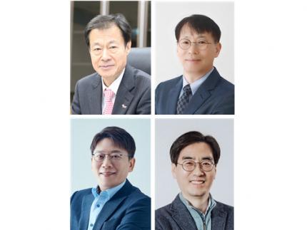
(From left) UST President Lee-whan Kim, CEO Han Chung of iThree Systems Co., Ltd., CEO Dong Myung Kim of LG Energy Solution Co., Ltd., and Professor Hyun Myung of the School of Electrical Engineering at KAIST
KAIST (President Kwang Hyung Lee) announced on Monday, the 13th of January that the Alumni Association (President Yun-Tae Lee) has selected its Alumni of the Year.
This year’s honorees are: ▴ President Lee-whan Kim of the Korea National University of Science and Technology (UST), ▴ CEO Han Chung of i3 Systems, ▴ CEO Dong Myung Kim of LG Energy Solution, and ▴ Professor Hyun Myung of the School of Electrical Engineering at KAIST.
The honorees were selected based on their achievements over the past year, and the award ceremony will be held at the 2025 KAIST Alumni Association New Year’s Gathering to be held at the L Tower in Seoul at 5 PM on Friday the 17th.
The KAIST Alumni of the Year Award is an award presented by the Alumni Association to alumni who have contributed to the development of the country and the society or have brought honor to their alma mater through outstanding academic achievements and community service. Since its establishment in 1992, 126 recipients have been awarded.
Lee-whan Kim (Master's graduate of Mechanical Engineering, 82), the President of the Korea National University of Science and Technology (UST), established a leading foundation for national science and technology policy and strategy, and played a leading role in innovating national science and technology capabilities through the advancement of the national research and development system and the advancement of science and technology personnel training. In particular, he played a pivotal role in the establishment of UST and the Korea Science Academy (KSA), and greatly contributed to establishing a foundation for the training and utilization of science and technology personnel.
Han Chung (Master's graduate of Electrical Engineering, 91, with Ph.D. degree in 96), the CEO of i3 Systems, is a first-generation researcher in the field of domestic infrared detectors. He developed military detectors for over 30 years and founded i3 Systems, a specialized infrared detector company, in 1998. Currently, he supplies more than 80% of the infrared detectors used by the Korean military, and has also achieved export results to over 20 countries.
Dong Myung Kim (Master's graduate of Materials Science and Engineering, 94, with Ph.D. degree in 98) the CEO of LG Energy Solution Co., Ltd. has led innovation in the battery field with his ceaseless exploration and challenging spirit, and is known as an authority in the secondary battery industry. He played a leading role in establishing K-Battery as a global leader, strengthened the country's future industrial competitiveness, and greatly contributed to the development of science and technology.
Hyun Myung (Bachelor's graduate of Electrical Engineering, 92, with Master's degree in 94, and Ph.D. degree in 98) a Professor of Electrical Engineering, KAIST, won first place in the world at the Quadruped Robot Challenge (QRC) hosted by the IEEE’s International Conference on Robotics and Automation (ICRA) 2023 with the 'DreamWaQ' system, an AI walking technology based on deep reinforcement learning that utilizes non-video sensory technologies. He contributed to enhancing the competitiveness of the domestic robot industry by developing his own fully autonomous walking technology that recognizes the environment around the robot and finds the optimal path.
Yun-Tae Lee, the 27th president of the KAIST Alumni Association, said, “KAIST alumni have been the driving force behind the growth of industries in all walks of life by continuously conducting research and development in the field of advanced science and technology for a long time,” and added, “I am very proud of the KAIST alumni award recipients who are leading science and technology on the world stage beyond Korea, and I sincerely thank them for their efforts and achievements.”
2025.01.15 View 3547
KAIST Alumni Association to Honor Alumni of the Year Award Winners
Photo 1. Photo of the KAIST Alumni of the Year Award Recipients
(From left) UST President Lee-whan Kim, CEO Han Chung of iThree Systems Co., Ltd., CEO Dong Myung Kim of LG Energy Solution Co., Ltd., and Professor Hyun Myung of the School of Electrical Engineering at KAIST
KAIST (President Kwang Hyung Lee) announced on Monday, the 13th of January that the Alumni Association (President Yun-Tae Lee) has selected its Alumni of the Year.
This year’s honorees are: ▴ President Lee-whan Kim of the Korea National University of Science and Technology (UST), ▴ CEO Han Chung of i3 Systems, ▴ CEO Dong Myung Kim of LG Energy Solution, and ▴ Professor Hyun Myung of the School of Electrical Engineering at KAIST.
The honorees were selected based on their achievements over the past year, and the award ceremony will be held at the 2025 KAIST Alumni Association New Year’s Gathering to be held at the L Tower in Seoul at 5 PM on Friday the 17th.
The KAIST Alumni of the Year Award is an award presented by the Alumni Association to alumni who have contributed to the development of the country and the society or have brought honor to their alma mater through outstanding academic achievements and community service. Since its establishment in 1992, 126 recipients have been awarded.
Lee-whan Kim (Master's graduate of Mechanical Engineering, 82), the President of the Korea National University of Science and Technology (UST), established a leading foundation for national science and technology policy and strategy, and played a leading role in innovating national science and technology capabilities through the advancement of the national research and development system and the advancement of science and technology personnel training. In particular, he played a pivotal role in the establishment of UST and the Korea Science Academy (KSA), and greatly contributed to establishing a foundation for the training and utilization of science and technology personnel.
Han Chung (Master's graduate of Electrical Engineering, 91, with Ph.D. degree in 96), the CEO of i3 Systems, is a first-generation researcher in the field of domestic infrared detectors. He developed military detectors for over 30 years and founded i3 Systems, a specialized infrared detector company, in 1998. Currently, he supplies more than 80% of the infrared detectors used by the Korean military, and has also achieved export results to over 20 countries.
Dong Myung Kim (Master's graduate of Materials Science and Engineering, 94, with Ph.D. degree in 98) the CEO of LG Energy Solution Co., Ltd. has led innovation in the battery field with his ceaseless exploration and challenging spirit, and is known as an authority in the secondary battery industry. He played a leading role in establishing K-Battery as a global leader, strengthened the country's future industrial competitiveness, and greatly contributed to the development of science and technology.
Hyun Myung (Bachelor's graduate of Electrical Engineering, 92, with Master's degree in 94, and Ph.D. degree in 98) a Professor of Electrical Engineering, KAIST, won first place in the world at the Quadruped Robot Challenge (QRC) hosted by the IEEE’s International Conference on Robotics and Automation (ICRA) 2023 with the 'DreamWaQ' system, an AI walking technology based on deep reinforcement learning that utilizes non-video sensory technologies. He contributed to enhancing the competitiveness of the domestic robot industry by developing his own fully autonomous walking technology that recognizes the environment around the robot and finds the optimal path.
Yun-Tae Lee, the 27th president of the KAIST Alumni Association, said, “KAIST alumni have been the driving force behind the growth of industries in all walks of life by continuously conducting research and development in the field of advanced science and technology for a long time,” and added, “I am very proud of the KAIST alumni award recipients who are leading science and technology on the world stage beyond Korea, and I sincerely thank them for their efforts and achievements.”
2025.01.15 View 3547 -
 “Cross-Generation Collaborative Labs” for Semiconductor, Chemistry, and Computer Science Opened
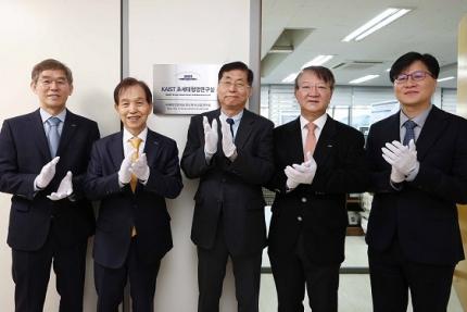
< Photo of Professor Hoi-Jun Yoo (center) of the School of Electrical Engineering at the signboard unveiling ceremony >
KAIST held a ceremony to mark the opening of three additional ‘Cross-Generation Collaborative Labs’ on the morning of January 7th, 2025.
The “Next-Generation AI Semiconductor System Lab” by Professor Hoi-Jun Yoo of the School of Electrical Engineering, the “Molecular Spectroscopy and Chemical Dynamics Lab” by Professor Sang Kyu Kim of the Department of Chemistry, and the “Advanced Data Computing Lab” by Professor Sue Bok Moon of the School of Computer Science are the three new labs given the honored titled of the “Cross-Generation Collaborative Lab”.
The Cross-Generation Collaborative Lab is KAIST’s unique system that was set up to facilitate the collaboration between retiring professors and junior professors to continue the achievements and know-how the elders have accumulated over their academic career. Since its introduction in 2018, nine labs have been named to be the Cross-Generation Labs, and this year’s new addition brings the total up to twelve.
The ‘Next-Generation AI Semiconductor System Lab’ led by Professor Hoi-Jun Yoo will be operated by Professor Joo-Young Kim of the same school.
Professor Hoi-Jun Yoo is a world-renowned scholar with outstanding research achievements in the field of on-device AI semiconductor design. Professor Joo-Young Kim is an up-and-coming researcher studying large language models and design of AI semiconductors for server computers, and is currently researching technologies to design PIM (Processing-in-Memory), a core technology in the field of AI semiconductors.
Their research goal is to systematically collaborate and transfer next-generation AI semiconductor design technology, including brain-mimicking AI algorithms such as deep neural networks and generative AI, to integrate core technologies, and to maximize the usability of R&D outputs, thereby further solidifying the position of Korean AI semiconductor companies in the global market.
Professor Hoi-Jun Yoo said, “I believe that, we will be able to present a development direction of for the next-generation AI semiconductors industries at home and abroad through collaborative research and play a key role in transferring and expanding global leadership.”
< Professor Sang Kyu Kim of the Department of Chemistry (middle), at the signboard unveiling ceremony for his laboratory >
The “Molecular Spectroscopy and Chemical Dynamics Laboratory”, where Professor Sang Kyu Kim of the Department of Chemistry is in charge, will be operated by Professor Tae Kyu Kim of the same department, and another professor in the field of spectroscopy and dynamics will join in the future.
Professor Sang Kyu Kim has secured technologies for developing unique experimental equipment based on ultrashort lasers and supersonic molecular beams, and is a world leader who has been creatively pioneering new fields of experimental physical chemistry.
The research goal is to describe chemical reactions and verify from a quantum mechanical perspective and introduce new theories and technologies to pursue a complete understanding of the principles of chemical reactions. In addition, the accompanying basic scientific knowledge will be applied to the design of new materials.
Professor Sang Kyu Kim said, “I am very happy to be able to pass on the research infrastructure to the next generation through this system, and I will continue to nurture it to grow into a world-class research lab through trans-generational collaborative research.”
< Photo of Professor Sue Bok Moon (center) at the signboard unveiling ceremony by the School of Computing >
Lastly, the “Advanced Data Computing Lab” led by Professor Sue Bok Moon is joined by Professor Mee Young Cha of the same school and Professor Wonjae Lee of the Graduate School of Culture Technology.
Professor Sue Bok Moon showed the infinite possibilities of large-scale data-based social network research through Cyworld, YouTube, and Twitter, and had a great influence on related fields beyond the field of computer science.
Professor Mee Young Cha is a data scientist who analyzes difficult social issues such as misinformation, poverty, and disaster detection using big data-based AI. She is the first Korean to be recognized for her achievements as the director of the Max Planck Institute in Germany, a world-class basic science research institute. Therefore, there is high expectation for synergy effects from overseas collaborative research and technology transfer and sharing among the participating professors of the collaborative research lab. Professor Wonjae Lee is researching dynamic interaction analysis between science and technology using structural topic models.
They plan to conduct research aimed at improving the analysis and understanding of negative influences occurring online, and in particular, developing a hateful precursor detection model using emotions and morality to preemptively block hateful expressions.
Professor Sue Bok Moon said, “Through this collaborative research lab, we will play a key role in conducting in-depth collaborative research on unexpected negative influences in the AI era so that we can have a high level of competitiveness worldwide.”
The ceremonies for the unveiling of the new Cross-Generation Collaborative Lab signboard were held in front of each lab from 10:00 AM on the 7th, in the attendance of President Kwang Hyung Lee, Senior Vice President for Research Sang Yup Lee, and other key officials of KAIST and the new staff members to join the laboratories.
2025.01.07 View 3214
“Cross-Generation Collaborative Labs” for Semiconductor, Chemistry, and Computer Science Opened
< Photo of Professor Hoi-Jun Yoo (center) of the School of Electrical Engineering at the signboard unveiling ceremony >
KAIST held a ceremony to mark the opening of three additional ‘Cross-Generation Collaborative Labs’ on the morning of January 7th, 2025.
The “Next-Generation AI Semiconductor System Lab” by Professor Hoi-Jun Yoo of the School of Electrical Engineering, the “Molecular Spectroscopy and Chemical Dynamics Lab” by Professor Sang Kyu Kim of the Department of Chemistry, and the “Advanced Data Computing Lab” by Professor Sue Bok Moon of the School of Computer Science are the three new labs given the honored titled of the “Cross-Generation Collaborative Lab”.
The Cross-Generation Collaborative Lab is KAIST’s unique system that was set up to facilitate the collaboration between retiring professors and junior professors to continue the achievements and know-how the elders have accumulated over their academic career. Since its introduction in 2018, nine labs have been named to be the Cross-Generation Labs, and this year’s new addition brings the total up to twelve.
The ‘Next-Generation AI Semiconductor System Lab’ led by Professor Hoi-Jun Yoo will be operated by Professor Joo-Young Kim of the same school.
Professor Hoi-Jun Yoo is a world-renowned scholar with outstanding research achievements in the field of on-device AI semiconductor design. Professor Joo-Young Kim is an up-and-coming researcher studying large language models and design of AI semiconductors for server computers, and is currently researching technologies to design PIM (Processing-in-Memory), a core technology in the field of AI semiconductors.
Their research goal is to systematically collaborate and transfer next-generation AI semiconductor design technology, including brain-mimicking AI algorithms such as deep neural networks and generative AI, to integrate core technologies, and to maximize the usability of R&D outputs, thereby further solidifying the position of Korean AI semiconductor companies in the global market.
Professor Hoi-Jun Yoo said, “I believe that, we will be able to present a development direction of for the next-generation AI semiconductors industries at home and abroad through collaborative research and play a key role in transferring and expanding global leadership.”
< Professor Sang Kyu Kim of the Department of Chemistry (middle), at the signboard unveiling ceremony for his laboratory >
The “Molecular Spectroscopy and Chemical Dynamics Laboratory”, where Professor Sang Kyu Kim of the Department of Chemistry is in charge, will be operated by Professor Tae Kyu Kim of the same department, and another professor in the field of spectroscopy and dynamics will join in the future.
Professor Sang Kyu Kim has secured technologies for developing unique experimental equipment based on ultrashort lasers and supersonic molecular beams, and is a world leader who has been creatively pioneering new fields of experimental physical chemistry.
The research goal is to describe chemical reactions and verify from a quantum mechanical perspective and introduce new theories and technologies to pursue a complete understanding of the principles of chemical reactions. In addition, the accompanying basic scientific knowledge will be applied to the design of new materials.
Professor Sang Kyu Kim said, “I am very happy to be able to pass on the research infrastructure to the next generation through this system, and I will continue to nurture it to grow into a world-class research lab through trans-generational collaborative research.”
< Photo of Professor Sue Bok Moon (center) at the signboard unveiling ceremony by the School of Computing >
Lastly, the “Advanced Data Computing Lab” led by Professor Sue Bok Moon is joined by Professor Mee Young Cha of the same school and Professor Wonjae Lee of the Graduate School of Culture Technology.
Professor Sue Bok Moon showed the infinite possibilities of large-scale data-based social network research through Cyworld, YouTube, and Twitter, and had a great influence on related fields beyond the field of computer science.
Professor Mee Young Cha is a data scientist who analyzes difficult social issues such as misinformation, poverty, and disaster detection using big data-based AI. She is the first Korean to be recognized for her achievements as the director of the Max Planck Institute in Germany, a world-class basic science research institute. Therefore, there is high expectation for synergy effects from overseas collaborative research and technology transfer and sharing among the participating professors of the collaborative research lab. Professor Wonjae Lee is researching dynamic interaction analysis between science and technology using structural topic models.
They plan to conduct research aimed at improving the analysis and understanding of negative influences occurring online, and in particular, developing a hateful precursor detection model using emotions and morality to preemptively block hateful expressions.
Professor Sue Bok Moon said, “Through this collaborative research lab, we will play a key role in conducting in-depth collaborative research on unexpected negative influences in the AI era so that we can have a high level of competitiveness worldwide.”
The ceremonies for the unveiling of the new Cross-Generation Collaborative Lab signboard were held in front of each lab from 10:00 AM on the 7th, in the attendance of President Kwang Hyung Lee, Senior Vice President for Research Sang Yup Lee, and other key officials of KAIST and the new staff members to join the laboratories.
2025.01.07 View 3214 -
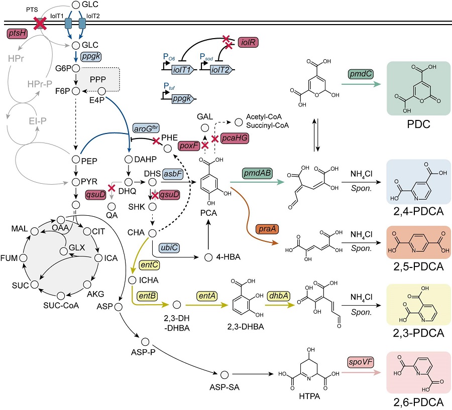 KAIST Researchers Suggest an Extraordinary Alternative to Petroleum-based PET - Bacteria!
< (From left) Dr. Cindy Pricilia, Ph.D. Candidate Cheon Woo Moon, Distinguished Professor Sang Yup Lee >
Currently, the world is suffering from environmental problems caused by plastic waste. The KAIST research team has succeeded in producing a microbial-based plastic that is biodegradable and can replace existing PET bottles, making it a hot topic.
Our university announced on the 7th of November that the research team of Distinguished Professor Sang Yup Lee of the Department of Chemical and Biomolecular Engineering has succeeded in developing a microbial strain that efficiently produces pseudoaromatic polyester monomer to replace polyethylene terephthalate (PET) using systems metabolic engineering.
Pseudoaromatic dicarboxylic acids have better physical properties and higher biodegradability than aromatic polyester (PET) when synthesized as polymers, and are attracting attention as an eco-friendly monomer* that can be synthesized into polymers. The production of pseudoaromatic dicarboxylic acids through chemical methods has the problems of low yield and selectivity, complex reaction conditions, and the generation of hazardous waste.
*Monomer: A material for making polymers, which is used to synthesize polymers by polymerizing monomers together
< Figure. Overview of pseudoaromatic dicarboxylic acid production using metabolically engineered C. glutamicum. >
To solve this problem, Professor Sang Yup Lee's research team used metabolic engineering to develop a microbial strain that efficiently produces five types of pseudoaromatic dicarboxylic acids, including 2-pyrone-4,6-dicarboxylic acid and four types of pyridine dicarboxylic acids (2,3-, 2,4-, 2,5-, 2,6-pyridine dicarboxylic acids), in Corynebacterium, a bacterium mainly used for amino acid production.
The research team used metabolic engineering techniques to build a platform microbial strain that enhances the metabolic flow of protocatechuic acid, which is used as a precursor for several pseudoaromatic dicarboxylic acids, and prevents the loss of precursors.
Based on this, the genetic manipulation target was discovered through transcriptome analysis, producing 76.17 g/L of 2-pyrone-4,6-dicarboxylic acid, and by newly discovering and constructing three types of pyridine dicarboxylic acid production metabolic pathways, successfully producing 2.79 g/L of 2,3-pyridine dicarboxylic acid, 0.49 g/L of 2,4-pyridine dicarboxylic acid, and 1.42 g/L of 2,5-pyridine dicarboxylic acid.
In addition, the research team confirmed the production of 15.01 g/L through the construction and reinforcement of the 2,6-pyridine dicarboxylic acid biosynthesis pathway, successfully producing a total of five similar aromatic dicarboxylic acids with high efficiency.
In conclusion, the team succeeded in producing 2,4-, 2,5-, and 2,6-pyridine dicarboxylic acids at the world's highest concentration. In particular, 2,4-, 2,5-pyridine dicarboxylic acid achieved production on the scale of g/L, which was previously produced in extremely small amounts (mg/L).
Based on this study, it is expected that it will be applied to various polyester production industrial processes, and it is also expected that it will be actively utilized in research on the production of similar aromatic polyesters.
Professor Sang Yup Lee, the corresponding author, said, “The significance lies in the fact that we have developed an eco-friendly technology that efficiently produces similar aromatic polyester monomers based on microorganisms,” and “This study will help the microorganism-based bio-monomer industry replace the petrochemical-based chemical industry in the future.”
The results of this study were published in the international academic journal, the Proceedings of the National Academy of Sciences of United States of America (PNAS) on October 30th.
※ Paper title: Metabolic engineering of Corynebacterium glutamicum for the production of pyrone and pyridine dicarboxylic acids
※ Author information: Jae Sung Cho (co-first author), Zi Wei Luo (co-first author), Cheon Woo Moon (co-first author), Cindy Prabowo (co-author), Sang Yup Lee (corresponding author) - a total of 5 people
This study was conducted with the support of the Development of Next-generation Biorefinery Platform Technologies for Leading Bio-based Chemicals Industry Project and the Development of Platform Technologies of Microbial Cell Factories for the Next-generation Biorefineries Project (Project leader: Professor Sang Yup Lee) from the National Research Foundation supported by the Ministry of Science and Technology and ICT of Korea.
2024.11.08 View 6990
KAIST Researchers Suggest an Extraordinary Alternative to Petroleum-based PET - Bacteria!
< (From left) Dr. Cindy Pricilia, Ph.D. Candidate Cheon Woo Moon, Distinguished Professor Sang Yup Lee >
Currently, the world is suffering from environmental problems caused by plastic waste. The KAIST research team has succeeded in producing a microbial-based plastic that is biodegradable and can replace existing PET bottles, making it a hot topic.
Our university announced on the 7th of November that the research team of Distinguished Professor Sang Yup Lee of the Department of Chemical and Biomolecular Engineering has succeeded in developing a microbial strain that efficiently produces pseudoaromatic polyester monomer to replace polyethylene terephthalate (PET) using systems metabolic engineering.
Pseudoaromatic dicarboxylic acids have better physical properties and higher biodegradability than aromatic polyester (PET) when synthesized as polymers, and are attracting attention as an eco-friendly monomer* that can be synthesized into polymers. The production of pseudoaromatic dicarboxylic acids through chemical methods has the problems of low yield and selectivity, complex reaction conditions, and the generation of hazardous waste.
*Monomer: A material for making polymers, which is used to synthesize polymers by polymerizing monomers together
< Figure. Overview of pseudoaromatic dicarboxylic acid production using metabolically engineered C. glutamicum. >
To solve this problem, Professor Sang Yup Lee's research team used metabolic engineering to develop a microbial strain that efficiently produces five types of pseudoaromatic dicarboxylic acids, including 2-pyrone-4,6-dicarboxylic acid and four types of pyridine dicarboxylic acids (2,3-, 2,4-, 2,5-, 2,6-pyridine dicarboxylic acids), in Corynebacterium, a bacterium mainly used for amino acid production.
The research team used metabolic engineering techniques to build a platform microbial strain that enhances the metabolic flow of protocatechuic acid, which is used as a precursor for several pseudoaromatic dicarboxylic acids, and prevents the loss of precursors.
Based on this, the genetic manipulation target was discovered through transcriptome analysis, producing 76.17 g/L of 2-pyrone-4,6-dicarboxylic acid, and by newly discovering and constructing three types of pyridine dicarboxylic acid production metabolic pathways, successfully producing 2.79 g/L of 2,3-pyridine dicarboxylic acid, 0.49 g/L of 2,4-pyridine dicarboxylic acid, and 1.42 g/L of 2,5-pyridine dicarboxylic acid.
In addition, the research team confirmed the production of 15.01 g/L through the construction and reinforcement of the 2,6-pyridine dicarboxylic acid biosynthesis pathway, successfully producing a total of five similar aromatic dicarboxylic acids with high efficiency.
In conclusion, the team succeeded in producing 2,4-, 2,5-, and 2,6-pyridine dicarboxylic acids at the world's highest concentration. In particular, 2,4-, 2,5-pyridine dicarboxylic acid achieved production on the scale of g/L, which was previously produced in extremely small amounts (mg/L).
Based on this study, it is expected that it will be applied to various polyester production industrial processes, and it is also expected that it will be actively utilized in research on the production of similar aromatic polyesters.
Professor Sang Yup Lee, the corresponding author, said, “The significance lies in the fact that we have developed an eco-friendly technology that efficiently produces similar aromatic polyester monomers based on microorganisms,” and “This study will help the microorganism-based bio-monomer industry replace the petrochemical-based chemical industry in the future.”
The results of this study were published in the international academic journal, the Proceedings of the National Academy of Sciences of United States of America (PNAS) on October 30th.
※ Paper title: Metabolic engineering of Corynebacterium glutamicum for the production of pyrone and pyridine dicarboxylic acids
※ Author information: Jae Sung Cho (co-first author), Zi Wei Luo (co-first author), Cheon Woo Moon (co-first author), Cindy Prabowo (co-author), Sang Yup Lee (corresponding author) - a total of 5 people
This study was conducted with the support of the Development of Next-generation Biorefinery Platform Technologies for Leading Bio-based Chemicals Industry Project and the Development of Platform Technologies of Microbial Cell Factories for the Next-generation Biorefineries Project (Project leader: Professor Sang Yup Lee) from the National Research Foundation supported by the Ministry of Science and Technology and ICT of Korea.
2024.11.08 View 6990 -
 KAIST finds ways for Bacteria to produce PET-like materials
Among various eco-friendly polymers, polyhydroxyalkanoates (PHA) stand out for their excellent biodegradability and biocompatibility. They decompose naturally in soil and marine environments and are used in applications such as food packaging and medical products. However, natural PHA produced to date has faced challenges meeting various physical property requirements, such as durability and thermal stability, and has been limited in its commercial application due to low production concentrations. In light of this, KAIST researchers have recently developed a technology that could play a crucial role in solving the environmental pollution problem caused by plastics.
KAIST (represented by President Kwang-Hyung Lee) announced on August 26th that a research team led by Distinguished Professor Sang Yup Lee from the Department of Chemical and Biomolecular Engineering, including Dr. Youngjoon Lee and master's student Minju Kang, has successfully developed a microbial strain that efficiently produces aromatic polyester* using systems metabolic engineering.
※ Aromatic polyester: A polymer containing aromatic compounds (specific carbon ring structures like benzene) and ester bonds.
In this study, the research team used metabolic engineering to enhance the metabolic flux of the biosynthetic pathway for the aromatic monomer phenyllactate (PhLA) in E. coli. They manipulated the metabolic pathway to increase the polymer fraction accumulated within the cells and employed computer simulations to predict the structure of PHA synthase and improve the enzyme based on the structure-function relationship.
Through subsequent fermentation optimization, the team achieved the world’s highest concentration (12.3±0.1 g/L) for the efficient production of poly (PhLA) and successfully produced polyester through a 30L scale fed-batch fermentation, demonstrating the possibility of industrial-level production. The produced aromatic polyesters showed enhanced thermal properties, improved mechanical properties, and potential for use as drug delivery carriers.
< Figure 1. Development schematics of aromatic polyester producing microorganisms >
The research team also demonstrated that an exogenous phasin protein* plays a crucial role in increasing the intracellular polymer accumulation fraction, which is directly related to the economic feasibility and efficiency of non-natural PHA production. They improved PHA synthase using a rational enzyme design approach, predicting the three-dimensional structure of the enzyme through homology modeling (a method of predicting the three-dimensional structure of a new protein based on the structure of similar proteins) followed by molecular docking simulations (simulations that predict how well a monomer can bind to an enzyme) and molecular dynamics simulations (simulations that predict how molecules move and interact over time) to upgrade the enzyme into a mutant enzyme with enhanced monomer polymerization efficiency.
※ Exogenous phasin protein: Phasin is a protein related to PHA production, interacting with the cytoplasmic environment on the surface of granules of PHA, and playing a role in polymer accumulation and controlling the number and size of granules. In this study, genes encoding phasin proteins derived from various natural PHA-producing microorganisms were selected and introduced.
Dr. Youngjoon Lee, co-first author of the paper, explained, "The significance of this study lies in the fact that we have achieved the world's highest concentration of microbial-based aromatic polyester production using eco-friendly materials and methods. This technology is expected to play a crucial role in addressing the environmental pollution caused by plastics." Distinguished Professor Sang Yup Lee added, "This study, which presents various strategies for the high-efficiency production of useful polymers via systems metabolic engineering, is expected to make a significant contribution to solving climate change issues, particularly the recent plastic problem."
< Figure 2. Detailed development strategy for aromatic polyester producing microorganisms >
The research findings were published on August 21st in Trends in Biotechnology, published by Cell, an international academic journal.
※ Paper Title: “Microbial production of an aromatic homopolyester”
※ Author Information: Youngjoon Lee (KAIST, co-first author), Minju Kang (KAIST, co-first author), Woo Dae Jang (KAIST, second author), So Young Choi (KAIST, third author), Jung Eun Yang (KAIST, fourth author), Sang Yup Lee (KAIST, corresponding author), totaling six authors.
This research was supported by the "Development of Next-Generation Biorefinery Platform Technologies for Leading the Bio-based Chemicals Industry" project led by Distinguished Professor Sang Yup Lee at KAIST, under the eco-friendly chemical technology development project aimed at substituting petroleum, funded by the Ministry of Science and ICT. It was also supported by the "Development of Platform Technology for the Production of Novel Aromatic Bioplastic Using Microbial Cell Factories" project (Project Leader: Si Jae Park, Ewha Woman’s University).
2024.08.28 View 5313
KAIST finds ways for Bacteria to produce PET-like materials
Among various eco-friendly polymers, polyhydroxyalkanoates (PHA) stand out for their excellent biodegradability and biocompatibility. They decompose naturally in soil and marine environments and are used in applications such as food packaging and medical products. However, natural PHA produced to date has faced challenges meeting various physical property requirements, such as durability and thermal stability, and has been limited in its commercial application due to low production concentrations. In light of this, KAIST researchers have recently developed a technology that could play a crucial role in solving the environmental pollution problem caused by plastics.
KAIST (represented by President Kwang-Hyung Lee) announced on August 26th that a research team led by Distinguished Professor Sang Yup Lee from the Department of Chemical and Biomolecular Engineering, including Dr. Youngjoon Lee and master's student Minju Kang, has successfully developed a microbial strain that efficiently produces aromatic polyester* using systems metabolic engineering.
※ Aromatic polyester: A polymer containing aromatic compounds (specific carbon ring structures like benzene) and ester bonds.
In this study, the research team used metabolic engineering to enhance the metabolic flux of the biosynthetic pathway for the aromatic monomer phenyllactate (PhLA) in E. coli. They manipulated the metabolic pathway to increase the polymer fraction accumulated within the cells and employed computer simulations to predict the structure of PHA synthase and improve the enzyme based on the structure-function relationship.
Through subsequent fermentation optimization, the team achieved the world’s highest concentration (12.3±0.1 g/L) for the efficient production of poly (PhLA) and successfully produced polyester through a 30L scale fed-batch fermentation, demonstrating the possibility of industrial-level production. The produced aromatic polyesters showed enhanced thermal properties, improved mechanical properties, and potential for use as drug delivery carriers.
< Figure 1. Development schematics of aromatic polyester producing microorganisms >
The research team also demonstrated that an exogenous phasin protein* plays a crucial role in increasing the intracellular polymer accumulation fraction, which is directly related to the economic feasibility and efficiency of non-natural PHA production. They improved PHA synthase using a rational enzyme design approach, predicting the three-dimensional structure of the enzyme through homology modeling (a method of predicting the three-dimensional structure of a new protein based on the structure of similar proteins) followed by molecular docking simulations (simulations that predict how well a monomer can bind to an enzyme) and molecular dynamics simulations (simulations that predict how molecules move and interact over time) to upgrade the enzyme into a mutant enzyme with enhanced monomer polymerization efficiency.
※ Exogenous phasin protein: Phasin is a protein related to PHA production, interacting with the cytoplasmic environment on the surface of granules of PHA, and playing a role in polymer accumulation and controlling the number and size of granules. In this study, genes encoding phasin proteins derived from various natural PHA-producing microorganisms were selected and introduced.
Dr. Youngjoon Lee, co-first author of the paper, explained, "The significance of this study lies in the fact that we have achieved the world's highest concentration of microbial-based aromatic polyester production using eco-friendly materials and methods. This technology is expected to play a crucial role in addressing the environmental pollution caused by plastics." Distinguished Professor Sang Yup Lee added, "This study, which presents various strategies for the high-efficiency production of useful polymers via systems metabolic engineering, is expected to make a significant contribution to solving climate change issues, particularly the recent plastic problem."
< Figure 2. Detailed development strategy for aromatic polyester producing microorganisms >
The research findings were published on August 21st in Trends in Biotechnology, published by Cell, an international academic journal.
※ Paper Title: “Microbial production of an aromatic homopolyester”
※ Author Information: Youngjoon Lee (KAIST, co-first author), Minju Kang (KAIST, co-first author), Woo Dae Jang (KAIST, second author), So Young Choi (KAIST, third author), Jung Eun Yang (KAIST, fourth author), Sang Yup Lee (KAIST, corresponding author), totaling six authors.
This research was supported by the "Development of Next-Generation Biorefinery Platform Technologies for Leading the Bio-based Chemicals Industry" project led by Distinguished Professor Sang Yup Lee at KAIST, under the eco-friendly chemical technology development project aimed at substituting petroleum, funded by the Ministry of Science and ICT. It was also supported by the "Development of Platform Technology for the Production of Novel Aromatic Bioplastic Using Microbial Cell Factories" project (Project Leader: Si Jae Park, Ewha Woman’s University).
2024.08.28 View 5313 -
 KAIST Research Team Creates the Scent of Jasmine from Microorganisms
The fragrance of jasmine and ylang-ylang, used widely in the manufacturing of cosmetics, foods, and beverages, can be produced by direct extraction from their respective flowers. In reality, this makes it difficult for production to meet demand, so companies use benzyl acetate, a major aromatic component of the two fragrances that is chemically synthesized from raw materials derived from petroleum.
On February 26, a KAIST research team led by Research Professor Kyeong Rok Choi from the BioProcess Engineering Research Center and Distinguished Professor Sang Yup Lee from the Department of Chemical and Biomolecular Engineering revealed the development of the first microbial process to effectively produce benzyl acetate, an industrially useful compound, from renewable carbon sources such as glucose. The results were published in their paper titled “A microbial process for the production of benzyl acetate”.
< Figure 1. Production of benzyl acetate through co-culture of upstream and downstream strains harboring the benzoic acid-dependent pathway. >
The team, led by Distinguished Professor Lee, aimed to produce benzyl acetate through an environmentally friendly and sustainable method, and developed an Escherichia coli strand to convert glucose into benzyl acetate through system metabolic engineering*.
*System metabolic engineering: a field of research founded by Distinguished Professor Lee to effectively develop microbial cell plants, a core component of the bio-industry that will replace the existing chemical industry, which is highly dependent on petroleum.
The research team developed a metabolic pathway that biosynthesizes benzyl acetate from benzoic acid derived from glucose, and successfully produced benzyl acetate by co-culturing** the strain.
**co-culture: simultaneously synthesizing two or more types of microorganisms in a mixture
However, it has been confirmed that the enzyme used to convert benzoic acid into benzyl acetate in this co-culturing technique acts non-specifically on an intermediate product during benzoic acid biosynthesis, producing a by-product called cinnamyl acetate. This process consumes the intermediate product needed for benzoic acid biosynthesis, thereby reducing the production efficiency of the target compound, benzyl acetate.
To overcome this problem, Distinguished Professor Lee and his team devised a delayed co-culture method, where they first produced benzoic acid in the earlier stages of fermentation by only culturing the top strain that produces benzoic acid from glucose, and later inoculated the bottom strain to convert the accumulated benzoic acid in the culture medium into benzyl acetate.
By applying this co-culture technique, the team suppressed the formation of by-products without further strain improvement or applying additional enzymes, and multiplied the concentration of the target compound by 10 times, producing 2.2 g/L of benzyl acetate. In addition, the team confirmed its potential for the commercial production of benzyl acetate through a technical economic analysis on this microbial process.
< Figure 2. Delayed co-culture of the Bn1 and Bn-BnAc3 strains for improved production of benzyl acetate through the benzoic acid-independent pathway.>
Research Professor Keyong Rok Choi, who was the first author of this paper, said, “This work is significant in that we have developed an effective microbial process to produce the industrially useful compound benzyl acetate, and also in that we have suggested a new approach to overcome the target chemical efficiency diminution and by-product formation issues caused commonly through non-specific enzyme activities during metabolic engineering.”
Distinguished Professor Lee said, “If we can increase the variety and number of microbial processes that produce useful chemicals through sustainable methods and at the same time develop effective strategies to solve chronic and inevitable problems that arise during microbial strain development, we will be able to accelerate the transition from the petrochemical industry into the eco-friendly and sustainable bio-industry.
This work was published online in Nature Chemical Engineering, issued by Nature.
This research was supported by the ‘Implementation of Intelligent Cell Factory Technology (PI: Distinguished Professor Sang Yup Lee) Project by the Ministry of Science and ICT, and the ‘Development of Protein Production Technology from Inorganic Substances through Microbiological Metabolic System Control’ (PI: Research Professor Kyeong Rok Choi) by the Agricultural Microbiological Project Group at the Rural Development Administration.
2024.03.05 View 6080
KAIST Research Team Creates the Scent of Jasmine from Microorganisms
The fragrance of jasmine and ylang-ylang, used widely in the manufacturing of cosmetics, foods, and beverages, can be produced by direct extraction from their respective flowers. In reality, this makes it difficult for production to meet demand, so companies use benzyl acetate, a major aromatic component of the two fragrances that is chemically synthesized from raw materials derived from petroleum.
On February 26, a KAIST research team led by Research Professor Kyeong Rok Choi from the BioProcess Engineering Research Center and Distinguished Professor Sang Yup Lee from the Department of Chemical and Biomolecular Engineering revealed the development of the first microbial process to effectively produce benzyl acetate, an industrially useful compound, from renewable carbon sources such as glucose. The results were published in their paper titled “A microbial process for the production of benzyl acetate”.
< Figure 1. Production of benzyl acetate through co-culture of upstream and downstream strains harboring the benzoic acid-dependent pathway. >
The team, led by Distinguished Professor Lee, aimed to produce benzyl acetate through an environmentally friendly and sustainable method, and developed an Escherichia coli strand to convert glucose into benzyl acetate through system metabolic engineering*.
*System metabolic engineering: a field of research founded by Distinguished Professor Lee to effectively develop microbial cell plants, a core component of the bio-industry that will replace the existing chemical industry, which is highly dependent on petroleum.
The research team developed a metabolic pathway that biosynthesizes benzyl acetate from benzoic acid derived from glucose, and successfully produced benzyl acetate by co-culturing** the strain.
**co-culture: simultaneously synthesizing two or more types of microorganisms in a mixture
However, it has been confirmed that the enzyme used to convert benzoic acid into benzyl acetate in this co-culturing technique acts non-specifically on an intermediate product during benzoic acid biosynthesis, producing a by-product called cinnamyl acetate. This process consumes the intermediate product needed for benzoic acid biosynthesis, thereby reducing the production efficiency of the target compound, benzyl acetate.
To overcome this problem, Distinguished Professor Lee and his team devised a delayed co-culture method, where they first produced benzoic acid in the earlier stages of fermentation by only culturing the top strain that produces benzoic acid from glucose, and later inoculated the bottom strain to convert the accumulated benzoic acid in the culture medium into benzyl acetate.
By applying this co-culture technique, the team suppressed the formation of by-products without further strain improvement or applying additional enzymes, and multiplied the concentration of the target compound by 10 times, producing 2.2 g/L of benzyl acetate. In addition, the team confirmed its potential for the commercial production of benzyl acetate through a technical economic analysis on this microbial process.
< Figure 2. Delayed co-culture of the Bn1 and Bn-BnAc3 strains for improved production of benzyl acetate through the benzoic acid-independent pathway.>
Research Professor Keyong Rok Choi, who was the first author of this paper, said, “This work is significant in that we have developed an effective microbial process to produce the industrially useful compound benzyl acetate, and also in that we have suggested a new approach to overcome the target chemical efficiency diminution and by-product formation issues caused commonly through non-specific enzyme activities during metabolic engineering.”
Distinguished Professor Lee said, “If we can increase the variety and number of microbial processes that produce useful chemicals through sustainable methods and at the same time develop effective strategies to solve chronic and inevitable problems that arise during microbial strain development, we will be able to accelerate the transition from the petrochemical industry into the eco-friendly and sustainable bio-industry.
This work was published online in Nature Chemical Engineering, issued by Nature.
This research was supported by the ‘Implementation of Intelligent Cell Factory Technology (PI: Distinguished Professor Sang Yup Lee) Project by the Ministry of Science and ICT, and the ‘Development of Protein Production Technology from Inorganic Substances through Microbiological Metabolic System Control’ (PI: Research Professor Kyeong Rok Choi) by the Agricultural Microbiological Project Group at the Rural Development Administration.
2024.03.05 View 6080 -
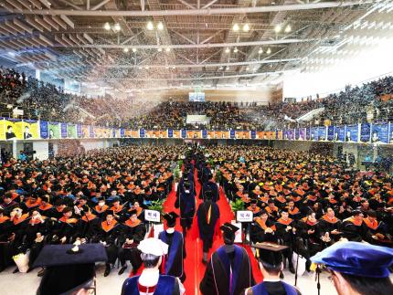 World-renowned Soprano Sumi Jo and Broadcom CEO Hock Tan awarded honorary doctorate from KAIST
< (From left) Sumi Jo, Distinguished Visiting Professor at the Graduate School of Culture and Technology, and Broadcom President and CEO Hock Tan >
KAIST (President Kwang-Hyung Lee) announced that it awarded honorary doctorates to world-renowned soprano Sumi Jo, a distinguished visiting professor at the Graduate School of Culture and Technology, and the President and Chief Executive Officer of Broadcom Inc., Hock Tan, at the graduation ceremony held on the 16th of February, 2024.
Professor Sumi Jo, who received an honorary doctorate in science and technology, was appointed as a visiting professor at KAIST Graduate School of Culture and Technology in 2021 and established the "Sumi Jo Performing Arts Research Center" and have been involved in research providing valuable feedback on projects to put on stage performances utilizing AI-orchestrated musical ensemble technology and research on virtual voices using vocal synthesis technology, as well as participating in the demonstration of the technological performance showcased at KAIST. Also, she held a special lecture and a talk concert for KAIST students, sharing her experience as a celebrated soprano on the world stage and having honest conversations with students.
KAIST said, “The doctorate is being awarded in recognition of her contributions that is broadening the spectrum of research in the field of science and technology to lead the digital era by suggesting a direction for future
science and technology to take led by culture. Also, her significant contribution to promoting necessary internationalization capabilities helps KAIST as it is growing into a world-class university through new academic challenges.”
< Professor Sumi Jo (left), who received an honorary doctorate in science and technology, and President Kwang-Hyung Lee >
Professor Sumi Jo, who debuted as Gilda in the opera in 1986, has performed with world-class conductors such as Herbert von Karajan, Georg Solti, Zubin Mehta, and James Levine. She has released over 40 full-length albums and continues to excel in all areas of vocal performances, including film scores, songs, and musicals.
Professor Sumi Jo said, “When I received a proposal from President Kwang-Hyung Lee of KAIST to convey what I experienced and felt on the world stage to students of science at KAIST under the topic of ‘Music and My Life,’ questions started to swirl inside of me.”
She continued, “Singing on stage is about ‘expressing,’ and it is a comprehensive artistic process that unfolding the artist’s inner self (expression) and showing it (presentation) in a way that the audience can best feel it through
methods such as sound, lighting, and directing. And I realized that, I was singing all my life in an environment where science and technology coexisted with culture and art.”
“When I worked with the students here at KAIST, I came to realize that when scientific and technologically talented people are set free to really enjoy their ideas and explore them on their own terms, their insight become sharper and their creativity become richer,” she said. She went on to add, “I am proud to be able to join the graduates at the ceremony and would like to express my gratitude for awarding me the honorary doctorate.”
< (From left) President Hock Tan, who received the honorary doctorate in engineering, Mrs. Lya Trung Tan, and President Kwang-Hyung Lee >
Hock Tan received an honorary doctorate in engineering. He is a highly successful businessman who demonstrated entrepreneurship based on a profound understanding of science and technology, which transformed Broadcom into a global enterprise in technology that provides semiconductor and software solutions.
Broadcom has achieved advancement and technological innovation in the semiconductor industry tailored to computer and telecommunication networks, and is evaluated as having played a major role in bringing about the digital transformation movement that is now encompassing the global communities.
Tan attributes the secret to his success to ‘the considerate decision made by the university to award him the scholarship which enabled him to pursue his degree’ and ‘the great team members working with him’..’ Also, he is well-known as a person who considers giving back to society his most important mission.
To support effective medical treatment and identification of the cause of autism, Tan has made large donations to MIT and Harvard University since 2017 several times, and during the COVID-19 pandemic, he reinforced his support to improve the treatment of workers at community medical institutions and non-profit organizations. He also founded the Broadcom Foundation, which supports science, technology, engineering, and mathematics (STEM) education programs for students in and outside the United States.
KAIST said, “We are awarding CEO Hock Tan the honorary doctorate in recognition of his contribution to KAIST’s emergence as a world-class university, as he emphasized the importance of convergence research and
internationalization of KAIST during his time serving as an overseas member of the KAIST President's Advisory Council from 2006 to 2013, while providing policy advices built on his experiences of innovations from various parts around the world.”
Tan emphasized, “KAIST has been vital to Korea’s advancement in the global economy. (KAIST) remains a source of technological innovation,” and that, “It is truly an honor to be recognized by an institution with such a distinguished record of excellence in science, engineering and research.”
President Kwang-Hyung Lee said, “Professor Sumi Jo’s exploration into the future of performing arts through science and technology helps to expand KAIST’s scope and enhance our creative capabilities, while the dedication and humane efforts Hock Tan demonstrates as he contributes to digital innovation through corporate management and engages in various social contribution activities serves as a superb example to all members of KAIST.”
He continued, “These two have lived out the values of challenge and innovation and became examples for many, and we are very pleased to welcome them as the newest members of the KAIST family. On behalf of all members of KAIST, I deliver our sincere congratulations.”
2024.02.17 View 10043
World-renowned Soprano Sumi Jo and Broadcom CEO Hock Tan awarded honorary doctorate from KAIST
< (From left) Sumi Jo, Distinguished Visiting Professor at the Graduate School of Culture and Technology, and Broadcom President and CEO Hock Tan >
KAIST (President Kwang-Hyung Lee) announced that it awarded honorary doctorates to world-renowned soprano Sumi Jo, a distinguished visiting professor at the Graduate School of Culture and Technology, and the President and Chief Executive Officer of Broadcom Inc., Hock Tan, at the graduation ceremony held on the 16th of February, 2024.
Professor Sumi Jo, who received an honorary doctorate in science and technology, was appointed as a visiting professor at KAIST Graduate School of Culture and Technology in 2021 and established the "Sumi Jo Performing Arts Research Center" and have been involved in research providing valuable feedback on projects to put on stage performances utilizing AI-orchestrated musical ensemble technology and research on virtual voices using vocal synthesis technology, as well as participating in the demonstration of the technological performance showcased at KAIST. Also, she held a special lecture and a talk concert for KAIST students, sharing her experience as a celebrated soprano on the world stage and having honest conversations with students.
KAIST said, “The doctorate is being awarded in recognition of her contributions that is broadening the spectrum of research in the field of science and technology to lead the digital era by suggesting a direction for future
science and technology to take led by culture. Also, her significant contribution to promoting necessary internationalization capabilities helps KAIST as it is growing into a world-class university through new academic challenges.”
< Professor Sumi Jo (left), who received an honorary doctorate in science and technology, and President Kwang-Hyung Lee >
Professor Sumi Jo, who debuted as Gilda in the opera in 1986, has performed with world-class conductors such as Herbert von Karajan, Georg Solti, Zubin Mehta, and James Levine. She has released over 40 full-length albums and continues to excel in all areas of vocal performances, including film scores, songs, and musicals.
Professor Sumi Jo said, “When I received a proposal from President Kwang-Hyung Lee of KAIST to convey what I experienced and felt on the world stage to students of science at KAIST under the topic of ‘Music and My Life,’ questions started to swirl inside of me.”
She continued, “Singing on stage is about ‘expressing,’ and it is a comprehensive artistic process that unfolding the artist’s inner self (expression) and showing it (presentation) in a way that the audience can best feel it through
methods such as sound, lighting, and directing. And I realized that, I was singing all my life in an environment where science and technology coexisted with culture and art.”
“When I worked with the students here at KAIST, I came to realize that when scientific and technologically talented people are set free to really enjoy their ideas and explore them on their own terms, their insight become sharper and their creativity become richer,” she said. She went on to add, “I am proud to be able to join the graduates at the ceremony and would like to express my gratitude for awarding me the honorary doctorate.”
< (From left) President Hock Tan, who received the honorary doctorate in engineering, Mrs. Lya Trung Tan, and President Kwang-Hyung Lee >
Hock Tan received an honorary doctorate in engineering. He is a highly successful businessman who demonstrated entrepreneurship based on a profound understanding of science and technology, which transformed Broadcom into a global enterprise in technology that provides semiconductor and software solutions.
Broadcom has achieved advancement and technological innovation in the semiconductor industry tailored to computer and telecommunication networks, and is evaluated as having played a major role in bringing about the digital transformation movement that is now encompassing the global communities.
Tan attributes the secret to his success to ‘the considerate decision made by the university to award him the scholarship which enabled him to pursue his degree’ and ‘the great team members working with him’..’ Also, he is well-known as a person who considers giving back to society his most important mission.
To support effective medical treatment and identification of the cause of autism, Tan has made large donations to MIT and Harvard University since 2017 several times, and during the COVID-19 pandemic, he reinforced his support to improve the treatment of workers at community medical institutions and non-profit organizations. He also founded the Broadcom Foundation, which supports science, technology, engineering, and mathematics (STEM) education programs for students in and outside the United States.
KAIST said, “We are awarding CEO Hock Tan the honorary doctorate in recognition of his contribution to KAIST’s emergence as a world-class university, as he emphasized the importance of convergence research and
internationalization of KAIST during his time serving as an overseas member of the KAIST President's Advisory Council from 2006 to 2013, while providing policy advices built on his experiences of innovations from various parts around the world.”
Tan emphasized, “KAIST has been vital to Korea’s advancement in the global economy. (KAIST) remains a source of technological innovation,” and that, “It is truly an honor to be recognized by an institution with such a distinguished record of excellence in science, engineering and research.”
President Kwang-Hyung Lee said, “Professor Sumi Jo’s exploration into the future of performing arts through science and technology helps to expand KAIST’s scope and enhance our creative capabilities, while the dedication and humane efforts Hock Tan demonstrates as he contributes to digital innovation through corporate management and engages in various social contribution activities serves as a superb example to all members of KAIST.”
He continued, “These two have lived out the values of challenge and innovation and became examples for many, and we are very pleased to welcome them as the newest members of the KAIST family. On behalf of all members of KAIST, I deliver our sincere congratulations.”
2024.02.17 View 10043